EP2009647A1 - Procede de fabrication de capteur a film mince, capteur a film mince et module de capteur a film mince - Google Patents
Procede de fabrication de capteur a film mince, capteur a film mince et module de capteur a film mince Download PDFInfo
- Publication number
- EP2009647A1 EP2009647A1 EP07740027A EP07740027A EP2009647A1 EP 2009647 A1 EP2009647 A1 EP 2009647A1 EP 07740027 A EP07740027 A EP 07740027A EP 07740027 A EP07740027 A EP 07740027A EP 2009647 A1 EP2009647 A1 EP 2009647A1
- Authority
- EP
- European Patent Office
- Prior art keywords
- thin
- film sensor
- film
- sensor
- electrical resistor
- Prior art date
- Legal status (The legal status is an assumption and is not a legal conclusion. Google has not performed a legal analysis and makes no representation as to the accuracy of the status listed.)
- Withdrawn
Links
Images


Classifications
-
- H—ELECTRICITY
- H01—ELECTRIC ELEMENTS
- H01C—RESISTORS
- H01C17/00—Apparatus or processes specially adapted for manufacturing resistors
- H01C17/06—Apparatus or processes specially adapted for manufacturing resistors adapted for coating resistive material on a base
- H01C17/075—Apparatus or processes specially adapted for manufacturing resistors adapted for coating resistive material on a base by thin-film techniques
- H01C17/12—Apparatus or processes specially adapted for manufacturing resistors adapted for coating resistive material on a base by thin-film techniques by sputtering
-
- G—PHYSICS
- G01—MEASURING; TESTING
- G01J—MEASUREMENT OF INTENSITY, VELOCITY, SPECTRAL CONTENT, POLARISATION, PHASE OR PULSE CHARACTERISTICS OF INFRARED, VISIBLE OR ULTRAVIOLET LIGHT; COLORIMETRY; RADIATION PYROMETRY
- G01J5/00—Radiation pyrometry, e.g. infrared or optical thermometry
- G01J5/02—Constructional details
- G01J5/0225—Shape of the cavity itself or of elements contained in or suspended over the cavity
- G01J5/024—Special manufacturing steps or sacrificial layers or layer structures
-
- G—PHYSICS
- G01—MEASURING; TESTING
- G01J—MEASUREMENT OF INTENSITY, VELOCITY, SPECTRAL CONTENT, POLARISATION, PHASE OR PULSE CHARACTERISTICS OF INFRARED, VISIBLE OR ULTRAVIOLET LIGHT; COLORIMETRY; RADIATION PYROMETRY
- G01J5/00—Radiation pyrometry, e.g. infrared or optical thermometry
- G01J5/02—Constructional details
- G01J5/04—Casings
-
- H—ELECTRICITY
- H01—ELECTRIC ELEMENTS
- H01C—RESISTORS
- H01C7/00—Non-adjustable resistors formed as one or more layers or coatings; Non-adjustable resistors made from powdered conducting material or powdered semi-conducting material with or without insulating material
- H01C7/006—Thin film resistors
-
- H—ELECTRICITY
- H10—SEMICONDUCTOR DEVICES; ELECTRIC SOLID-STATE DEVICES NOT OTHERWISE PROVIDED FOR
- H10N—ELECTRIC SOLID-STATE DEVICES NOT OTHERWISE PROVIDED FOR
- H10N15/00—Thermoelectric devices without a junction of dissimilar materials; Thermomagnetic devices, e.g. using the Nernst-Ettingshausen effect
-
- G—PHYSICS
- G01—MEASURING; TESTING
- G01J—MEASUREMENT OF INTENSITY, VELOCITY, SPECTRAL CONTENT, POLARISATION, PHASE OR PULSE CHARACTERISTICS OF INFRARED, VISIBLE OR ULTRAVIOLET LIGHT; COLORIMETRY; RADIATION PYROMETRY
- G01J5/00—Radiation pyrometry, e.g. infrared or optical thermometry
- G01J5/02—Constructional details
- G01J5/04—Casings
- G01J5/046—Materials; Selection of thermal materials
-
- H—ELECTRICITY
- H10—SEMICONDUCTOR DEVICES; ELECTRIC SOLID-STATE DEVICES NOT OTHERWISE PROVIDED FOR
- H10W—GENERIC PACKAGES, INTERCONNECTIONS, CONNECTORS OR OTHER CONSTRUCTIONAL DETAILS OF DEVICES COVERED BY CLASS H10
- H10W72/00—Interconnections or connectors in packages
- H10W72/50—Bond wires
- H10W72/551—Materials of bond wires
- H10W72/552—Materials of bond wires comprising metals or metalloids, e.g. silver
- H10W72/5522—Materials of bond wires comprising metals or metalloids, e.g. silver comprising gold [Au]
-
- H—ELECTRICITY
- H10—SEMICONDUCTOR DEVICES; ELECTRIC SOLID-STATE DEVICES NOT OTHERWISE PROVIDED FOR
- H10W—GENERIC PACKAGES, INTERCONNECTIONS, CONNECTORS OR OTHER CONSTRUCTIONAL DETAILS OF DEVICES COVERED BY CLASS H10
- H10W74/00—Encapsulations, e.g. protective coatings
- H10W74/10—Encapsulations, e.g. protective coatings characterised by their shape or disposition
-
- H—ELECTRICITY
- H10—SEMICONDUCTOR DEVICES; ELECTRIC SOLID-STATE DEVICES NOT OTHERWISE PROVIDED FOR
- H10W—GENERIC PACKAGES, INTERCONNECTIONS, CONNECTORS OR OTHER CONSTRUCTIONAL DETAILS OF DEVICES COVERED BY CLASS H10
- H10W90/00—Package configurations
- H10W90/701—Package configurations characterised by the relative positions of pads or connectors relative to package parts
- H10W90/751—Package configurations characterised by the relative positions of pads or connectors relative to package parts of bond wires
- H10W90/756—Package configurations characterised by the relative positions of pads or connectors relative to package parts of bond wires between a chip and a stacked lead frame, conducting package substrate or heat sink
-
- Y—GENERAL TAGGING OF NEW TECHNOLOGICAL DEVELOPMENTS; GENERAL TAGGING OF CROSS-SECTIONAL TECHNOLOGIES SPANNING OVER SEVERAL SECTIONS OF THE IPC; TECHNICAL SUBJECTS COVERED BY FORMER USPC CROSS-REFERENCE ART COLLECTIONS [XRACs] AND DIGESTS
- Y10—TECHNICAL SUBJECTS COVERED BY FORMER USPC
- Y10T—TECHNICAL SUBJECTS COVERED BY FORMER US CLASSIFICATION
- Y10T29/00—Metal working
- Y10T29/49—Method of mechanical manufacture
- Y10T29/49002—Electrical device making
- Y10T29/49082—Resistor making
- Y10T29/49085—Thermally variable
-
- Y—GENERAL TAGGING OF NEW TECHNOLOGICAL DEVELOPMENTS; GENERAL TAGGING OF CROSS-SECTIONAL TECHNOLOGIES SPANNING OVER SEVERAL SECTIONS OF THE IPC; TECHNICAL SUBJECTS COVERED BY FORMER USPC CROSS-REFERENCE ART COLLECTIONS [XRACs] AND DIGESTS
- Y10—TECHNICAL SUBJECTS COVERED BY FORMER USPC
- Y10T—TECHNICAL SUBJECTS COVERED BY FORMER US CLASSIFICATION
- Y10T29/00—Metal working
- Y10T29/49—Method of mechanical manufacture
- Y10T29/49002—Electrical device making
- Y10T29/49082—Resistor making
- Y10T29/49099—Coating resistive material on a base
Definitions
- the present invention relates to processes for the production of thin-film sensors, thin-film sensors and thin-film sensor modules.
- Thin-film sensor modules are used in temperature sensors, flow sensors, specific heat sensors, thermal conductivity sensors, concentration sensors, liquid identification soncere, strain sensors, stress sensors, humidity sensors and the like to enable them to perform their function of measuring temperature, flow rate, specific heat, thermal conductivity, concentration, liquid type, strain, stress or humidity of objects or fluids.
- Thin-film sensor modules having electrical resistors are widely used. They convert changes in amount of heat, flow rate, specific heat, thermal conductivity, concentration, liquid type, strain, stress or humidity into electric signals and detect temperatures. From the viewpoint of sensitivity in particular, thin-film sensor modules that have platinum elements with a large absolute value of temperature coefficient of resistance are common. However, enhanced resistivity is still needed.
- Non-patent Document 1 disclose techniques wherein a laminate of formed films is heat treated to increase the diameter of crystal grains forming the resistor and thereby to increase the sensitivity.
- a temperature-sensitive resistor such as platinum maybe deposited patternwise on a substrate by plating or deposition and be thereafter heat treated at approximately several hundred to a thousand degrees Celsius to grow the crystal.
- Patent Document 2 teaches that a layer of (for example) titanium is provided between a platinum thin film and a substrate in the production of platinum thin-film resistors to increase the adhesion therebetween.
- a titanium layer is provided between a platinum thin film and a substrate to increase the adhesion of the platinum thin film with the substrate, and oxygen is mixed in a sputtering gas for the formation of the platinum thin film or the titanium layer so that annealing may be performed at high temperatures to increase sufficiently the temperature coefficient of resistance of the platinum thin film.
- Patent Document 1 JP-A-2001-291607
- Patent Document 2 JP-A-H11-354302
- Non-patent Document 1 HAKUMAKU, BIRYUUSHI NO KOUZOU TO BUSSEI (thin films, structures of fine particles and properties), MARUZEN, pp. 139-156 (1974 )
- Non-patent Document 2 KOU TCR HAKKIN HAKUMAKU NO KAIHATSU (development of high TCR platinum thin films) IEEE Trans. SM., vol. 124, No. 7, pp. 242-247 (2004 )
- the present invention has been made in view of the above problems. It is therefore an object of the invention to provide processes for the production of thin-film sensors whereby crystals are strongly oriented without cost-adding steps such as heating and variations in electrical properties are small among the obtainable products.
- Another objects of the invention are to provide processes for producing thin-film sensors which have high sensitivity and in which an electrical resistor is resistant to separation, and to provide thin-film sensors manufactured by the processes and thin-film sensor modules having the thin-film sensors.
- a process of producing a thin-film sensor according to the present invention is a process of producing a thin-film sensor that comprises an insulating substrate and an electrical resistor which is made of a metal and is provided on the insulating substrate, the said process comprising a step of forming the electrical resistor by sputtering the metal while applying a negative direct-current voltage to the insulating substrate.
- the absolute value of the negative direct-current voltage is preferably from 25 V to 150 V.
- the process of producing a thin-film sensor may not include a step of heating the electrical resistor.
- the metal may be based on at least one metal selected from the group consisting of ruthenium, rhodium, palladium, osmium, iridium and Platinum.
- the metal forming the electrical resistor preferably has a crystal grain diameter of not less than 0.2 ⁇ m, and the electrical resistor preferably has a surface roughness Ra of not more than 10 nm.
- the thin-film sensor preferably further comprises an adhesion layer between the insulating substrate and the electrical resistor, the adhesion layer comprising a material based on a transition metal.
- the thin-film sensor preferably further comprises a silicon compound layer between the insulating substrate and the adhesion layer, the silicon compound layer comprising a compound comprising silicon and an element selected from the group consisting of carbon, nitrogen, fluorine and oxygen.
- the thin-film sensor may be a sensor selected from the group consisting of a temperature sensor, a flow sensor, a specific heat sensor, a thermal conductivity sensor, a concentration sensor, a liquid identification sensor, a strain sensor, a stress sensor and a humidity sensor.
- a thin-film sensor according to the present invention is manufactured by the above process of producing thin-film sensor.
- a thin-film sensor module according to the present invention comprises the above thin-film sensor.
- the thin-film sensors according to the present invention ensure electrical properties, are producible at advantageous costs and have small variations in electrical properties among the sensors.
- processes for producing thin-film sensors which have high sensitivity and in which an electrical resistor is resistant to separation thin-film sensors manufactured by the processes, and thin-film sensor modules having the thin-film sensors.
- Fig. 1 is a schematic view of a thin-film sensor (thin-film chip) according to an embodiment of the present invention.
- a thin-film sensor 10 has at least an insulating substrate 11 having electric insulating properties and an electrical resistor 14.
- the thin-film sensor 10 may have an adhesion layer 13 between the insulating substrate 11 and the electrical resistor 14 and may further contain a silicon compound layer 12 between the insulating layer 11 and the adhesion layer 13 to increase the adhesion between the insulating substrate 11 and the electrical resistor 14.
- the thin-film sensor 10 may have a protective layer 16 on a surface of the thin-film sensor 10 to prevent physical damages of the thin-film sensor.
- the thin-film sensor 10 may have a bonding pad 18 that electrically connects the thin-film sensor 10 and an outside member.
- the direction extending from the insulating substrate to the electrical resistor may be defined as "upward" for convenience.
- the insulating substrate 11 may be made of any insulating material without limitation. Exemplary materials include silicon and alumina.
- the insulating substrate 11 may have various shapes. It may be rectangular as shown in Fig. 1 , or may be elliptical or circular.
- the insulating substrate 11 may have a thickness of approximately 300 to 1,000 ⁇ m.
- the electrical resistor 14 is not particularly limited as long as it is made of a material that changes resistance in response to changes in index such as temperature or flow rate detected by the thin-film sensor in the invention.
- the materials for the electrical resistors 14 include transition metals such as platinum group metals, iron, nickel-cobalt and copper.
- an electrical resistor 14 for use may be made of a metal based on at least one metal selected from platinum group metals (ruthenium, rhodium, palladium, osmium, iridium and platinum) or may be made of an alloy of these metals. In particular, platinum is more preferred in view of easiness in film production, stability of properties, and cost.
- the electrical resistor 14 may be formed of the above material in a desired pattern with a desired thickness, for example about 0.1 to 1 ⁇ m.
- a material for the adhesion layer 13 may be selected from materials that do not influence the temperature-resistance properties of the insulating substrate 11, such that these adverse effects will not be caused. Examples include materials that are based on a transition metal and may contain a metal other than the transition metal.
- the materials based on a transition metal include titanium (Ti), chromium (Cr), TiO 2 and TiBaO, with titanium and chromium being preferred in view of adhesion.
- the materials based on transition metals generally contain transition metals at 10 to 100 wt%, and preferably 60 to 100 wt%.
- the thickness of the adhesion layer is preferably 0.002 to 0.1 ⁇ m, and more preferably 0.005 to 0.05 ⁇ m.
- the silicon compound layer 12 comprises a compound comprising silicon and an element selected from the group consisting of carbon, nitrogen, fluorine and oxygen.
- Examples of such compounds include SiO 2 , SiN, SiON, SiC, SiOC and SiOF, with SiO 2 being preferred in view of easy film production.
- the silicon compound layer 12 preferably has a thickness of 50 to 5,000 nm, and more preferably 100 to 1,000 nm.
- the electrical resistor 14 may be firmly bonded to the insulating substrate 11 with the adhesion layer 13 and the silicon compound layer 12 in between and will not separate from the insulating substrate 11.
- the protective layer 16 may be made of any material without limitation as long as the above-mentioned objects are achieved. Exemplary materials are resins and glasses.
- the protective layer 16 may be approximately 1 ⁇ m in thickness.
- the bonding pad 18 may be made of any material without limitation as long as it has good electrical conductivity. Exemplary materials are gold (Au) and platinum.
- the bonding pad 18 may have various shapes depending on application. For example, it may be approximately 0.2 mm in length, 0.15 mm in width and 0.1 ⁇ m in thickness.
- the thin-film sensors according to the present invention may be used in apparatuses for measuring an index that influences the resistance value of the electrical resistor.
- the apparatuses include temperature sensors, flow sensors, specific heat sensors, thermal conductivity sensors, concentration sensors, liquid identification sensors, strain sensors, stress sensors and humidity sensors.
- a crystal forming the electrical resistor has a specific orientation.
- the orientation is defined as the orientation properties described below.
- the orientation properties indicate a percentage of (111) planes of crystals oriented at not more than 10° from the normal direction (ND direction) in a layer of the electrical resistor (i.e., crystals forming the electrical resistor). In the thin-film sensor of the invention, the percentage is preferably not less than 90%.
- the value of the "orientation properties" is a value determined by the method described in Examples later.
- the crystalline form in electrical resistors determines how the resistance value will change with temperature increase of the electrical resistors.
- the gradient of temperature coefficient of resistance is known to become sharp with change in crystalline form, in particular with increase of crystal grain diameters.
- Increasing grain diameters is a common method for improving the sensitivity of thin-film sensors.
- the present invention focuses on the forms of crystals forming electrical resistors.
- the present inventors have found that the temperature coefficient of resistance of electrical resistors is increased by controlling the crystalline form, in particular the orientation properties of the crystal. It is not known exactly why controlling the orientation properties improves the temperature coefficient of resistance, but one reason is probably that electrical properties of the crystal are enhanced by orienting the crystal in a specific direction.
- the crystal forming the electrical resistor has a fiber-like orientation texture and (111) planes of the crystals in the fiber-like orientation texture have axis of rotation that are vertical to a layer of the electrical resistor. According to this preferred embodiment, electrical properties are enhanced.
- the fiber-like orientation texture may be observed by various methods used for the observation of such textures, and may be observed with an EBSD apparatus as described below.
- the orientation properties of crystals were determined by EBSD (Electron Backscatter Diffraction Pattern) method.
- X-Ray diffractometers XRD
- TEM Transmission electron microscopes
- EBSD apparatuses quickly determine the form of individual crystal grains and enable the determination of crystal grain diameters or grain size distribution and the evaluation of crystal orientation or strain calculation.
- the electrical resistor preferably has a surface roughness (Ra) of not more than 10 nm, and more preferably not more than 5 nm.
- the lower limit of this surface roughness is not particularly limited, but is generally about 1 nm.
- the surface roughness (Rz) is preferably not more than 1.0 ⁇ m, and more preferably not more than 0.5 ⁇ m.
- the lower limit of this surface roughness is not particularly limited, but is generally about 0.1 ⁇ m. If these parameters are outside the above ranges, the electrical resistors that are formed patternwise may not have stable electrical properties and the productivity may be lowered.
- the crystal forming the electrical resistor preferably has a grain diameter of not less than 0.2 ⁇ m, and more preferably not less than 0.4 ⁇ m.
- the upper limit of the grain diameter is not particularly limited, but is generally about 5.0 ⁇ m.
- the value of the crystal grain diameter is a value determined by a method described in Examples later.
- the thin-film sensor preferably has a temperature coefficient of resistance of not less than 3,000 ppm/K, and more preferably not less than 3,300 ppm/K.
- the upper limit is about 3,900 ppm/K.
- the electrical resistor is formed on the insulating substrate by sputtering.
- the sputtering is performed while applying a negative direct-current bias voltage to the insulating substrate.
- the absolute value of the voltage is preferably from 25 V to 150 V, more preferably from more than 50 V to less than 150 V, and particularly preferably from 75 V to 125 V. If the absolute value is outside this range, film-forming properties will not be practical and the obtainable thin-film sensors will not have practical electrical properties such as TCR.
- TCR of the electrical resistor By changing the negative direct-current bias voltage, TCR of the electrical resistor may be controlled.
- the reason for this effect is not known exactly but may be as follows.
- Conditions such as degree of vacuum and pressure in the sputtering are not particularly limited.
- an inert gas such as argon may contain oxygen gas.
- the amount of oxygen mixed with the inert gas may be in the range of 0.5 to 30% by volume at standard state, and preferably in the range of 2 to 20% by volume. If the amount is less than 0.5% by volume, part of the metal atoms forming the adhesion layer will diffuse into the electrical resistor and thereby the temperature coefficient of resistance (TCR) of the resistor will be lowered. At more than 30% by volume, the oxygen will dissolve in the crystal forming the electrical resistor and thereby the temperature coefficient of resistance (TCR) will be lowered.
- deposition may be carried out under the following conditions.
- the electrical resistors are preferably sputtered consecutively without contact with air, oxygen or water.
- the adhesion layer may be deposited on the insulating substrate by methods such as sputtering prior to the formation of the electrical resistor, and thereafter the electrical resistor may be formed as described above.
- the production of the adhesion layer is preferably followed by the subsequent steps without contact with air, oxygen or water.
- Production conditions for the adhesion layer are not particularly limited and may be selected appropriately in accordance with the conditions for the subsequent production of the electrical resistor.
- deposition may be carried out under the following conditions.
- the silicon compound layer is provided in the thin-film sensor, the silicon compound layer is formed on a surface of the insulating substrate prior to the formation of the adhesion layer.
- the silicon compound layer may be formed by methods such as sol-gel methods, spin coating, CVD and sputtering. Exemplary production conditions are as follows.
- the multilayer structure (including the insulating substrate, the electrical resistor, optionally the adhesion layer and optionally the silicon compound layer) is annealed at 900 to 1,100°C to give a thin-film sensor.
- the annealing temperature is less than 900°C, the obtainable thin-film sensor tends to have a low temperature coefficient of resistance. Annealing at above 1, 100°C tends to deteriorate the surface condition of the thin-film sensor.
- the annealing time may be, for example, in the range of 4 hours to less than 8 hours. If the annealing time is less than 4 hours, that is, if the annealing time is excessively short the electrical resistor will greatly change the resistance value with time. If the annealing time is more than 8 hours, the platinum crystal grains grow excessively in size to increase the surface roughness, and the uniformity in the plate tends to be reduced.
- the electrical resistor may be patterned to various shapes by etching or the like.
- the electrical resistor may be shaped to a meandering pattern with a width of 5 to 25 ⁇ m and a total length of 4 to 23 cm by etching or the like.
- the thin-film sensor module of the invention has a member that is thermally connected with a sample object or fluid, the above-described thin-film sensor that is thermally connected with the member, and a member that is electrically connected with the thin-film sensor. This constitution is illustrated in Figs. 3 and 4 .
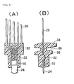
- Fig. 3 is a schematic view showing a thin-film sensor module (for example, a temperature sensor module) according to an embodiment of the present invention.
- Fig. 4 is a set of schematic sectional views illustrating a thin-film sensor module (for example, a temperature sensor module) according to an embodiment of the present invention, wherein (a) is a longitudinal sectional plane view and (b) is a longitudinal sectional side view.
- a thin-film sensor module (for example, a temperature sensor module) 20 of the invention has and a thin-film sensor (for example, a temperature sensor) 10 to which a fin plate 24 and output terminals 26 are firmly bonded inside a housing 22.
- the housing 22 may be made of any material having low thermal conductivity. Materials resistant to chemicals or oils may be used depending on the type of the sample object or fluid. Examples of the materials having these properties include epoxy resins, polybutylene terephthalate (PBT) and polyphenylene sulfide (PPS).
- the thin-film sensor module may have various shapes depending on the application of the thin-film sensor module. For example, the housing 22 as shown in Figs.
- 3 and 4 (B) has a first large-diameter part 34 from which the output terminals 26 protrude, and a second large-diameter part 36 below the first large-diameter part 34 with a spacing therebetween; and may have a notch 38 that provides a heat insulating space between the first large-diameter part 34 and the second large-diameter part 36.
- the shape of the housing 22 is not limited to that described above.
- the fin plate 24 may be made of any material without limitation as long as it has good thermal conductivity. Examples of the materials include copper, aluminum, tungsten, duralumin and copper-tungsten alloy.
- the fin plate 24 may have various shapes depending on the application of the thin-film sensor module. For example, it may be a thin plate having a thickness of approximately 200 ⁇ m.
- the fin plate 24 and the thin-film sensor 10 may be firmly bonded together with any thermally conductive material such as silver paste.
- the output terminals 26 may be made of any material without limitation as long as the material has electrical conductivity. Examples of the materials include copper and aluminum.
- the output terminals 26 may be electrically connected to the thin-film sensor 10 via bonding wires 32.
- the output terminals 26 extending from the resin housing 2 are arranged in a straight line and gradually increase (or gradually reduce) the length in which they extend from the resin housing 2 from one end to the other of the straight line.
- the output terminals 26 may have various shapes depending on application.
- the shape shown in Fig. 3 permits easy attachment of a sensor pressing plate that presses downward the thin-film sensor module 20, or a flow rate-detecting circuit board that forms a circuit by being connected with the output terminals 26.
- the shape shown in the figure also reduces the probability that the thin-film sensor module 20 will be damaged during the attaching of the sensor pressing plate or the flow rate-detecting circuit board.
- a SiO 2 layer with a thickness of 300 nm was formed on an alumina substrate (a circular disk 100 mm in diameter and 385 ⁇ m in thickness) by spin coating under the following conditions.
- a titanium layer having a thickness of 30 nm was formed bv sputtering using metal titanium (99.99% purity) as the target under the following conditions.
- an electrical resistor having a thickness of 400 nm was formed by sputtering using platinum (99.9% purity) as the target under the following conditions.
- the thin-film sensor 1 produced as described above was tested for temperature coefficient of resistance (TCR), crystal grain diameters, orientation properties, adhesion, Ra and Rz as described later. The results are set forth in Table 1.
- a SiO 2 layer and a titanium layer were formed on an alumina substrate in the same manner as in Comparative Example 1.
- an electrical resistor having a thickness of 400 nm was formed by sputtering using platinum (99.9% purity) as the target under the following conditions.
- a thin-film sensor 2 was thus manufactured.
- the thin-film sensor 2 produced as described above was tested for temperature coefficient of resistance (TCR), crystal grain diameters, orientation properties, adhesion, Ra and Rz as described later. The results are set forth in Table 1.
- a thin-film sensor 3 was produced in the same manner as in Example 1 except that the direct-current voltage in Example 1 was changed to -50 V.
- the thin-film sensor 3 was tested for temperature coefficient of resistance (TCR), crystal grain diameters, orientation properties, adhesion, Ra and Rz as described later. The results are set forth in Table 1.
- the thin-film sensor 1 produced in Comparative Example 1 was heat treated at 1,000°C for 4 hours in an air atmosphere to give a thin-film sensor 4.
- the thin-film sensor 4 was tested for temperature coefficient of resistance (TCR), crystal grain diameters, orientation properties, adhesion, Ra and Rz as described later. The results are set forth in Table 1.
- TCR temperature coefficient of resistance
- the thin-film sensor was tested for specific electric resistance p at varied temperatures, and the temperature coefficient of resistance (TCR) was obtained from the results.
- the temperature coefficient of resistance is expressed by Formula 1 below.
- a longitudinal section of the thin-film sensor was smoothed by polishing and with focused ion beam (FIB).
- image data of the crystal pattern was obtained by EBSD method by means of a scanning electron microscope (JSM-6700F or JSM-7000F manufactured by JEOL Ltd.) that had a FE gun and was equipped with an EBSD apparatus (OIM Analysis, manufactured by TSL Solutions) and also by means of the supplied EBSD analyzer.
- the image data was analyzed while selecting "Grain Size" from the analysis menu of an EBSD analysis program (OIM Analysis, the same as above), and the grain diameters ( ⁇ m) of crystal grains having a crystal rotation angle of 5° or more were measured. In the determination of the crystal grain diameters, ⁇ 3 grain boundaries indicating twin boundaries were considered as intragranular defects.
- a longitudianal section of the thin-film sensor was smoothed by polishing and with focused ion beam (FIB).
- image data of the crystal pattern was obtained by EBSD method by means of a scanning electron microscope (JSM-6700F or JSM-7000F manufactured by JEOL Ltd.) that had a FE gun and was equipped with an EBSD apparatus (OIM Analysis, manufactured by TSL Solutions) and also by means of the supplied EBSD analyzer.
- the image data was analyzed while selecting "Crystal Direction" from the analysis menu of an EBSD analysis program (OIM Analysis, the same as above), under conditions such that the percentage relative to the total crystal grains was obtained of crystal grains wherein the plane direction of (111) planes of the platinum crystal of the electrical resistor was misaligned by not more than 10 degrees from the normal direction (ND) of the multilayer structure or the thin-film sensor.
- the percentage was defined as the orientation properties. Crystal grains having a crystal rotation angle of 5° or more were recognized to have crystal boundaries with each other, and crystal grains having a crystal rotation angle of less than 5° were collectively recognized as one crystal grain.
- the surface roughness Ra and Rz of the thin-film sensor were measured with an optical interferometric three-dimensional structural analysis microscope (New View 5032, manufactured by Zygo Corporation). An area 54 x 72 ⁇ m in size was observed with a x100 Mirau lens using white light. The surface roughness Ra and Rz were determined from the three-dimensional image of the observed surface.
- the thin-film sensor was tested for adhesion between the insulating substrate and the electrical resistor by the following wire pull test.
- a gold wire (25 ⁇ m in diameter) was bonded to the gold electrode pad (18) of the thin-film chip (thin-film sensor). The gold wire was pulled with a load of about 10 g in the vertical direction relative to the thin-film chip at room temperature.
- the evaluation criteria were as follows.
- AA The gold electrode pad and the electrical resistor were not peeled from the gold wire, and the gold wire was broken.
- CC The gold electrode pad and the electrical resistor were peeled from the gold wire.
Landscapes
- Engineering & Computer Science (AREA)
- Physics & Mathematics (AREA)
- General Physics & Mathematics (AREA)
- Spectroscopy & Molecular Physics (AREA)
- Microelectronics & Electronic Packaging (AREA)
- Manufacturing & Machinery (AREA)
- Electromagnetism (AREA)
- Measuring Volume Flow (AREA)
- Thermistors And Varistors (AREA)
Applications Claiming Priority (2)
| Application Number | Priority Date | Filing Date | Title |
|---|---|---|---|
| JP2006088415 | 2006-03-28 | ||
| PCT/JP2007/056589 WO2007114143A1 (fr) | 2006-03-28 | 2007-03-28 | Procede de fabrication de capteur a film mince, capteur a film mince et module de capteur a film mince |
Publications (1)
| Publication Number | Publication Date |
|---|---|
| EP2009647A1 true EP2009647A1 (fr) | 2008-12-31 |
Family
ID=38563412
Family Applications (1)
| Application Number | Title | Priority Date | Filing Date |
|---|---|---|---|
| EP07740027A Withdrawn EP2009647A1 (fr) | 2006-03-28 | 2007-03-28 | Procede de fabrication de capteur a film mince, capteur a film mince et module de capteur a film mince |
Country Status (3)
| Country | Link |
|---|---|
| US (1) | US20100245030A1 (fr) |
| EP (1) | EP2009647A1 (fr) |
| WO (1) | WO2007114143A1 (fr) |
Cited By (2)
| Publication number | Priority date | Publication date | Assignee | Title |
|---|---|---|---|---|
| EP2914957A4 (fr) * | 2012-10-30 | 2016-06-15 | Edwards Lifesciences Corp | Capteur d'analyte et procédés de fabrication |
| EP2959932A4 (fr) * | 2013-02-22 | 2017-05-03 | Yong Il Cho | Module de dispositif chauffant pour dispositif de chauffage d'appareil de perfusion de liquide et son procédé de fabrication |
Families Citing this family (8)
| Publication number | Priority date | Publication date | Assignee | Title |
|---|---|---|---|---|
| US8465812B2 (en) * | 2009-03-23 | 2013-06-18 | The Boeing Company | Durable transparent intelligent coatings for polymeric transparencies |
| JP5477767B2 (ja) * | 2009-11-16 | 2014-04-23 | 三菱マテリアル株式会社 | 硬質被覆層がすぐれた耐チッピング性を発揮する表面被覆切削工具 |
| JPWO2012086529A1 (ja) * | 2010-12-22 | 2014-05-22 | 株式会社マーレ フィルターシステムズ | キャニスタの検出装置 |
| US9963777B2 (en) * | 2012-10-08 | 2018-05-08 | Analog Devices, Inc. | Methods of forming a thin film resistor |
| US9982900B2 (en) | 2014-01-29 | 2018-05-29 | Trane International Inc. | Method of attaching electrodes to plated thermoset plastic heated blower housing |
| US9972425B2 (en) * | 2015-06-30 | 2018-05-15 | Qorvo Us, Inc. | Frequency-dependent resistor and circuitry employing the same |
| CN112136022A (zh) * | 2018-05-16 | 2020-12-25 | 山特维克材料技术公司 | 具有传感器布置结构的金属管结构 |
| JP7406517B2 (ja) * | 2020-03-24 | 2023-12-27 | ミネベアミツミ株式会社 | ひずみゲージ |
Family Cites Families (12)
| Publication number | Priority date | Publication date | Assignee | Title |
|---|---|---|---|---|
| US4533605A (en) * | 1980-09-09 | 1985-08-06 | Westinghouse Electric Corp. | Article such as jewelry or a wristwatch component having composite multi-film protective coating |
| US4624137A (en) * | 1981-10-09 | 1986-11-25 | Honeywell Inc. | Semiconductor device |
| JPS5922399B2 (ja) * | 1981-10-14 | 1984-05-26 | 日本電気株式会社 | 多層セラミツク基板 |
| JPS61188901A (ja) * | 1985-02-16 | 1986-08-22 | 株式会社日本自動車部品総合研究所 | 流量センサ用膜式抵抗 |
| JP2758602B2 (ja) * | 1987-12-29 | 1998-05-28 | 日本電気株式会社 | 磁気記録媒体およびその製造方法 |
| US4952904A (en) * | 1988-12-23 | 1990-08-28 | Honeywell Inc. | Adhesion layer for platinum based sensors |
| JPH11354302A (ja) | 1998-06-09 | 1999-12-24 | Mitsui Mining & Smelting Co Ltd | 薄膜抵抗素子 |
| CA2375322A1 (fr) * | 1999-06-24 | 2000-12-28 | Mitsui Mining & Smelting Co., Ltd. | Detecteur de debit, debitmetre et capteur de flux |
| JP2001091321A (ja) * | 1999-09-21 | 2001-04-06 | Mitsui Mining & Smelting Co Ltd | 流量センサーユニット及びこれを用いた流量計 |
| JP2001012982A (ja) * | 1999-06-29 | 2001-01-19 | Mitsui Mining & Smelting Co Ltd | 流量センサー及び温度センサー |
| JP2001291607A (ja) | 2000-04-04 | 2001-10-19 | Mitsui Mining & Smelting Co Ltd | 白金薄膜抵抗体の製造方法 |
| JP5138134B2 (ja) * | 2001-07-16 | 2013-02-06 | 株式会社デンソー | 薄膜式センサの製造方法ならびにフローセンサの製造方法 |
-
2007
- 2007-03-28 EP EP07740027A patent/EP2009647A1/fr not_active Withdrawn
- 2007-03-28 WO PCT/JP2007/056589 patent/WO2007114143A1/fr not_active Ceased
- 2007-03-28 US US12/294,849 patent/US20100245030A1/en not_active Abandoned
Non-Patent Citations (1)
| Title |
|---|
| See references of WO2007114143A1 * |
Cited By (2)
| Publication number | Priority date | Publication date | Assignee | Title |
|---|---|---|---|---|
| EP2914957A4 (fr) * | 2012-10-30 | 2016-06-15 | Edwards Lifesciences Corp | Capteur d'analyte et procédés de fabrication |
| EP2959932A4 (fr) * | 2013-02-22 | 2017-05-03 | Yong Il Cho | Module de dispositif chauffant pour dispositif de chauffage d'appareil de perfusion de liquide et son procédé de fabrication |
Also Published As
| Publication number | Publication date |
|---|---|
| WO2007114143A1 (fr) | 2007-10-11 |
| US20100245030A1 (en) | 2010-09-30 |
Similar Documents
| Publication | Publication Date | Title |
|---|---|---|
| EP2009647A1 (fr) | Procede de fabrication de capteur a film mince, capteur a film mince et module de capteur a film mince | |
| US20090174520A1 (en) | Laminates, Thin-Film Sensors, Thin-Film Sensor Modules, and Methods for Producing the Thin-Film Sensors | |
| KR101024801B1 (ko) | 온도 측정 부재, 온도 측정 장치 및 온도 측정 방법 | |
| EP3690385B1 (fr) | Jauge de contrainte et module de capteur | |
| TWI382428B (zh) | Touch panel sensor | |
| US10564049B2 (en) | Copper thermal resistance thin film temperature sensor chip, and preparation method therefor | |
| US9150955B2 (en) | Method of making molybdenum containing targets comprising molybdenum, titanium, and tantalum or chromium | |
| CN104508442B (zh) | 温度传感器 | |
| CN111417831B (zh) | 应变片 | |
| US4805296A (en) | Method of manufacturing platinum resistance thermometer | |
| JP6108156B2 (ja) | 温度センサ | |
| CN119213902A (zh) | 压电层叠体、压电元件和压电层叠体的制造方法 | |
| TW202119436A (zh) | 導電膜、導電膜捲繞體及其製造方法、以及溫度感測膜 | |
| US10465275B2 (en) | Iron bus bar having copper layer, and method for manufacturing the same | |
| JP2007294870A (ja) | 薄膜センサ、薄膜センサモジュールおよび薄膜センサの製造方法 | |
| JP6052614B2 (ja) | 温度センサ | |
| KR100393945B1 (ko) | 금속 박막 저항체 소자의 제조 방법 및 이를 이용한 금속 박막 온도 센서의 제조 방법 | |
| JP2007243173A (ja) | 積層体、薄膜センサ及び薄膜センサモジュール | |
| JPWO2008143011A1 (ja) | 薄膜センサ、薄膜センサモジュールおよび薄膜センサの製造方法 | |
| KR101597018B1 (ko) | 금속 박막 및 금속 박막 형성용 Mo 합금 스퍼터링 타깃재 | |
| JP2007300065A (ja) | 薄膜センサ、薄膜センサモジュール及び薄膜センサの製造方法 | |
| JP2013211180A (ja) | 温度センサ付きフィルムヒータ | |
| JP2007294929A (ja) | 薄膜センサの製造方法、薄膜センサおよび薄膜センサモジュール | |
| CN117099172A (zh) | 应变电阻膜、压力传感器及层叠体 | |
| US20240339380A1 (en) | Semiconductor-type wind speed sensor and method of manufacturing the same |
Legal Events
| Date | Code | Title | Description |
|---|---|---|---|
| PUAI | Public reference made under article 153(3) epc to a published international application that has entered the european phase |
Free format text: ORIGINAL CODE: 0009012 |
|
| 17P | Request for examination filed |
Effective date: 20081016 |
|
| AK | Designated contracting states |
Kind code of ref document: A1 Designated state(s): AT BE BG CH CY CZ DE DK EE ES FI FR GB GR HU IE IS IT LI LT LU LV MC MT NL PL PT RO SE SI SK TR |
|
| AX | Request for extension of the european patent |
Extension state: AL BA HR MK RS |
|
| STAA | Information on the status of an ep patent application or granted ep patent |
Free format text: STATUS: THE APPLICATION HAS BEEN WITHDRAWN |
|
| 18W | Application withdrawn |
Effective date: 20110831 |