EP2009693A1 - Herstellungsverfahren eines gesischerten elektronischen System, entsprechende Vorrichtung zur Schützen von einer integrierten Schaltung und entsprechendes elektronisches System - Google Patents
Herstellungsverfahren eines gesischerten elektronischen System, entsprechende Vorrichtung zur Schützen von einer integrierten Schaltung und entsprechendes elektronisches System Download PDFInfo
- Publication number
- EP2009693A1 EP2009693A1 EP07301186A EP07301186A EP2009693A1 EP 2009693 A1 EP2009693 A1 EP 2009693A1 EP 07301186 A EP07301186 A EP 07301186A EP 07301186 A EP07301186 A EP 07301186A EP 2009693 A1 EP2009693 A1 EP 2009693A1
- Authority
- EP
- European Patent Office
- Prior art keywords
- electrical
- integrated circuit
- circuit
- network
- image
- Prior art date
- Legal status (The legal status is an assumption and is not a legal conclusion. Google has not performed a legal analysis and makes no representation as to the accuracy of the status listed.)
- Withdrawn
Links
Images


Classifications
-
- H—ELECTRICITY
- H10—SEMICONDUCTOR DEVICES; ELECTRIC SOLID-STATE DEVICES NOT OTHERWISE PROVIDED FOR
- H10W—GENERIC PACKAGES, INTERCONNECTIONS, CONNECTORS OR OTHER CONSTRUCTIONAL DETAILS OF DEVICES COVERED BY CLASS H10
- H10W42/00—Arrangements for protection of devices
- H10W42/40—Arrangements for protection of devices protecting against tampering, e.g. unauthorised inspection or reverse engineering
- H10W42/405—Arrangements for protection of devices protecting against tampering, e.g. unauthorised inspection or reverse engineering using active circuits
-
- G—PHYSICS
- G06—COMPUTING OR CALCULATING; COUNTING
- G06F—ELECTRIC DIGITAL DATA PROCESSING
- G06F21/00—Security arrangements for protecting computers, components thereof, programs or data against unauthorised activity
- G06F21/70—Protecting specific internal or peripheral components, in which the protection of a component leads to protection of the entire computer
- G06F21/86—Secure or tamper-resistant housings
- G06F21/87—Secure or tamper-resistant housings by means of encapsulation, e.g. for integrated circuits
-
- H—ELECTRICITY
- H10—SEMICONDUCTOR DEVICES; ELECTRIC SOLID-STATE DEVICES NOT OTHERWISE PROVIDED FOR
- H10W—GENERIC PACKAGES, INTERCONNECTIONS, CONNECTORS OR OTHER CONSTRUCTIONAL DETAILS OF DEVICES COVERED BY CLASS H10
- H10W90/00—Package configurations
-
- G—PHYSICS
- G06—COMPUTING OR CALCULATING; COUNTING
- G06F—ELECTRIC DIGITAL DATA PROCESSING
- G06F2221/00—Indexing scheme relating to security arrangements for protecting computers, components thereof, programs or data against unauthorised activity
- G06F2221/21—Indexing scheme relating to G06F21/00 and subgroups addressing additional information or applications relating to security arrangements for protecting computers, components thereof, programs or data against unauthorised activity
- G06F2221/2143—Clearing memory, e.g. to prevent the data from being stolen
-
- H—ELECTRICITY
- H10—SEMICONDUCTOR DEVICES; ELECTRIC SOLID-STATE DEVICES NOT OTHERWISE PROVIDED FOR
- H10W—GENERIC PACKAGES, INTERCONNECTIONS, CONNECTORS OR OTHER CONSTRUCTIONAL DETAILS OF DEVICES COVERED BY CLASS H10
- H10W70/00—Package substrates; Interposers; Redistribution layers [RDL]
- H10W70/60—Insulating or insulated package substrates; Interposers; Redistribution layers
- H10W70/62—Insulating or insulated package substrates; Interposers; Redistribution layers characterised by their interconnections
- H10W70/65—Shapes or dispositions of interconnections
- H10W70/654—Top-view layouts
- H10W70/655—Fan-out layouts
-
- H—ELECTRICITY
- H10—SEMICONDUCTOR DEVICES; ELECTRIC SOLID-STATE DEVICES NOT OTHERWISE PROVIDED FOR
- H10W—GENERIC PACKAGES, INTERCONNECTIONS, CONNECTORS OR OTHER CONSTRUCTIONAL DETAILS OF DEVICES COVERED BY CLASS H10
- H10W90/00—Package configurations
- H10W90/701—Package configurations characterised by the relative positions of pads or connectors relative to package parts
- H10W90/721—Package configurations characterised by the relative positions of pads or connectors relative to package parts of bump connectors
- H10W90/722—Package configurations characterised by the relative positions of pads or connectors relative to package parts of bump connectors between stacked chips
Definitions
- Electrical connection pads allow the securing circuit 1 in particular to exchange, with the outside, through a bi-directional communication bus 19, various input / output signals.
- the memory or memories 12 are internal to the security circuit 1. According to a variant (not shown), such memories are provided, for example, within the circuit to be secured.
- the memory or memories 12 include, for example, a nonvolatile type memory, for example of the flash type intended to save data permanently, that is to say that remain despite one or more extinctions of the power supply.
- the nonvolatile memory 12 is in particular designed to store data specific to any electrical image relating to the existing network of electrical connections 14 during its capture, including the electrical reference image and at least the last captured electrical image. following the commissioning of the circuit to be secured.
- the memory 12 also comprises one or more instruction programs used to initialize and configure the communication to be established between the security circuit 1 and the circuit to be secured.
- the re-routing provides an additional degree of freedom, in order to re-position connection pads at desired locations including either to prohibit their access from outside the system formed, or on the contrary to allow access from outside the formed system.
- the integrated circuit to secure performs at least one function, for example, provide high speed data communication, USB type (acronym for "Universal Serial Bus” in English), type MMC (acronym for "Multi-Media CArd” In English) and / or equivalent.
- such a method allows the system formed by the two coupled circuits to capture, in addition to the electrical reference image captured during its manufacture, at least one other electrical image. It can be an electrical image captured at regular intervals, for example, every second, as soon as the system is put into operation.
- a periodic and permanent check of the state or the integrity of the electrical connection network of the secure system during operation can be carried out.
- the security circuit carrying the network and can be autonomous to detect tampering or non-alteration of the electrical image of the network is active during operation of the system formed.
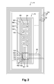
- the securing device 1 comprises a first silicon substrate 52 carrying the active part of the securing circuit 44 and the protection grid 42 connecting the emitters and the receivers together.
- the protective grid 42 completely covers the active part of the security circuit 44 and at least partially the first silicon substrate 52.
- an active part of the security circuit 44 it is necessary in particular to include a microprocessor and / or a logic unit that manages and controls the capture of an electrical reference image and any electrical image captured later.
- the active part of the securing circuit 44 covers, for its part, the connection pads 46 that are inaccessible from outside the secure electronic system 50.
- the protection grid 42 is in the same plane as the connection pads 46 of the circuit. security 44.
- the active portion 510 overcomes a second silicon substrate 54 carrying the circuit to be secured 512.
Landscapes
- Engineering & Computer Science (AREA)
- Computer Hardware Design (AREA)
- Theoretical Computer Science (AREA)
- Microelectronics & Electronic Packaging (AREA)
- Computer Security & Cryptography (AREA)
- Software Systems (AREA)
- Physics & Mathematics (AREA)
- General Engineering & Computer Science (AREA)
- General Physics & Mathematics (AREA)
- Storage Device Security (AREA)
Priority Applications (4)
| Application Number | Priority Date | Filing Date | Title |
|---|---|---|---|
| EP07301186A EP2009693A1 (de) | 2007-06-29 | 2007-06-29 | Herstellungsverfahren eines gesischerten elektronischen System, entsprechende Vorrichtung zur Schützen von einer integrierten Schaltung und entsprechendes elektronisches System |
| PCT/EP2008/058034 WO2009003879A1 (fr) | 2007-06-29 | 2008-06-24 | Procédé de fabrication d'un système électronique sécurisé, dispositif de sécurisation de circuit intégré et système électronique correspondants |
| KR1020107002029A KR101105911B1 (ko) | 2007-06-29 | 2008-06-24 | 보안 보호 전자 시스템 제조 방법, 이에 대응하는 집적 회로 보안 보호 장치, 및 이에 대응하는 전자 시스템 |
| EP08761341A EP2162913A1 (de) | 2007-06-29 | 2008-06-24 | Verfahren zur herstellung eines sicherheitsgeschützten elektronischen systems, entsprechende sicherheitsschutzeinrichtung integrierter schaltungen und entsprechendes elektronisches system |
Applications Claiming Priority (1)
| Application Number | Priority Date | Filing Date | Title |
|---|---|---|---|
| EP07301186A EP2009693A1 (de) | 2007-06-29 | 2007-06-29 | Herstellungsverfahren eines gesischerten elektronischen System, entsprechende Vorrichtung zur Schützen von einer integrierten Schaltung und entsprechendes elektronisches System |
Publications (1)
| Publication Number | Publication Date |
|---|---|
| EP2009693A1 true EP2009693A1 (de) | 2008-12-31 |
Family
ID=38973063
Family Applications (2)
| Application Number | Title | Priority Date | Filing Date |
|---|---|---|---|
| EP07301186A Withdrawn EP2009693A1 (de) | 2007-06-29 | 2007-06-29 | Herstellungsverfahren eines gesischerten elektronischen System, entsprechende Vorrichtung zur Schützen von einer integrierten Schaltung und entsprechendes elektronisches System |
| EP08761341A Withdrawn EP2162913A1 (de) | 2007-06-29 | 2008-06-24 | Verfahren zur herstellung eines sicherheitsgeschützten elektronischen systems, entsprechende sicherheitsschutzeinrichtung integrierter schaltungen und entsprechendes elektronisches system |
Family Applications After (1)
| Application Number | Title | Priority Date | Filing Date |
|---|---|---|---|
| EP08761341A Withdrawn EP2162913A1 (de) | 2007-06-29 | 2008-06-24 | Verfahren zur herstellung eines sicherheitsgeschützten elektronischen systems, entsprechende sicherheitsschutzeinrichtung integrierter schaltungen und entsprechendes elektronisches system |
Country Status (3)
| Country | Link |
|---|---|
| EP (2) | EP2009693A1 (de) |
| KR (1) | KR101105911B1 (de) |
| WO (1) | WO2009003879A1 (de) |
Citations (6)
| Publication number | Priority date | Publication date | Assignee | Title |
|---|---|---|---|---|
| WO1997022990A1 (en) * | 1995-12-20 | 1997-06-26 | Intel Corporation | Secure semiconductor device |
| US5877547A (en) * | 1994-11-17 | 1999-03-02 | Schlumberger Industries | Active security device including an electronic memory |
| US6438825B1 (en) * | 1995-03-28 | 2002-08-27 | Intel Corporation | Method to prevent intrusions into electronic circuitry |
| US20030008432A1 (en) * | 1999-05-03 | 2003-01-09 | Andreas Kux | Method and device for securing a multi-dimensionally constructed chip stack and chip configuration |
| EP1432031A1 (de) * | 2002-12-20 | 2004-06-23 | Lipman Electronic Engineering Ltd. | Gehäuse mit Einbruchschutz für elektronische Schaltungen |
| US20040193877A1 (en) * | 2001-07-12 | 2004-09-30 | Thomas Grassl | Portable data carrier assembly comprising a security device |
Family Cites Families (1)
| Publication number | Priority date | Publication date | Assignee | Title |
|---|---|---|---|---|
| JPS6130059A (ja) | 1984-07-20 | 1986-02-12 | Nec Corp | 半導体装置の製造方法 |
-
2007
- 2007-06-29 EP EP07301186A patent/EP2009693A1/de not_active Withdrawn
-
2008
- 2008-06-24 KR KR1020107002029A patent/KR101105911B1/ko not_active Expired - Fee Related
- 2008-06-24 WO PCT/EP2008/058034 patent/WO2009003879A1/fr not_active Ceased
- 2008-06-24 EP EP08761341A patent/EP2162913A1/de not_active Withdrawn
Patent Citations (6)
| Publication number | Priority date | Publication date | Assignee | Title |
|---|---|---|---|---|
| US5877547A (en) * | 1994-11-17 | 1999-03-02 | Schlumberger Industries | Active security device including an electronic memory |
| US6438825B1 (en) * | 1995-03-28 | 2002-08-27 | Intel Corporation | Method to prevent intrusions into electronic circuitry |
| WO1997022990A1 (en) * | 1995-12-20 | 1997-06-26 | Intel Corporation | Secure semiconductor device |
| US20030008432A1 (en) * | 1999-05-03 | 2003-01-09 | Andreas Kux | Method and device for securing a multi-dimensionally constructed chip stack and chip configuration |
| US20040193877A1 (en) * | 2001-07-12 | 2004-09-30 | Thomas Grassl | Portable data carrier assembly comprising a security device |
| EP1432031A1 (de) * | 2002-12-20 | 2004-06-23 | Lipman Electronic Engineering Ltd. | Gehäuse mit Einbruchschutz für elektronische Schaltungen |
Also Published As
| Publication number | Publication date |
|---|---|
| EP2162913A1 (de) | 2010-03-17 |
| KR20100025587A (ko) | 2010-03-09 |
| WO2009003879A1 (fr) | 2009-01-08 |
| KR101105911B1 (ko) | 2012-01-17 |
Similar Documents
| Publication | Publication Date | Title |
|---|---|---|
| EP0481881B1 (de) | Integrierte Schaltung für verbesserten Zugang | |
| WO2012089983A1 (fr) | Procédé et dispositif de contrôle d'accès à un système informatique | |
| US10318462B2 (en) | Secure crypto module including optical glass security layer | |
| FR2746962A1 (fr) | Dispositif de securite d'une pastille semi-conductrice | |
| EP2735969A1 (de) | Elektronische Einheit, die ein Deaktivierungsmodul umfasst | |
| FR2979442A1 (fr) | Microprocesseur protege contre le vidage de memoire | |
| EP2241997B1 (de) | Speicherkartenleser | |
| FR2730328A1 (fr) | Connecteur pour appareil lecteur de carte a microcircuit et appareil lecteur de carte a microcircuit le comprenant | |
| EP3371735B1 (de) | Körper eines speicherkartenlesers mit einem schutznetz auf beiden seiten | |
| WO2003077194A2 (fr) | Dispositif electronique securise | |
| EP2431901A1 (de) | Schutzvorrichtung, Verfahren und entsprechendes Computerprogramm | |
| EP2009693A1 (de) | Herstellungsverfahren eines gesischerten elektronischen System, entsprechende Vorrichtung zur Schützen von einer integrierten Schaltung und entsprechendes elektronisches System | |
| FR3052571A1 (fr) | Procede de calibration d'une horloge d'un circuit de carte a puce, et systeme associe | |
| US10430615B2 (en) | Secure crypto module including optical security pathway | |
| EP1006532B1 (de) | Sicherer EEPROM-Speicher mit UV-Lösch-Erkennungsmitteln | |
| FR2824648A1 (fr) | Procede de protection d'un circuit logique contre des attaques exterieures, et unite logique contenant un circuit logique a proteger contre des attaques exterieures | |
| CA2575143A1 (fr) | Procede et dispositif de traitement de donnees | |
| EP2680184A1 (de) | Integrierter Schaltkreis, der gegen aktive Angriffe von Piraten geschützt ist | |
| EP3350745B1 (de) | Verwaltung einer anzeige einer ansicht einer anwendung auf einem schirm einer elektronischen dateneingabevorrichtung, entsprechendes verfahren, vorrichtung und computerprogrammprodukt | |
| EP3107358A1 (de) | Komponente zum schutz von sensiblen signalen, vorrichtung und entsprechendes verfahren | |
| FR2892544A1 (fr) | Detection de tentative d'effraction sur une puce a travers sa structure support | |
| FR2957443A1 (fr) | Carte a microcircuit(s) avec contremesure pour attaques en faute par rayonnement lumineux | |
| EP2564600B1 (de) | Verfahren zur detektion einer abnormalen betrieblichen umgebungsbedingung eines in einer vorrichtung eingebetteten elements sowie zugehöriges element | |
| FR3124287A1 (fr) | Procédé et dispositif de contrôle d’accès à un support de stockage. | |
| FR2880972A1 (fr) | Dispositif anti-piratage de securisation et/ou de protection d'appareils formes d'une pluralite de composants electroniques |
Legal Events
| Date | Code | Title | Description |
|---|---|---|---|
| PUAI | Public reference made under article 153(3) epc to a published international application that has entered the european phase |
Free format text: ORIGINAL CODE: 0009012 |
|
| AK | Designated contracting states |
Kind code of ref document: A1 Designated state(s): AT BE BG CH CY CZ DE DK EE ES FI FR GB GR HU IE IS IT LI LT LU LV MC MT NL PL PT RO SE SI SK TR |
|
| AX | Request for extension of the european patent |
Extension state: AL BA HR MK RS |
|
| STAA | Information on the status of an ep patent application or granted ep patent |
Free format text: STATUS: THE APPLICATION HAS BEEN WITHDRAWN |
|
| 18W | Application withdrawn |
Effective date: 20090616 |