EP2009699A2 - Structures supramoléculaires et dispositifs les comprenant - Google Patents
Structures supramoléculaires et dispositifs les comprenant Download PDFInfo
- Publication number
- EP2009699A2 EP2009699A2 EP08017802A EP08017802A EP2009699A2 EP 2009699 A2 EP2009699 A2 EP 2009699A2 EP 08017802 A EP08017802 A EP 08017802A EP 08017802 A EP08017802 A EP 08017802A EP 2009699 A2 EP2009699 A2 EP 2009699A2
- Authority
- EP
- European Patent Office
- Prior art keywords
- atom
- atoms
- type
- host
- dopant
- Prior art date
- Legal status (The legal status is an assumption and is not a legal conclusion. Google has not performed a legal analysis and makes no representation as to the accuracy of the status listed.)
- Granted
Links
- 239000002019 doping agent Substances 0.000 claims abstract description 111
- 239000000463 material Substances 0.000 claims abstract description 35
- 230000010355 oscillation Effects 0.000 claims abstract description 29
- 239000012535 impurity Substances 0.000 claims abstract description 19
- 230000004044 response Effects 0.000 claims abstract description 3
- 230000004888 barrier function Effects 0.000 claims description 17
- 125000004429 atom Chemical group 0.000 description 132
- 210000004027 cell Anatomy 0.000 description 82
- 239000004065 semiconductor Substances 0.000 description 43
- 239000000370 acceptor Substances 0.000 description 35
- 239000000758 substrate Substances 0.000 description 34
- 238000000034 method Methods 0.000 description 32
- 239000010408 film Substances 0.000 description 27
- 238000004519 manufacturing process Methods 0.000 description 20
- 238000009826 distribution Methods 0.000 description 18
- XUIMIQQOPSSXEZ-UHFFFAOYSA-N Silicon Chemical group [Si] XUIMIQQOPSSXEZ-UHFFFAOYSA-N 0.000 description 16
- 230000000694 effects Effects 0.000 description 15
- 229910052710 silicon Inorganic materials 0.000 description 15
- 239000010703 silicon Substances 0.000 description 15
- 239000000523 sample Substances 0.000 description 14
- 238000001451 molecular beam epitaxy Methods 0.000 description 11
- 238000003491 array Methods 0.000 description 10
- 230000006870 function Effects 0.000 description 9
- 239000011159 matrix material Substances 0.000 description 9
- 230000001427 coherent effect Effects 0.000 description 8
- 230000008569 process Effects 0.000 description 8
- 238000000059 patterning Methods 0.000 description 7
- 239000010410 layer Substances 0.000 description 6
- 230000008859 change Effects 0.000 description 4
- 238000005229 chemical vapour deposition Methods 0.000 description 4
- 238000000151 deposition Methods 0.000 description 4
- VYPSYNLAJGMNEJ-UHFFFAOYSA-N Silicium dioxide Chemical compound O=[Si]=O VYPSYNLAJGMNEJ-UHFFFAOYSA-N 0.000 description 3
- WUKWITHWXAAZEY-UHFFFAOYSA-L calcium difluoride Chemical compound [F-].[F-].[Ca+2] WUKWITHWXAAZEY-UHFFFAOYSA-L 0.000 description 3
- 229910001634 calcium fluoride Inorganic materials 0.000 description 3
- 238000005516 engineering process Methods 0.000 description 3
- 238000001459 lithography Methods 0.000 description 3
- 230000007246 mechanism Effects 0.000 description 3
- 238000000926 separation method Methods 0.000 description 3
- 239000002356 single layer Substances 0.000 description 3
- 239000007787 solid Substances 0.000 description 3
- 238000012546 transfer Methods 0.000 description 3
- ZOXJGFHDIHLPTG-UHFFFAOYSA-N Boron Chemical group [B] ZOXJGFHDIHLPTG-UHFFFAOYSA-N 0.000 description 2
- 101100285518 Drosophila melanogaster how gene Proteins 0.000 description 2
- 238000003877 atomic layer epitaxy Methods 0.000 description 2
- 230000005540 biological transmission Effects 0.000 description 2
- 229910052796 boron Inorganic materials 0.000 description 2
- 210000000349 chromosome Anatomy 0.000 description 2
- 229910052681 coesite Inorganic materials 0.000 description 2
- 229910052906 cristobalite Inorganic materials 0.000 description 2
- 238000013461 design Methods 0.000 description 2
- 238000001312 dry etching Methods 0.000 description 2
- 229910052739 hydrogen Inorganic materials 0.000 description 2
- 239000001257 hydrogen Substances 0.000 description 2
- 125000004435 hydrogen atom Chemical group [H]* 0.000 description 2
- 230000004048 modification Effects 0.000 description 2
- 238000012986 modification Methods 0.000 description 2
- 230000003534 oscillatory effect Effects 0.000 description 2
- 238000002161 passivation Methods 0.000 description 2
- 125000004437 phosphorous atom Chemical group 0.000 description 2
- 229910052698 phosphorus Inorganic materials 0.000 description 2
- 239000011148 porous material Substances 0.000 description 2
- 108090000623 proteins and genes Proteins 0.000 description 2
- 102000004169 proteins and genes Human genes 0.000 description 2
- 239000000377 silicon dioxide Substances 0.000 description 2
- 229910052682 stishovite Inorganic materials 0.000 description 2
- 239000000126 substance Substances 0.000 description 2
- 230000007704 transition Effects 0.000 description 2
- 229910052905 tridymite Inorganic materials 0.000 description 2
- OKTJSMMVPCPJKN-UHFFFAOYSA-N Carbon Chemical compound [C] OKTJSMMVPCPJKN-UHFFFAOYSA-N 0.000 description 1
- OAICVXFJPJFONN-UHFFFAOYSA-N Phosphorus Chemical compound [P] OAICVXFJPJFONN-UHFFFAOYSA-N 0.000 description 1
- -1 SiO2 hydrogen Chemical class 0.000 description 1
- 238000004458 analytical method Methods 0.000 description 1
- 238000013459 approach Methods 0.000 description 1
- 230000009286 beneficial effect Effects 0.000 description 1
- 230000008901 benefit Effects 0.000 description 1
- 230000015572 biosynthetic process Effects 0.000 description 1
- 239000002041 carbon nanotube Substances 0.000 description 1
- 229910021393 carbon nanotube Inorganic materials 0.000 description 1
- 230000000295 complement effect Effects 0.000 description 1
- 230000002153 concerted effect Effects 0.000 description 1
- 239000000470 constituent Substances 0.000 description 1
- 238000001816 cooling Methods 0.000 description 1
- 230000008878 coupling Effects 0.000 description 1
- 238000010168 coupling process Methods 0.000 description 1
- 238000005859 coupling reaction Methods 0.000 description 1
- 230000003247 decreasing effect Effects 0.000 description 1
- 230000001419 dependent effect Effects 0.000 description 1
- 230000008021 deposition Effects 0.000 description 1
- 238000010586 diagram Methods 0.000 description 1
- 229910003460 diamond Inorganic materials 0.000 description 1
- 239000010432 diamond Substances 0.000 description 1
- 238000006073 displacement reaction Methods 0.000 description 1
- 230000005670 electromagnetic radiation Effects 0.000 description 1
- 230000008030 elimination Effects 0.000 description 1
- 238000003379 elimination reaction Methods 0.000 description 1
- 230000007613 environmental effect Effects 0.000 description 1
- 239000003574 free electron Substances 0.000 description 1
- 238000010438 heat treatment Methods 0.000 description 1
- 210000002287 horizontal cell Anatomy 0.000 description 1
- 238000004377 microelectronic Methods 0.000 description 1
- 239000002113 nanodiamond Substances 0.000 description 1
- 239000002071 nanotube Substances 0.000 description 1
- 125000002524 organometallic group Chemical group 0.000 description 1
- 239000011574 phosphorus Substances 0.000 description 1
- 229920000642 polymer Polymers 0.000 description 1
- 238000005036 potential barrier Methods 0.000 description 1
- 230000005855 radiation Effects 0.000 description 1
- 238000005204 segregation Methods 0.000 description 1
- 238000001338 self-assembly Methods 0.000 description 1
- 230000002269 spontaneous effect Effects 0.000 description 1
- 230000001629 suppression Effects 0.000 description 1
- 239000010409 thin film Substances 0.000 description 1
- 238000012876 topography Methods 0.000 description 1
- 230000009466 transformation Effects 0.000 description 1
- XLYOFNOQVPJJNP-UHFFFAOYSA-N water Substances O XLYOFNOQVPJJNP-UHFFFAOYSA-N 0.000 description 1
Images




Classifications
-
- H—ELECTRICITY
- H10—SEMICONDUCTOR DEVICES; ELECTRIC SOLID-STATE DEVICES NOT OTHERWISE PROVIDED FOR
- H10D—INORGANIC ELECTRIC SEMICONDUCTOR DEVICES
- H10D62/00—Semiconductor bodies, or regions thereof, of devices having potential barriers
- H10D62/80—Semiconductor bodies, or regions thereof, of devices having potential barriers characterised by the materials
- H10D62/83—Semiconductor bodies, or regions thereof, of devices having potential barriers characterised by the materials being Group IV materials, e.g. B-doped Si or undoped Ge
-
- H—ELECTRICITY
- H10—SEMICONDUCTOR DEVICES; ELECTRIC SOLID-STATE DEVICES NOT OTHERWISE PROVIDED FOR
- H10D—INORGANIC ELECTRIC SEMICONDUCTOR DEVICES
- H10D62/00—Semiconductor bodies, or regions thereof, of devices having potential barriers
- H10D62/80—Semiconductor bodies, or regions thereof, of devices having potential barriers characterised by the materials
- H10D62/83—Semiconductor bodies, or regions thereof, of devices having potential barriers characterised by the materials being Group IV materials, e.g. B-doped Si or undoped Ge
- H10D62/834—Semiconductor bodies, or regions thereof, of devices having potential barriers characterised by the materials being Group IV materials, e.g. B-doped Si or undoped Ge further characterised by the dopants
-
- Y—GENERAL TAGGING OF NEW TECHNOLOGICAL DEVELOPMENTS; GENERAL TAGGING OF CROSS-SECTIONAL TECHNOLOGIES SPANNING OVER SEVERAL SECTIONS OF THE IPC; TECHNICAL SUBJECTS COVERED BY FORMER USPC CROSS-REFERENCE ART COLLECTIONS [XRACs] AND DIGESTS
- Y10—TECHNICAL SUBJECTS COVERED BY FORMER USPC
- Y10S—TECHNICAL SUBJECTS COVERED BY FORMER USPC CROSS-REFERENCE ART COLLECTIONS [XRACs] AND DIGESTS
- Y10S977/00—Nanotechnology
- Y10S977/70—Nanostructure
Definitions
- This invention relates to supermolecular structures that are used to build semiconductor devices. More specifically, this invention relates to structures and devices based on the controlled discrete distribution and arrangement of single impurity dopant atoms or molecules within a lattice or amorphous matrix. The controlled arrangement of dopants in a semiconductor matrix provides structures that exhibit very beneficial characteristics by engineering single-charge effects. The invention also relates to methods of manufacturing such structures and devices.
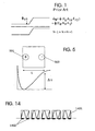
- FIG. 1 illustrates pn-junction barrier height as a function of band gap and Fermi level position.
- the Fermi level position corresponds to a dopant concentration.
- the addition or subtraction of one to a few extra dopant atoms or electrons to the system does not induce a significant change to the potential distribution.
- N B is the potential barrier height in a pn-junction
- Eg is semiconductor band gap
- E Fd and E Fa are Fermi levels in respectively acceptor-doped and donor-doped parts of semiconductor
- the present invention solves the above-described problem by providing materials and devices based on the creation of a supermolecular, semiconducting structure.
- This structure results from the controlled discrete distribution of, and arrangement of, single-impurity atoms or molecules within a host matrix, rather than on a stochastic distribution of dopants in a continuum or lattice environment.
- the general principle of operation is based on single charge effects, when considerable change in the potential in a system occurs due to addition, or modification, of a single charge.
- the invention provides a supermolecular structure made up of a host material with controlled impurities.
- the positions of the component atoms in the structure are fixed and controlled to impart predictable properties to the structure.
- the structure can be described by the empirical formula H A ⁇ X ia where H defines the host material, A is a number representing the number of host atoms in the structure, X defines the i th impurity, and a defines the quantity of the i th impurity.
- H defines the host material
- A is a number representing the number of host atoms in the structure
- X defines the i th impurity
- a defines the quantity of the i th impurity.
- the structure defined by this formula can be used to form a pn junction or a bipolar cell.
- a single-dopant pn junction is created by depositing a single donor atom so that it resides at a first side of a host structure, and depositing a single acceptor atom at a second, opposing side.
- the single donor and acceptor atoms are positioned so that a single dipole is created within the host structure.
- a pn junction device can be made from a cell as described here by building the structure on a substrate and attaching contact electrodes.
- the invention also facilitates creation of a single-dopant bipolar cell.
- a pair of atoms both either donor or acceptor atoms, resides at opposing sides of the host structure.
- a single atom is placed between the atoms of the pair. If the atoms in the pair are donors, the single atom is an acceptor. If the pair of atoms are acceptors, the single atom is a donor.
- the atoms are all positioned so that two asymmetrical potential wells, separated by a barrier, are formed within the semiconductor.
- the bipolar cell can be made into a stand-alone device by adding an insulating substrate and contact electrodes. This device can either function as a bistable device or an oscillator, depending on operating temperature, as will be discussed later.
- the present invention also can be used to create an oscillator array from a plurality of electrostatically coupled bipolar cells.
- This array can be used to make a semiconductor oscillator since the array provides a means of generating coherent oscillations that will result if the array is maintained at a temperature equal to or greater than a threshold temperature.
- An oscillator device is made from the array built on an insulating substrate. Contact electrodes are connected to the array as a means of connecting the device to external circuitry, and a thermal energy supply system is included to maintain the proper operating temperature of the array.
- Oscillator arrays and/or oscillator devices as described above can be used to make energy converters, seemingly self-powered electrical devices, wireless interconnects, and a myriad of other devices.
- Single-dopant cells according to the invention may be fabricated either horizontally or vertically.
- a single, three-atom set of dopants is placed on a semiconductor substrate.
- An epitaxial film of the semiconductor is grown over the three-atom set, and at least one, but usually several, insulating monolayers are passivated.
- Placing several three-atom sets of dopant atoms onto the substrate in the first step can make a plurality of horizontal cells.
- a pattern, which defines the shape of the cells, is produced at the surface of the epitaxial film.
- the three-atom set is formed vertically by placing a first atom of a first type on the substrate, growing a first epitaxial layer, placing a single atom of a second type on the first epitaxial layer and growing another epitaxial layer, and so on.
- the cell is again passivated at the end of the process.
- a plurality of vertical cells is fabricated by placing multiple first atoms of the first type, multiple single atoms of the second type, and multiple second atoms of the first type to form multiple, vertical three-atom sets.
- patterns defining the shapes of the cells are produced at the top epitaxial layer.
- FIG. 2 illustrates a hierarchy that summarizes the design flow that contributes to the correlation between microscopic structural parameters and macroscopic properties according to the invention.
- the structures of the invention exhibit unique properties due to either the single-charge effect, e.g. the large change in potential distribution in the system due to the addition, the removal, or displacement of a single charge; or the host effect, e.g. the influence of the local environment, including, but not limited to, factors such as materials selection, ambient temperature, etc. In many cases the structures take advantage of both of these effects.
- the host effect operates on potential surfaces and barriers near the dopants and donor-acceptor systems. These barriers can be designed to be symmetrical or asymmetrical, depending on device and system requirements. The host effect in turn affects kinetics mechanism(s) and trajectory of charge transfer.
- a single-dopant pn junction is created by depositing a donor and an acceptor atom at precise locations on the surface of or within a solid host matrix or lattice.
- This host structure, H may embody a variety of shapes and textures.
- the host structure, H, and the active cell can be thought of as a supermolecular structure. To aid understanding, this system can be conceptualized like other complex quasi-macromolecular structures, such as proteins or chromosomes.
- H is the host matrix or lattice element, where the subscript corresponds to the number of host elements in the chain connecting the terminus elements in the solid structure.
- X a is a dopant atom embedded in a local environment, such that the dopant can either be an electron acceptor or an electron donor.
- Y b is a dopant atom, that complements X a , embedded in a local environment, such that the dopant, Y b , can either be an electron acceptor or an electron donor.
- the empirical formula for such a supermolecular pn-junction type structure would be, H x D 1 A 1 , such that, X equals the total number of host atoms in the structure, D and A equals the two complementary dopant atoms.
- the positions of, and distances between dopants are accurately and precisely controlled.
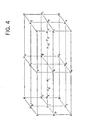
- a specific single dopant pn-junction such as a phosphorus atom, P a , and a boron atom, B b , attached to opposite sides of a silicon cube, as schematically shown in FIG. 6 .
- Such attachments can be made, for example, using proximity probe technology.
- This represents an ultimate pn-junction consisting of 1 donor and 1 acceptor atom.
- the macroscopic analogues of this system are conventional pn-junction devices and compensated semiconductors, as discussed in relationship to FIG. 1 .
- charge transfer has occurred and both dopants are ionized.
- the donor and the acceptor create a unique dipole within this structure.
- the barrier height of such an ultimate pn-junction is determined primarily by the charge separation d, which in this case is close to the cube linear dimension, L.
- the host environment provides a medium that also will effect the charge transfer and properties of the dopants and dipole. The addition of an extra charge will completely change the potential of the system.
- a single charge pn-junction is embedded in a cube of silicon, with dimension of 100 atoms on a side.
- a general empirical formula for this specific family of systems would be Si ⁇ 999998 P 1 B 1 or Si- 999998 D 1 A 1 for the general case of donors, D, and acceptors, A. This empirical formula does not completely define the structure, as it does not provide any information about the precise locations of the dopants within this cell.
- the example discussed above represents one class of generally shaped features that may be considered to be a rectangular cubic, H cubic .
- the cubic has a single donor atom positioned such that it resides in the center of one side of a host structure, mass, or cell, of semiconductor material, H cubic , and a single acceptor atom at a second, opposing side, at a specified distance from the donor atom. This distance may be defined by counting atoms in the supporting lattice or by other means.
- the single donor and acceptor atoms are positioned so that a single dipole is created within the host structure, H cubic .
- a pn junction device can be made from a cell as described here by building the mass, H, on a substrate and attaching contact electrodes.
- the properties of this device will be controlled by several factors, such as: the identity of dopants; the distance between and position of dopants; the composition and structure of the host matrix or lattice; the composition and structure of the local environment around the dopant atoms; the composition and structure of the environment around the host structure; and the nature of the interface with the outside world - electron or wireless interconnects, etc.
- the properties are also controlled by whether the dopant is embedded in the host molecule or a substituant is attached and/or placed in close proximity to the dopant.
- bipolar structure a pair of atoms, both either donor or acceptor atoms, reside at or are buried within opposing sides of the host structure. A single atom is placed between the atoms of the pair. If the atoms in the pair are donors, the single central atom is an acceptor. If the atoms in the pair are acceptors, the single atom between them is a donor. The atoms are all positioned so that two asymmetrical potential wells, separated by a barrier, are formed within the semiconductor.
- the bipolar cell can be made into a stand-alone device by adding an insulating substrate and contact electrodes. This device either can function as a bistable device or an oscillator, depending on operating temperature, as will be discussed later.
- the host structure, H, and active cell can again be thought of as a supermolecular structure. To aid understanding, this system can be conceptualized like other complex quasi-macromolecular structures, such as proteins or chromosomes.
- H the host matrix or lattice element
- X a is a dopant atom embedded in a local environment, such that the dopant can either be an electron acceptor or an electron donor.
- R a modifying substituant
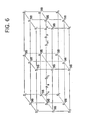
- FIG. 8 The specific case of a silicon cube, with dimensions of 100 atoms per side, containing two phosphorous atoms, P b , as donors and one boron atom, B c , as an acceptor, is shown in FIG. 8 .
- a general empirical formula for this specific family of systems would be Si ⁇ 999997 P 2 B 1 or Si- 999997 D 2 A 1 , for the general case of donors, D, and acceptors, A. This empirical formula does not completely define the structure, as it does not provide any information about the precise locations and positioning of the dopants within this cell.
- the SDBC forms two asymmetrical potential wells separated by a barrier.
- the potential of the cell is determined by two positive fixed charges, from donors 902, one negative fixed charge from acceptor 901, and one movable negative charge.
- the acceptor does not bind the second electron.
- the movable electron can be either in the well 1 or the well 2.
- Curves 904 and 905 illustrate the barrier height dependence. As the electron moves from well 1 into well 2, the potential distribution switches from 905 to 904 as shown in FIG. 9 .
- the cell could be built from two acceptors and one donor. The properties and behavior of this system depends on the potential distributions shown in curve 1301 of Figure 13 .
- the SDBC will exhibit two general modes of operation, depending upon the ambient temperature:
- the oscillation period, frequency, and power in the second case are, respectively: ⁇ ⁇ 1 / e ⁇ 2 ⁇ ⁇ 0 ⁇ ⁇ m e ⁇ L 3 1 / 2 f ⁇ 1 / ⁇ P ⁇ e ⁇ V 1 / ⁇ ( ⁇ is oscillation period, f is oscillation frequency, P is power of oscillations, e - is elementary charge, m e is electron mass, L is size of SDBC, ⁇ 0 is permittivity in vacuum, and ⁇ is the dielectric constant of the semiconductor.)
- FIG. 10 illustrates threshold temperature and other parameters as a function of cell size, L.
- T th threshold temperature
- oscillations occur spontaneously.
- heat is removed from the system.
- energy is converted from thermal energy to electromagnetic radiation. Maintaining these oscillations requires a permanent source of heat to power the system.
- the inverse process of converting electromagnet radiation into thermal energy can also be realized.
- Parameters of the oscillator as function of the cell size L are shown in FIG. 11 .
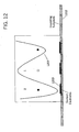
- FIG. 12 illustrates a stand-alone bipolar device according to the invention.
- the device includes an insulating substrate 1202 and contact electrodes 1203.
- Potential curve 1201 illustrates the potential wells of the two states of the device which cause bistable or oscillatory behavior.
- Fig. 13 illustrates an extension of the two-state device to a three-state device, where the potential distribution, 1301, comprehends three potential wells.
- the depths of the potential wells ⁇ V 1 , ⁇ V 2 , and ⁇ V 3 are functions of the local atomic level 'chemical' environment about each dopant atom. This device also will exhibit oscillatory behavior by tuning the potential threshold about each dopant atom.
- An SDBC can be fabricated either horizontally or vertically, relative to an initial substrate.
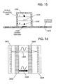
- the vertical structure of FIG. 15 can be fabricated by controlled layer-by-layer growth on an insulating substrate 1503, for example with molecular beam epitaxy (MBE) technology.
- MBE molecular beam epitaxy
- Such a structure is more feasible from the view of both fabrication and operation than horizontal structures.
- the dopants, 1501 and 1502 are completely embedded in the matrix and the surface is passivated, resulting in the passivation layer shown.
- Contact electrodes as shown at 1504 complete the device.
- the vertical structure allows for only one contact to the bottom electrode as compared to the horizontal structure. Also, the vertical structure is not suitable for long coherent oscillator arrays, as discussed below. However, short vertical arrays can be made over a distance of a few microns.
- n-p-n and p-n-p structures have quite different potential distribution. Both n-p-n and p-n-p structures allow for delocalized charges.
- the "flip-flop" transitions for the p-n-p system may require a two step mechanism. However, the n-p-n system switches via a more concerted process. In the latter case, the system will tend to exist in one of the following states: n + - p - - n 0 or n 0 - p - - n + .
- One state can flow directly into the other by a simple one step shift of the electrons associated with p - and n 0 towards the n + species.
- the p - n - p system can exist in following three distinct states: a) p 0 - n + - p - , b) p 0 - n 0 - p 0 , and c) p - - n + - p 0 .
- the transformation from state "a” to state "c” requires a two step mechanism that passes the intermediate state "b", as the movement of a single electron is responsible for effecting each of these discrete states.
- the properties of the p - n - p system can be tuned by controlling the local atomic environment and structure about the central "n" moiety. Shown below is one example that facilitates tuning or attenuation of the oscillator.
- Z represents the moiety that tunes the environment and potential about Y.
- Other devices, with unique properties, can be made by precisely positioning additional individual dopant atoms in close proximity to the other dopants. In this way, an integrated circuit based on the precise arrangement of atoms can be designed
- a linear array of single dopant bipolar cells, as shown in FIG. 14 will experience coherent oscillations.
- Phase oscillations spontaneously induced in individual cells, 1401 are random at first but eventually transform to in-phase (coherent) oscillations due to electrostatic coupling between the cells.
- Parameters of the oscillator array can be determined from the table of FIG. 11 .
- This array can be used to make a semiconductor oscillator since coherent oscillations will result if the array is maintained at a temperature equal to or greater than the threshold temperature.
- An oscillator device is made from the array built on an insulating substrate.
- Contact electrodes 1402 are connected to the array as a means of connecting the device to external circuitry and a thermal or other energy supply system is included to maintain the proper-operating temperature of the array.
- the electrodes may operate via electronic, charge coupled, or photonic means. Another function of the contact electrodes is to control the emergence of oscillations. If positive bias is applied to contact electrodes, the electrons will be 'frozen' in the cells. Thus, the transition from bistable to oscillating cell at a given temperature can be controlled by external bias.
- FIG. 16 illustrates an RF interconnect using single charge oscillator arrays.
- the transmitter (1601, 1602), and receiver (1603, 1604) are SCOA's of identical cell size.
- the oscillations in the transmitter SCOA selectively induce oscillations in the receiver SCOA.
- the selectivity of transmission lines (1605 and 1606) is determined by the size-specificity of oscillation.
- the oscillations in the transmitter SCOA can be suspended or released by applying control commands to underlying contacts (1402 in Fig. 14 ).
- Oscillator arrays that use the invention can also be used to make self-powered devices.
- a specific feature of the proposed oscillator array is that, under the right conditions, its operation does not require an external supply of electric energy. Instead, oscillations occur spontaneously at a certain temperature, as defined by the structural specifications of the system.
- the oscillator array is powered by thermal energy and will continue to function, as long as a certain minimum temperature is maintained. Thermodynamically, this situation resembles hurricane formation (coherent oscillation/perturbation) over an ocean surface when the ocean temperature is increased by only few degrees above the normal temperature. For example, a two to three degree increase in ocean temperature is enough to convert the thermal energy of the ocean into the disruptive mechanical energy of the hurricane. As can be seen from the table in FIG.
- the oscillator array can be used for transmitting signals. Also, this device can convert microwave power along the circuit into electric DC power, by a simple rectification process. Thus, in addition to signal T-R pairs in the interconnect above, it is possible to make power T-R pairs.
- the power varies with array length. In principle, this approach allows for the elimination of an external electric power supply, at least for low power applications, provided any suitable source of heat provides power to the circuit, as specified in FIG. 11 .
- This self-power capability can be used in electronic circuits as well as in numerous other applications, such as, but not limited to, "smart skins".
- the threshold energy is so low that it could be powered by being in contact with or in close proximity to a living body.
- the energy of this ambient environment is sufficient to power this system.
- the capability also allows the arrays to be used as energy converters. Macroscopic single charge oscillator arrays, SCOA, can be used for general energetic purposes.
- a device could be designed with a threshold so low that it could be powered by the temperature of the ambient environment.
- the size and shape of individual host cell structures, H are defined by submicron and nanoscale patterning.
- Techniques for fabricating patterned cells include, but are not limited to: lithography, both conventional and so-called "next generation lithography” (NGL); maskless patterning; imprint or 'step and flash' patterning or self assembly; and thin film or interface deposition by chemical vapor deposition (CVD), molecular beam epitaxy (MBE) or atomic layer epitaxy (ALE).
- CVD chemical vapor deposition
- MBE molecular beam epitaxy
- ALE atomic layer epitaxy
- the precise positional assembly of individual dopant atoms can be achieved by proximity probe manipulation of individual atoms at low temperatures.
- the fixing of the atomic positions of dopants and suppression of their movement can be accomplished by topography or surface driven segregation of dopants and/or surface passivation, electron-irradiation modification of materials properties, or the use of porous materials with controlled shape and distribution of pores, such as porous polymers, porous diamond, and porous calcium fluoride.
- MBE molecular beam epitaxy
- Maskless patterning methods such as probe lithography, are used to position individual dopant atoms at precise locations on the silicon surface at low temperatures. MBE continues to build up the thickness of the silicon lattice and embed the dopants at precise locations within this structure.
- Holographic patterning methods can be used to define regions to etch, for isolating individual structures. Alternatively, the final etch, a subtractive process, can be eliminated if an MBE resistant region is defined lithographically prior to the first step, listed above.
- dopant atoms can be arranged colinearly, in a vertical manner, by alternating the MBE and maskless patterning steps described above, until the three dopant atoms are positioned.
- Final MBE and holographic patterning complete the fabrication of this vertical cell.
- a method of making an atomic chain circuit by placing atoms at predetermined locations is described in U.S. Patent No. 5,981,316, issued November 9, 1999 , which is incorporated herein by reference. That method is based on recent progress in atom manipulation technology that allows a fabricator to move atoms one by one and arrange them as desired using a proximity probe manipulation (PPM) technique.
- PPM proximity probe manipulation
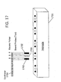
- FIG. 17 SDBC's are made by placing three dopant atoms in a line with fixed separations in between.
- a cantilever 1704 supports a 3-probe PPM system.
- Bound probes 1702 place one type of atom, and bound probe 1703 places another.
- This system enables "stamping" arrays of identical sets of 3 dopants at a substrate, 1701. Carbon nanotube-based probes are preferable for this sort of application. Addressable multiprobe arrays further extend this fabrication concept towards high-yield production.
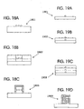
- a horizontal, silicon-based SDBC is fabricated with the system in FIG. 17 as shown in FIG. 18 according to the following method.
- An epitaxial film of Si is grown by low temperature MBE (LT MBE) or low temperature CVD (LT CVD). The film thickness is half of the cell size.
- the resulting structure is shown at 1802 in FIG. 18B .
- Patterns e.g. squares
- the surface of the cell is passivated by few monolayers of SiO 2 , hydrogen, or CaF 2 , as shown by cross-hatching.
- the structure 1803, shown in FIG. 18C results.
- FIG. 19 illustrates the fabrication of a vertical, silicon-based SDBC.
- one or two probes place the atoms, as they are not placed in sets of three.
- a first dopant atom is placed at the Si substrate as shown at 1901 in FIG. 19A .
- An epitaxial film of Si is then grown by LT MBE, the epitaxial film having a thickness of one third of the cell size.
- a second dopant is place atop the structure as shown at 1902 in FIG. 19B .
- the second dopant atom is placed at exactly the same horizontal spatial coordinate as the first dopant atom.
- Another epitaxial Si film is grown over the second dopant atom.
- a third dopant atom is placed on the structure.
- the horizontal spatial coordinate for this atom is the same as for the first two atoms.
- Another epitaxial film is grown resulting in structure 1903 shown in FIG. 19C . All epitaxial films are equal to one third the desired cell size.
- patterns e.g. squares
- the surface of the cell is again passivated by few monolayers of SiO 2 hydrogen, or CaF 2 , as shown by cross-hatching, and the structure 1904 as shown in FIG. 19D results.
Landscapes
- Bipolar Transistors (AREA)
- Semiconductor Memories (AREA)
- Recrystallisation Techniques (AREA)
- Stabilization Of Oscillater, Synchronisation, Frequency Synthesizers (AREA)
Applications Claiming Priority (2)
| Application Number | Priority Date | Filing Date | Title |
|---|---|---|---|
| US09/510,802 US6664559B1 (en) | 2000-02-23 | 2000-02-23 | Supermolecular structures and devices made from same |
| EP01911082A EP1258041A2 (fr) | 2000-02-23 | 2001-02-22 | Structures supermoleculaires et dispositifs fabriques a partir desdites structures |
Related Parent Applications (2)
| Application Number | Title | Priority Date | Filing Date |
|---|---|---|---|
| EP01911082.4 Division | 2001-02-22 | ||
| EP01911082A Division EP1258041A2 (fr) | 2000-02-23 | 2001-02-22 | Structures supermoleculaires et dispositifs fabriques a partir desdites structures |
Publications (3)
| Publication Number | Publication Date |
|---|---|
| EP2009699A2 true EP2009699A2 (fr) | 2008-12-31 |
| EP2009699A3 EP2009699A3 (fr) | 2010-03-31 |
| EP2009699B1 EP2009699B1 (fr) | 2013-04-24 |
Family
ID=24032251
Family Applications (2)
| Application Number | Title | Priority Date | Filing Date |
|---|---|---|---|
| EP01911082A Ceased EP1258041A2 (fr) | 2000-02-23 | 2001-02-22 | Structures supermoleculaires et dispositifs fabriques a partir desdites structures |
| EP08017802.3A Expired - Lifetime EP2009699B1 (fr) | 2000-02-23 | 2001-02-22 | Structures supramoléculaires et dispositifs les comprenant |
Family Applications Before (1)
| Application Number | Title | Priority Date | Filing Date |
|---|---|---|---|
| EP01911082A Ceased EP1258041A2 (fr) | 2000-02-23 | 2001-02-22 | Structures supermoleculaires et dispositifs fabriques a partir desdites structures |
Country Status (4)
| Country | Link |
|---|---|
| US (2) | US6664559B1 (fr) |
| EP (2) | EP1258041A2 (fr) |
| TW (1) | TWI230406B (fr) |
| WO (1) | WO2001063674A2 (fr) |
Families Citing this family (4)
| Publication number | Priority date | Publication date | Assignee | Title |
|---|---|---|---|---|
| US7015546B2 (en) * | 2000-02-23 | 2006-03-21 | Semiconductor Research Corporation | Deterministically doped field-effect devices and methods of making same |
| GB0116943D0 (en) * | 2001-07-11 | 2001-09-05 | Isis Innovation | Information register |
| WO2013074967A1 (fr) | 2011-11-17 | 2013-05-23 | Gentherm Incorporated | Dispositifs thermoélectriques ayant des matières d'interface et procédés de fabrication de ceux-ci |
| US11223004B2 (en) | 2018-07-30 | 2022-01-11 | Gentherm Incorporated | Thermoelectric device having a polymeric coating |
Citations (1)
| Publication number | Priority date | Publication date | Assignee | Title |
|---|---|---|---|---|
| US5981316A (en) | 1994-11-08 | 1999-11-09 | The Board Of Trustees Of The Leland Stanford Junior University | Method of fabrication of atomic chain circuit network |
Family Cites Families (6)
| Publication number | Priority date | Publication date | Assignee | Title |
|---|---|---|---|---|
| US6525336B1 (en) * | 1991-12-24 | 2003-02-25 | Hitachi, Ltd. | Superfine electronic device and method for making same |
| DE69228524T2 (de) * | 1991-12-24 | 1999-10-28 | Hitachi, Ltd. | Atomare Vorrichtungen und atomare logische Schaltungen |
| JP2723099B2 (ja) | 1995-12-28 | 1998-03-09 | 日本電気株式会社 | クラスレート化合物およびその製造方法 |
| JP4103968B2 (ja) * | 1996-09-18 | 2008-06-18 | 株式会社半導体エネルギー研究所 | 絶縁ゲイト型半導体装置 |
| DE19881312D2 (de) | 1997-09-09 | 2001-01-18 | Schmitt Klaus | P-dotiertes Silizium-Makromolekül mit mehrflächiger Struktur, Verfahren zu seiner Herstellung und Vorrichtung zur Durchführung des Verfahrens sowie basierend auf dem Silizium-Makromolekül aufgebauter Transistor |
| US6068698A (en) | 1997-10-02 | 2000-05-30 | Schmidt; Christian | P-type silicon macromolecule used in a transistor and process for manufacture of the macromolecule |
-
2000
- 2000-02-23 US US09/510,802 patent/US6664559B1/en not_active Expired - Fee Related
-
2001
- 2001-02-22 WO PCT/US2001/005595 patent/WO2001063674A2/fr not_active Ceased
- 2001-02-22 EP EP01911082A patent/EP1258041A2/fr not_active Ceased
- 2001-02-22 EP EP08017802.3A patent/EP2009699B1/fr not_active Expired - Lifetime
- 2001-02-23 TW TW090104191A patent/TWI230406B/zh not_active IP Right Cessation
-
2003
- 2003-10-14 US US10/685,041 patent/US6897470B2/en not_active Expired - Fee Related
Patent Citations (1)
| Publication number | Priority date | Publication date | Assignee | Title |
|---|---|---|---|---|
| US5981316A (en) | 1994-11-08 | 1999-11-09 | The Board Of Trustees Of The Leland Stanford Junior University | Method of fabrication of atomic chain circuit network |
Non-Patent Citations (1)
| Title |
|---|
| S. M. SZE: "Physics of Semiconductor Devices", 1981, JOHNE WHILEY & SONS, INC |
Also Published As
| Publication number | Publication date |
|---|---|
| EP1258041A2 (fr) | 2002-11-20 |
| US6664559B1 (en) | 2003-12-16 |
| EP2009699B1 (fr) | 2013-04-24 |
| EP2009699A3 (fr) | 2010-03-31 |
| WO2001063674A3 (fr) | 2002-05-30 |
| US6897470B2 (en) | 2005-05-24 |
| TWI230406B (en) | 2005-04-01 |
| US20050062036A1 (en) | 2005-03-24 |
| WO2001063674A2 (fr) | 2001-08-30 |
Similar Documents
| Publication | Publication Date | Title |
|---|---|---|
| US8641912B2 (en) | Method for fabricating monolithic two-dimensional nanostructures | |
| KR100272702B1 (ko) | 터널 효과 장치 및 그 제조 방법 | |
| JP4499418B2 (ja) | 分子電子素子を製造する方法 | |
| US7087920B1 (en) | Nanowire, circuit incorporating nanowire, and methods of selecting conductance of the nanowire and configuring the circuit | |
| US7015546B2 (en) | Deterministically doped field-effect devices and methods of making same | |
| KR101008294B1 (ko) | 나노구조체 및 나노와이어의 제조 방법 및 그로부터 제조되는 디바이스 | |
| EP3542402A1 (fr) | Matériaux bidimensionnels intégrés à des couches multiferroïques | |
| Sumant et al. | MEMS/NEMS based on mono-, nano-, and ultrananocrystalline diamond films | |
| US20160056304A1 (en) | Nanowire nanoelectromechanical field-effect transistors | |
| US20100060383A1 (en) | Carbon Nanotube Resonators | |
| EP2009699B1 (fr) | Structures supramoléculaires et dispositifs les comprenant | |
| Chen et al. | A double quantum dot defined by top gates in a single crystalline InSb nanosheet | |
| US7214571B2 (en) | Electromechanical electron transfer devices | |
| Narayanan et al. | Manufacturing pathway and associated challenges for nanoscale computational systems | |
| WO2008147432A2 (fr) | Procédé d'assemblage de nanostructures unidimensionnelles | |
| Zhang et al. | Electromagnetic Field‐Responsive and Accurate Control of Bending in VO2 Based Micro‐Pillar Array | |
| Kamins et al. | Trends in nanotechnology: Self-assembly and defect tolerance | |
| Cerofolini et al. | Terascale integration via a redesign of the crossbar based on a vertical arrangement of poly-Si nanowires | |
| Obukhov | 14. SOME ASPECTS OF NANOELECTRONICS DEVELOPMENT IN RUSSIA | |
| Karmous et al. | Recent developments in Ge dots grown on pit‐patterned surfaces | |
| Saxena et al. | Novel nanoelectronic materials and devices: For future technology node | |
| Edgar et al. | Recent developments and current challenges in interfacing and integrating 1D semiconductor nanowires in devices and circuits | |
| Zhao et al. | A novel paradigm for the fabrication of highly uniform nanowire arrays using residual stress-induced patterning | |
| CN101326535A (zh) | 一维纳米结构螺旋感应器 | |
| Kamins et al. | Self-Assembled Semiconductor Nanowires on Silicon and Insulating Substrates: Experimental Behavior |
Legal Events
| Date | Code | Title | Description |
|---|---|---|---|
| PUAI | Public reference made under article 153(3) epc to a published international application that has entered the european phase |
Free format text: ORIGINAL CODE: 0009012 |
|
| AC | Divisional application: reference to earlier application |
Ref document number: 1258041 Country of ref document: EP Kind code of ref document: P |
|
| AK | Designated contracting states |
Kind code of ref document: A2 Designated state(s): AT BE CH CY DE DK ES FI FR GB GR IE IT LI LU MC NL PT SE TR |
|
| PUAL | Search report despatched |
Free format text: ORIGINAL CODE: 0009013 |
|
| AK | Designated contracting states |
Kind code of ref document: A3 Designated state(s): AT BE CH CY DE DK ES FI FR GB GR IE IT LI LU MC NL PT SE TR |
|
| 17P | Request for examination filed |
Effective date: 20100930 |
|
| AKX | Designation fees paid |
Designated state(s): AT BE CH CY DE DK ES FI FR GB GR IE IT LI LU MC NL PT SE TR |
|
| 17Q | First examination report despatched |
Effective date: 20101215 |
|
| GRAP | Despatch of communication of intention to grant a patent |
Free format text: ORIGINAL CODE: EPIDOSNIGR1 |
|
| GRAS | Grant fee paid |
Free format text: ORIGINAL CODE: EPIDOSNIGR3 |
|
| GRAA | (expected) grant |
Free format text: ORIGINAL CODE: 0009210 |
|
| AC | Divisional application: reference to earlier application |
Ref document number: 1258041 Country of ref document: EP Kind code of ref document: P |
|
| AK | Designated contracting states |
Kind code of ref document: B1 Designated state(s): AT BE CH CY DE DK ES FI FR GB GR IE IT LI LU MC NL PT SE TR |
|
| REG | Reference to a national code |
Ref country code: GB Ref legal event code: FG4D |
|
| REG | Reference to a national code |
Ref country code: CH Ref legal event code: EP |
|
| REG | Reference to a national code |
Ref country code: AT Ref legal event code: REF Ref document number: 609072 Country of ref document: AT Kind code of ref document: T Effective date: 20130515 |
|
| REG | Reference to a national code |
Ref country code: IE Ref legal event code: FG4D |
|
| REG | Reference to a national code |
Ref country code: DE Ref legal event code: R096 Ref document number: 60147934 Country of ref document: DE Effective date: 20130620 |
|
| REG | Reference to a national code |
Ref country code: AT Ref legal event code: MK05 Ref document number: 609072 Country of ref document: AT Kind code of ref document: T Effective date: 20130424 |
|
| REG | Reference to a national code |
Ref country code: NL Ref legal event code: VDEP Effective date: 20130424 |
|
| PG25 | Lapsed in a contracting state [announced via postgrant information from national office to epo] |
Ref country code: GR Free format text: LAPSE BECAUSE OF FAILURE TO SUBMIT A TRANSLATION OF THE DESCRIPTION OR TO PAY THE FEE WITHIN THE PRESCRIBED TIME-LIMIT Effective date: 20130725 Ref country code: PT Free format text: LAPSE BECAUSE OF FAILURE TO SUBMIT A TRANSLATION OF THE DESCRIPTION OR TO PAY THE FEE WITHIN THE PRESCRIBED TIME-LIMIT Effective date: 20130826 Ref country code: AT Free format text: LAPSE BECAUSE OF FAILURE TO SUBMIT A TRANSLATION OF THE DESCRIPTION OR TO PAY THE FEE WITHIN THE PRESCRIBED TIME-LIMIT Effective date: 20130424 Ref country code: ES Free format text: LAPSE BECAUSE OF FAILURE TO SUBMIT A TRANSLATION OF THE DESCRIPTION OR TO PAY THE FEE WITHIN THE PRESCRIBED TIME-LIMIT Effective date: 20130804 Ref country code: FI Free format text: LAPSE BECAUSE OF FAILURE TO SUBMIT A TRANSLATION OF THE DESCRIPTION OR TO PAY THE FEE WITHIN THE PRESCRIBED TIME-LIMIT Effective date: 20130424 Ref country code: BE Free format text: LAPSE BECAUSE OF FAILURE TO SUBMIT A TRANSLATION OF THE DESCRIPTION OR TO PAY THE FEE WITHIN THE PRESCRIBED TIME-LIMIT Effective date: 20130424 Ref country code: SE Free format text: LAPSE BECAUSE OF FAILURE TO SUBMIT A TRANSLATION OF THE DESCRIPTION OR TO PAY THE FEE WITHIN THE PRESCRIBED TIME-LIMIT Effective date: 20130424 |
|
| PG25 | Lapsed in a contracting state [announced via postgrant information from national office to epo] |
Ref country code: CY Free format text: LAPSE BECAUSE OF FAILURE TO SUBMIT A TRANSLATION OF THE DESCRIPTION OR TO PAY THE FEE WITHIN THE PRESCRIBED TIME-LIMIT Effective date: 20130424 |
|
| PG25 | Lapsed in a contracting state [announced via postgrant information from national office to epo] |
Ref country code: DK Free format text: LAPSE BECAUSE OF FAILURE TO SUBMIT A TRANSLATION OF THE DESCRIPTION OR TO PAY THE FEE WITHIN THE PRESCRIBED TIME-LIMIT Effective date: 20130424 |
|
| PG25 | Lapsed in a contracting state [announced via postgrant information from national office to epo] |
Ref country code: IT Free format text: LAPSE BECAUSE OF FAILURE TO SUBMIT A TRANSLATION OF THE DESCRIPTION OR TO PAY THE FEE WITHIN THE PRESCRIBED TIME-LIMIT Effective date: 20130424 Ref country code: NL Free format text: LAPSE BECAUSE OF FAILURE TO SUBMIT A TRANSLATION OF THE DESCRIPTION OR TO PAY THE FEE WITHIN THE PRESCRIBED TIME-LIMIT Effective date: 20130424 |
|
| PLBE | No opposition filed within time limit |
Free format text: ORIGINAL CODE: 0009261 |
|
| STAA | Information on the status of an ep patent application or granted ep patent |
Free format text: STATUS: NO OPPOSITION FILED WITHIN TIME LIMIT |
|
| 26N | No opposition filed |
Effective date: 20140127 |
|
| REG | Reference to a national code |
Ref country code: DE Ref legal event code: R097 Ref document number: 60147934 Country of ref document: DE Effective date: 20140127 |
|
| REG | Reference to a national code |
Ref country code: DE Ref legal event code: R119 Ref document number: 60147934 Country of ref document: DE |
|
| PG25 | Lapsed in a contracting state [announced via postgrant information from national office to epo] |
Ref country code: LU Free format text: LAPSE BECAUSE OF FAILURE TO SUBMIT A TRANSLATION OF THE DESCRIPTION OR TO PAY THE FEE WITHIN THE PRESCRIBED TIME-LIMIT Effective date: 20140222 Ref country code: MC Free format text: LAPSE BECAUSE OF FAILURE TO SUBMIT A TRANSLATION OF THE DESCRIPTION OR TO PAY THE FEE WITHIN THE PRESCRIBED TIME-LIMIT Effective date: 20130424 |
|
| REG | Reference to a national code |
Ref country code: CH Ref legal event code: PL |
|
| GBPC | Gb: european patent ceased through non-payment of renewal fee |
Effective date: 20140222 |
|
| PG25 | Lapsed in a contracting state [announced via postgrant information from national office to epo] |
Ref country code: LI Free format text: LAPSE BECAUSE OF NON-PAYMENT OF DUE FEES Effective date: 20140228 Ref country code: CH Free format text: LAPSE BECAUSE OF NON-PAYMENT OF DUE FEES Effective date: 20140228 |
|
| REG | Reference to a national code |
Ref country code: FR Ref legal event code: ST Effective date: 20141031 |
|
| REG | Reference to a national code |
Ref country code: DE Ref legal event code: R119 Ref document number: 60147934 Country of ref document: DE Effective date: 20140902 |
|
| REG | Reference to a national code |
Ref country code: IE Ref legal event code: MM4A |
|
| PG25 | Lapsed in a contracting state [announced via postgrant information from national office to epo] |
Ref country code: DE Free format text: LAPSE BECAUSE OF NON-PAYMENT OF DUE FEES Effective date: 20140902 Ref country code: IE Free format text: LAPSE BECAUSE OF NON-PAYMENT OF DUE FEES Effective date: 20140222 Ref country code: FR Free format text: LAPSE BECAUSE OF NON-PAYMENT OF DUE FEES Effective date: 20140228 Ref country code: GB Free format text: LAPSE BECAUSE OF NON-PAYMENT OF DUE FEES Effective date: 20140222 |
|
| PG25 | Lapsed in a contracting state [announced via postgrant information from national office to epo] |
Ref country code: TR Free format text: LAPSE BECAUSE OF FAILURE TO SUBMIT A TRANSLATION OF THE DESCRIPTION OR TO PAY THE FEE WITHIN THE PRESCRIBED TIME-LIMIT Effective date: 20130424 |