EP2009758A1 - Procédé et système de commande de modulation de circuit syntonique - Google Patents
Procédé et système de commande de modulation de circuit syntonique Download PDFInfo
- Publication number
- EP2009758A1 EP2009758A1 EP07710934A EP07710934A EP2009758A1 EP 2009758 A1 EP2009758 A1 EP 2009758A1 EP 07710934 A EP07710934 A EP 07710934A EP 07710934 A EP07710934 A EP 07710934A EP 2009758 A1 EP2009758 A1 EP 2009758A1
- Authority
- EP
- European Patent Office
- Prior art keywords
- voltage
- module
- vloop
- controlling
- loop circuit
- Prior art date
- Legal status (The legal status is an assumption and is not a legal conclusion. Google has not performed a legal analysis and makes no representation as to the accuracy of the status listed.)
- Withdrawn
Links
Images





Classifications
-
- H—ELECTRICITY
- H02—GENERATION; CONVERSION OR DISTRIBUTION OF ELECTRIC POWER
- H02M—APPARATUS FOR CONVERSION BETWEEN AC AND AC, BETWEEN AC AND DC, OR BETWEEN DC AND DC, AND FOR USE WITH MAINS OR SIMILAR POWER SUPPLY SYSTEMS; CONVERSION OF DC OR AC INPUT POWER INTO SURGE OUTPUT POWER; CONTROL OR REGULATION THEREOF
- H02M3/00—Conversion of DC power input into DC power output
- H02M3/22—Conversion of DC power input into DC power output with intermediate conversion into AC
- H02M3/24—Conversion of DC power input into DC power output with intermediate conversion into AC by static converters
- H02M3/28—Conversion of DC power input into DC power output with intermediate conversion into AC by static converters using discharge tubes with control electrode or semiconductor devices with control electrode to produce the intermediate AC
- H02M3/325—Conversion of DC power input into DC power output with intermediate conversion into AC by static converters using discharge tubes with control electrode or semiconductor devices with control electrode to produce the intermediate AC using devices of a triode or a transistor type requiring continuous application of a control signal
- H02M3/335—Conversion of DC power input into DC power output with intermediate conversion into AC by static converters using discharge tubes with control electrode or semiconductor devices with control electrode to produce the intermediate AC using devices of a triode or a transistor type requiring continuous application of a control signal using semiconductor devices only
- H02M3/33507—Conversion of DC power input into DC power output with intermediate conversion into AC by static converters using discharge tubes with control electrode or semiconductor devices with control electrode to produce the intermediate AC using devices of a triode or a transistor type requiring continuous application of a control signal using semiconductor devices only with automatic control of the output voltage or current, e.g. flyback converters
-
- Y—GENERAL TAGGING OF NEW TECHNOLOGICAL DEVELOPMENTS; GENERAL TAGGING OF CROSS-SECTIONAL TECHNOLOGIES SPANNING OVER SEVERAL SECTIONS OF THE IPC; TECHNICAL SUBJECTS COVERED BY FORMER USPC CROSS-REFERENCE ART COLLECTIONS [XRACs] AND DIGESTS
- Y02—TECHNOLOGIES OR APPLICATIONS FOR MITIGATION OR ADAPTATION AGAINST CLIMATE CHANGE
- Y02B—CLIMATE CHANGE MITIGATION TECHNOLOGIES RELATED TO BUILDINGS, e.g. HOUSING, HOUSE APPLIANCES OR RELATED END-USER APPLICATIONS
- Y02B70/00—Technologies for an efficient end-user side electric power management and consumption
- Y02B70/10—Technologies improving the efficiency by using switched-mode power supplies [SMPS], i.e. efficient power electronics conversion e.g. power factor correction or reduction of losses in power supplies or efficient standby modes
Definitions
- the present invention generally relates to electrical communication technique, and more particularly, to a modulation control method and system for a resonance circuit.
- required output voltage can be obtained by modulating operating frequency of a switch tube in the resonance circuit in a PFM (Pulse Frequency Modulation) mode.
- PFM Pulse Frequency Modulation
- resonant transformation technique is applied to series resonance DC/DC converter. Since resonant elements are in sinusoidal resonance state, voltage on the switch tube passes zero naturally, and zero voltage turn-on can be realized. At the same time, reverse recovery of output rectifier diodes can be eliminated, and loss of power supply can be reduced and efficiency can be improved. In such topologies, typically, output voltage can be stabilized by modulating operating frequency of a switch tube in a PFM mode.
- Lr is the value of resonant inductance
- f is the operating frequency of the switch tube
- Cr is the value of resonant capacitance
- Po is an output power
- simple variable frequency control will result in excessively high operating frequency and excessively wide regulating range, and will make it more difficult to design the magnetic elements, and lower the efficiency of the power supply as well. So, simple variable frequency control can not meet the requirement of a stable output voltage of a converter in light load and no load state.
- An object of the present invention is to provide a modulation control method and system for a resonance circuit of low cost and high efficiency, so as to solve the problem in the prior art that simple variable frequency control will result in excessively high operating frequency and excessively wide regulating range, and will make it more difficult to design the magnetic elements, and lower the efficiency of the power supply.
- a modulation control system for a resonance circuit of the present invention wherein a controlling chip of the resonance circuit is connected to an associated controlling means that provides voltage matching and resistance control to the controlling chip, the controlling means providing controlling parameters to the modulating controlling chip in accordance with an input voltage, the controlling chip modulating the resonance circuit accordingly.
- the controlling chip is a phase-shift pulse-width modulation controlling chip, a PWM generator and oscillator of which are connected to a voltage matching module and a resistance controlling module of the controlling means, respectively; the voltage matching module and the resistance controlling module providing the controlling parameters to the phase-shift pulse-width modulation controlling chip in accordance with the input voltage; the phase-shift pulse-width modulation controlling chip modulating the resonance circuit accordingly.
- Both the voltage matching module and the resistance controlling module use a loop circuit voltage Vloop as the input voltage
- the voltage matching module matches a phase-shift voltage interval corresponding to the loop circuit voltage Vloop with a voltage range in which the phase is shifted by the PWM generator of the phase-shift pulse-width modulation controlling chip;
- the resistance controlling module is connected between the loop circuit voltage Vloop and the oscillator of the phase-shift pulse-width modulation controlling chip, such that an equivalent resistance of the oscillator to the external is regulated accordingly as the loop circuit voltage Vloop changes.
- the voltage matching module comprises an operational amplifier U701, a first voltage dividing sub-module and a current limiting circuit, and wherein, a resistor R714 is connected between an inverting terminal of the operational amplifier U701 and ground, while a resistor R711 is connected between the inverting terminal of the operational amplifier U701 and an output terminal; a non-inverting terminal of the operational amplifier U701 is connected to a voltage dividing terminal of the first voltage dividing sub-module; the current limiting circuit is connected between an output terminal of the operational amplifier U701 and the PWM generator of the phase-shift pulse-width modulation controlling chip.
- the resistance controlling module comprises a second voltage dividing sub-module, a resistor R703 being connected between a voltage dividing terminal of the second voltage dividing sub-module and the oscillator of the phase-shift pulse-width modulation controlling chip.
- the controlling chip is a pulse-width modulation controlling chip; a COMP terminal and a RT terminal of which is connected to a voltage matching module and a resistance controlling module of the controlling means, respectively; the voltage matching module and the resistance controlling module provide the controlling parameters to the pulse-width modulation controlling chip in accordance with the input voltage, the pulse-width modulation controlling chip modulates the resonance circuit accordingly.
- Both the voltage matching module and the resistance controlling module use the loop circuit voltage Vloop as the input voltage
- the voltage matching module matches a width-modulated voltage interval corresponding to the loop circuit voltage Vloop with a voltage range in which the phase is width-modulated by the COMP terminal of the pulse-width modulation controlling chip;
- the resistance controlling module is connected between the loop circuit voltage Vloop and the RT terminal of the pulse-width modulation controlling chip such that an equivalent resistance of the RT terminal to the external is regulated accordingly as the loop circuit voltage Vloop changes.
- the voltage matching module comprises an operational amplifier U701, a first voltage dividing sub-module and a current limiting circuit, and wherein, a resistor R714 is connected between an inverting terminal of the operational amplifier U701 and ground, while a resistor R711 is connected between the inverting terminal of the operational amplifier U701 and an output terminal; a non-inverting terminal of the operational amplifier U701 is connected to a voltage dividing terminal of the first voltage dividing sub-module; the current limiting circuit is connected between the output terminal of the operational amplifier U701 and the COMP terminal of the pulse-width modulation controlling chip.
- the resistance controlling module comprises a second voltage dividing sub-module, wherein a resistor R703 is connected between a voltage dividing terminal of the second voltage dividing sub-module and the oscillator of the phase-shift pulse-width modulation controlling chip.
- the first voltage dividing sub-module comprises series resistors R712 and R713, and is connected between the loop circuit voltage and the ground.
- the second voltage dividing sub-module comprises series resistors R701 and R702, and is connected between the loop circuit voltage and the ground.
- the resistance controlling module further comprises a voltage-comparing sub-module, that generates a reference level Vref, and wherein a first diode D702 is connected between the reference level Vref and the input terminal of the second voltage-dividing sub-module 31, while a second diode D701 is connected between the loop circuit voltage Vloop and the input terminal of the second voltage-dividing sub-module 31, with cathodes of the first diode D702 and the second diode D701 being connected with the second voltage-dividing sub-module.
- a modulation control method for a resonance circuit wherein: a phase-shift pulse-width modulation controlling chip is used so as to realize controlling modes of frequency-modulation, width-modulation and combination thereof for the resonance circuit through a voltage matching module and a resistance controlling module.
- the method comprises the following steps:
- the method comprises the following steps:
- the maximum duty ratio is 50%.
- the first interval is a phase-shift voltage interval of the loop circuit voltage Vloop when the resonance circuit is in light load or no load state.
- the third interval is a phase-shift voltage interval of the loop circuit voltage Vloop when the resonance circuit is in a heavy load state.
- a modulation control method for a resonance circuit characterized in that a pulse-width modulation controlling chip is used so as to realize controlling modes of frequency-modulation, width-modulation and combination thereof for the resonance circuit through a voltage matching module and a resistance controlling module.
- the method comprises the following steps:
- the method comprises the following steps:
- the maximum duty ratio is 50%.
- the first interval is a width-modulated voltage interval of the loop circuit voltage Vloop when the resonance circuit is in light load or no load state.
- the third interval is a frequency-modulated voltage interval of the loop circuit voltage Vloop when the resonance circuit is in a heavy load state.
- the loop circuit voltage Vloop is an output voltage which is an output voltage of the resonance circuit Vo having passed through a sampling circuit and a regulator.
- a controlling chip of the resonance circuit is connected to associated controlling means for providing voltage matching and resistance control to the modulating controlling chip.
- the controlling means provides controlling parameters to the modulating controlling chip in accordance with an input voltage, and the controlling chip modulates the resonance circuit accordingly.
- the controlling chip may be width-modulated controlling chip or phase-shift pulse-width modulation controlling chip, in which a PWM generator and oscillator are connected to a voltage matching module and a resistance controlling module respectively.
- the voltage matching module and the resistance controlling module provide corresponding controlling parameters to the phase-shift pulse-width modulation controlling chip in accordance with the input voltage, and perform corresponding modulation.
- the voltage matching module and the resistance controlling module use the loop circuit voltage Vloop as input voltage.
- the loop circuit voltage Vloop operates in a first interval, in which Vloop is relatively small, and thus suggests that the converter is in light load or no load state, it causes the resistance controlling module to act on the phase-shift pulse-width modulation controlling chip to generate frequency-modulating control.
- the loop circuit voltage Vloop causes the voltage matching module to act on the phase-shift pulse-width modulation controlling chip to generate width-modulating control.
- an operational amplifier U701 and simple separate elements are used in the voltage matching module, while a resistor or combination of resistors are connected to the RT terminal in the resistance controlling module.
- the present invention is advantageous in its simple structure and low cost. Although same modulation performance is obtained, the present invention reduces the difficulty of designing magnetic elements and improves power efficiency.
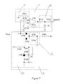
- the present invention includes a phase-shift pulse-width modulation controlling chip 1.
- EAOUT terminal of a PWM generator and RT terminal of an oscillator of the phase-shift pulse-width modulation controlling chip are connected to a voltage matching module 2 and a resistance controlling module 3 respectively.
- the voltage matching module 2 and the resistance controlling module 3 provide corresponding controlling parameters to the phase-shift pulse-width modulation controlling chip 1 in accordance with the input voltage (i.e., the loop circuit voltage Vloop).
- the phase-shift pulse-width modulation controlling chip 1 modulates the resonance circuit accordingly.
- S1, S2, S4 and S3 of the full bridge series resonance circuit are modulated by four output signals PWM1, PWM2, PWM3 and PWM 4 of the phase-shift pulse-width modulation controlling chip 1.
- input voltages of the voltage matching module 2 and the resistance controlling module 3 are both loop circuit voltage Vloop.
- the loop circuit voltage Vloop is an output voltage which is an output voltage of the resonance circuit Vo passing through a sampling circuit and a regulator (such as, PID regulator).
- the voltage matching module 2 includes an operational amplifier U701 and a first voltage dividing sub-module 21, wherein, as shown in Fig.3 , a resistor R714 is connected between an inverting terminal of the operational amplifier U701 and the ground, and a resistor R711 is connected between the inverting terminal of the operational amplifier U701 and the output terminal.
- a non-inverting terminal of the operational amplifier U701 is connected to a voltage dividing terminal of the first voltage dividing sub-module 21.
- the first voltage dividing sub-module 21 includes series resistors R712 and R713, and is connected between the loop circuit voltage Vloop and the ground. The junction of the resistor R712 and resistor R713 is connected directly to the non-inverting terminal of the operational amplifier U701.
- a current limiting circuit 22 is connected between an output terminal of the operational amplifier U701 and the EAOUT terminal of the PWM generator in the phase-shift pulse-width modulation controlling chip 1.
- the current limiting circuit 22 includes series resistors R715, R716 and a capacitor C1.
- the resistors R715, R716 are connected in series between the output terminal of the operational amplifier U701 and the EAOUT terminal.
- the capacitor C1 is connected between the junction of the resistor R715 and the resistor R716 and the ground, wherein the capacitor C 1 serves as voltage regulator and filter.
- the voltage matching module 2 matches a phase-shift voltage interval corresponding to the loop circuit voltage Vloop with a voltage range in which the phase of the EAOUT terminal of the phase-shift pulse-width modulation controlling chip 1 is shifted.
- the specific scale parameters in the matching can be set in consideration of the parameters of the phase-shift pulse-width modulation controlling chip 1 and controlling parameters of the full bridge series resonance circuit.
- the resistance controlling module 3 includes a second voltage dividing sub-module 31 which includes series resistors R701 and R702, and is connected between the loop circuit voltage Vloop and the ground.
- a resistor R703 is connected between the junction of the resistors R701, R702 and the RT terminal.
- the resistance controlling module 3 is connected between the loop circuit voltage Vloop and the RT terminal of the phase-shift pulse-width modulation controlling chip 1 such that the equivalent resistance of the RT terminal to the external is regulated accordingly as the loop circuit voltage Vloop changes.
- the resistance controlling module further includes a voltage-comparing sub-module 32.
- the voltage-comparing sub-module 32 generates reference level Vref.
- a first diode D702 is connected between the reference level Vref and the input terminal of the second voltage-dividing sub-module 31, while a second diode D701 is connected between the loop circuit voltage Vloop and the input terminal of the second voltage-dividing sub-module 31, with cathodes of the first diode D702 and the second diode D701 being connected with the second voltage-dividing sub-module 31.
- a precision reference element U702 is applied in the voltage-comparing sub-module 32 to provide the reference level Vref.
- the power supply Vc is divided with resistors R704, R705 and R706, and a voltage drop of the resistor R706 provides operating voltage to the precision reference element U702.
- a filter capacitor C2 is connected between the reference level Vref and the ground.
- the control to the full bridge resonance circuit with phase-shift pulse-width modulation controlling chip 1 is shown.
- the present invention can be applied to control a half resonance circuit.
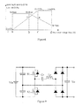
- the schematic diagram of half bridge series resonance circuit shown in Fig. 9 in practical application, it is only needed to perform a process of combining the four output signals PWM1, PWM2, PWM3, PWM4 in groups.
- S1, S2 in the half bridge series resonance circuit in Fig. 9 are modulated with the resultant two outputs respectively.
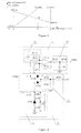
- the present invention includes a pulse-width modulation controlling chip 10.
- COMP terminal and RT terminal of the pulse-width modulation controlling chip 10 are connected to a voltage matching module 2 and a resistance controlling module 3 respectively.
- the voltage matching module 2 and the resistance controlling module 3 provide corresponding controlling parameters to the pulse-width modulation controlling chip 10 in accordance with the input voltage (i.e., the loop circuit Vloop).
- the pulse-width modulation controlling chip 10 modulates the resonance circuit accordingly.
- S1, S2 of the half bridge series resonance circuit are modulated by two output signals PWM1, PWM2 of the phase-shift pulse-width modulation controlling chip 10.
- input voltages of the voltage matching module 2 and the resistance controlling module 3 are both loop circuit voltage Vloop.
- the loop circuit voltage Vloop is an output voltage which is an output voltage of the resonance circuit Vo passing through a sampling circuit and a regulator (such as, PID regulator).
- the voltage matching module 2 includes an operational amplifier U701 and a first voltage dividing sub-module 21.
- a resistor R714 is connected between an inverting terminal of the operational amplifier U701 and the ground, and a resistor R711 is connected between the inverting terminal of the operational amplifier U701 and the output terminal.
- a non-inverting terminal of the operational amplifier U701 is connected to a voltage dividing terminal of the first voltage dividing sub-module 21.
- the first voltage dividing sub-module 21 includes series resistors R712 and R713, and is connected between the loop circuit voltage Vloop and the ground. The junction of resistors R712 and R713 is connected to the non-inverting terminal of the operational amplifier U701 directly.
- a current limiting circuit 22 is connected between an output terminal of the operational amplifier U701 and the COMP terminal in the pulse-width modulation controlling chip 10.
- the current limiting circuit 22 includes series resistors R715, R716 and a capacitor C1.
- the resistors R715, R716 are connected in series between the output terminal of the operational amplifier U701 and the RT terminal, and the capacitor C1 is connected between the junction of the resistor R715 and the resistor R716 and the ground, wherein the capacitor C 1 serves as voltage regulator and filter.
- the voltage matching module 2 matches a width-modulation voltage interval corresponding to the loop circuit voltage Vloop with a voltage range in which the width-modulation is performed for the COMP terminal of the pulse-width modulation controlling chip 10.
- the specific scale parameters in the matching can be set in consideration of parameters of the pulse-width modulation controlling chip 10 and operating parameters of the half bridge series resonance circuit.
- the resistance controlling module 3 includes a second voltage dividing sub-module 31 which includes series resistors R701 and R702, and is connected between the loop circuit voltage Vloop and the ground.
- a resistor R703 is connected between the junction of the resistors R701, R702 and the RT terminal.
- the resistance controlling module 3 is connected between the loop circuit voltage Vloop and the RT terminal of the pulse-width modulation controlling chip 10 such that the equivalent resistance of the RT terminal to the external is regulated accordingly as the loop circuit voltage Vloop changes.
- the resistance controlling module 3 further includes a voltage-comparing sub-module 32.
- the voltage-comparing sub-module 32 generates reference level Vref.
- a first diode D702 is connected between the reference level Vref and the input terminal of the second voltage-dividing sub-module 31, while a second diode D701 is connected between the loop circuit voltage Vloop and the input terminal of the second voltage-dividing sub-module 31, with cathodes of the first diode D702 and the second diode D701 being connected with the second voltage-dividing sub-module 31.
- a precision reference element U702 is applied in the voltage-comparing sub-module 32 to provide the reference level Vref.
- the power supply Vc is divided with resistors R704, R705 and R706, and a voltage drop of the resistor R706 provides operating voltage to the precision reference element U702.
- a filter capacitor C2 is connected between the reference level Vref and the ground.
- the control to the half bridge resonance circuit using pulse-width modulation controlling chip 10 is shown.
- the present invention also can be applied to control a full bridge resonance circuit.
- the schematic diagram of full bridge series resonance circuit shown in Fig.1 in practical application, it only needs to modulate S1, S2, S3, S4 of the full series resonance circuit in Fig.1 with the two output signals PWM1, PWM2 from the pulse-width modulation controlling chip 10 in groups.
- the output signals PWM1 from the pulse-width modulation controlling chip 10 controls S1 and S3 of the full series resonance circuit simultaneously
- the output signals PWM2 from the pulse-width modulation controlling chip 10 controls S2 and S4 of the full bridge series resonance circuit simultaneously.
- the maximum duty ratio of the output pulse from the controlling chip is described as 50%, and two switch tubes of the same bridge arm are turned on complementally, and the overall duty ratio is 1.
- This way of the description is based on the situation in which the dead time of the two drive pulses is not considered. It is necessary to set a certain dead time between the two drive pulses, in order that the two switch tubes of the same bridge arm are not straight through, so in fact, the maximum duty ratio of the output pulse from the controlling chip is certainly smaller than 50%, and two switch tubes of the same bridge arm are turned on complementally, and the overall duty ratio is smaller than 1.
- the dead time between two drive pulses can be regulated by means of design of the circuit. Therefore, the above description shows an ideal state, but this will not limit the circuit design according to the present invention.
Landscapes
- Engineering & Computer Science (AREA)
- Power Engineering (AREA)
- Dc-Dc Converters (AREA)
Applications Claiming Priority (2)
| Application Number | Priority Date | Filing Date | Title |
|---|---|---|---|
| CN2006100747941A CN101056061B (zh) | 2006-04-14 | 2006-04-14 | 一种谐振电路调制控制方法和系统 |
| PCT/CN2007/000509 WO2007118401A1 (fr) | 2006-04-14 | 2007-02-13 | Procédé et système de commande de modulation de circuit syntonique |
Publications (2)
| Publication Number | Publication Date |
|---|---|
| EP2009758A1 true EP2009758A1 (fr) | 2008-12-31 |
| EP2009758A4 EP2009758A4 (fr) | 2009-05-20 |
Family
ID=38609055
Family Applications (1)
| Application Number | Title | Priority Date | Filing Date |
|---|---|---|---|
| EP07710934A Withdrawn EP2009758A4 (fr) | 2006-04-14 | 2007-02-13 | Procédé et système de commande de modulation de circuit syntonique |
Country Status (5)
| Country | Link |
|---|---|
| US (1) | US8284570B2 (fr) |
| EP (1) | EP2009758A4 (fr) |
| CN (1) | CN101056061B (fr) |
| RU (1) | RU2436210C2 (fr) |
| WO (1) | WO2007118401A1 (fr) |
Families Citing this family (23)
| Publication number | Priority date | Publication date | Assignee | Title |
|---|---|---|---|---|
| TW200923631A (en) * | 2007-11-22 | 2009-06-01 | Inventec Corp | Apparatus and method for adjusting working frequency of VRD by detecting current |
| US7660133B1 (en) * | 2008-11-04 | 2010-02-09 | Champion Microelectronic Corporation | Resonant switching converter having operating modes above and below resonant frequency |
| CN101969303B (zh) * | 2010-06-30 | 2013-04-17 | 艾默生网络能源系统北美公司 | 一种谐振电路输出特性控制方法 |
| US8811039B2 (en) * | 2010-07-16 | 2014-08-19 | Virginia Tech Intellectual Properties, Inc. | Pulse width modulated resonant power conversion |
| JP5547603B2 (ja) * | 2010-10-13 | 2014-07-16 | 株式会社日立情報通信エンジニアリング | 電源装置 |
| CN102735941A (zh) * | 2011-04-13 | 2012-10-17 | 鸿富锦精密工业(深圳)有限公司 | 偏置电阻测试装置及偏置电阻测试装置的使用方法 |
| TWI434622B (zh) * | 2011-12-30 | 2014-04-11 | Macroblock Inc | 轉換器之等效電阻值的控制方法與裝置 |
| CN103795252B (zh) * | 2012-10-31 | 2016-02-24 | 中兴通讯股份有限公司 | 一种串联谐振变换器的控制方法 |
| US9263960B2 (en) * | 2013-09-16 | 2016-02-16 | Delta Electronics, Inc. | Power converters for wide input or output voltage range and control methods thereof |
| CN104158411A (zh) * | 2014-08-08 | 2014-11-19 | 华中科技大学 | 一种对高压电容器充电限功率及充电保持控制方法 |
| DE102015004742A1 (de) * | 2015-04-11 | 2016-10-13 | Finepower Gmbh | Verfahren zum Betrieb eines Resonanzkreises |
| CN106300976B (zh) * | 2015-05-19 | 2020-02-07 | 福州瑞芯微电子股份有限公司 | 开关电源的多时钟域控制装置、方法、及一种开关电源 |
| CN106300917A (zh) * | 2016-10-09 | 2017-01-04 | 深圳市钜能科技有限公司 | 负反馈电路 |
| CN108075663A (zh) * | 2016-11-07 | 2018-05-25 | 赤多尼科两合股份有限公司 | 开关电源的控制电路 |
| FR3064829B1 (fr) * | 2017-04-03 | 2019-04-05 | Valeo Siemens Eautomotive France Sas | Procede de protection contre un courant de surpuissance dans un circuit resonnant |
| FR3082680B1 (fr) | 2018-06-15 | 2020-05-29 | Renault S.A.S | Procede de commande en frequence de la tension d'entree d'un convertisseur courant continu-courant continu |
| CN109240399B (zh) * | 2018-10-29 | 2020-10-20 | 北京无线电测量研究所 | 一种用于电源控制的调频/移相复合控制电路 |
| CN109600047B (zh) * | 2018-12-27 | 2021-05-04 | 上海电力学院 | 一种dc/dc电路中llc模块的参数优化方法 |
| TWI694670B (zh) | 2019-02-15 | 2020-05-21 | 群光電能科技股份有限公司 | 諧振式電源轉換裝置 |
| CN111786567A (zh) * | 2020-07-28 | 2020-10-16 | 石家庄通合电子科技股份有限公司 | 用于减小全桥llc变换器间歇时输出纹波的控制方法 |
| DE102020210899A1 (de) * | 2020-08-28 | 2022-03-03 | Festo Se & Co. Kg | Sicherheitsvorrichtung, Ventilanordnung und Verfahren |
| CN115528918B (zh) * | 2021-06-25 | 2026-07-28 | 台达电子工业股份有限公司 | Llc谐振转换器及其控制方法 |
| EP4366149A4 (fr) * | 2021-06-30 | 2024-08-28 | Mitsubishi Electric Corporation | Dispositif de conversion de puissance |
Family Cites Families (17)
| Publication number | Priority date | Publication date | Assignee | Title |
|---|---|---|---|---|
| US4136315A (en) * | 1977-07-27 | 1979-01-23 | Westinghouse Air Brake Company | Low and high frequency oscillators having common voltage regulator circuit |
| US4888821A (en) * | 1988-12-09 | 1989-12-19 | Honeywell Inc. | Synchronization circuit for a resonant flyback high voltage supply |
| US4964028A (en) * | 1989-10-26 | 1990-10-16 | Plessey Electronic Systems Corp. | Current limited quasi-resonant voltage converting power supply |
| JP3547837B2 (ja) * | 1995-03-31 | 2004-07-28 | ミネベア株式会社 | インバ−タ装置 |
| US5754414A (en) * | 1996-02-23 | 1998-05-19 | Hanington; Gary J. | Self-compensating switching power converter |
| US5847942A (en) * | 1996-05-30 | 1998-12-08 | Unitrode Corporation | Controller for isolated boost converter with improved detection of RMS input voltage for distortion reduction and having load-dependent overlap conduction delay of shunt MOSFET |
| IL148862A0 (en) * | 1999-10-01 | 2002-09-12 | Online Power Supply Inc | Non-saturating magnetic element(s) power converters and surge protection |
| RU2159507C1 (ru) * | 1999-10-29 | 2000-11-20 | Аликов Сергей Владимирович | Узел кодирования и/или декодирования информации, система передачи информации с уплотнением каналов, система передачи информации в телекоммуникационной сети |
| CN1118129C (zh) * | 2000-08-01 | 2003-08-13 | 艾默生网络能源有限公司 | 脉冲混合调制型开关电源 |
| CN2433774Y (zh) * | 2000-08-10 | 2001-06-06 | 北京通力环电气有限公司 | 电压谐振软开关变换器的变频变脉宽综合控制器 |
| US6717389B1 (en) * | 2001-12-21 | 2004-04-06 | Unisys Corporation | Method and apparatus for current controlled transient reduction in a voltage regulator |
| JP3800415B2 (ja) * | 2002-07-30 | 2006-07-26 | ミネベア株式会社 | パルス幅変調回路及びそれを用いた照明装置 |
| CN100541992C (zh) * | 2003-09-08 | 2009-09-16 | 艾默生网络能源有限公司 | 串联谐振直流/直流变换器的控制方法及装置 |
| US7498786B2 (en) * | 2003-12-01 | 2009-03-03 | Fairchild Semiconductor Corporation | Digital control of switching voltage regulators |
| JP2005210759A (ja) * | 2004-01-19 | 2005-08-04 | Sanken Electric Co Ltd | 共振型スイッチング電源装置 |
| DE102004006004A1 (de) * | 2004-02-06 | 2005-06-30 | Infineon Technologies Ag | Schaltwandler mit Resonanztopologie |
| WO2007138344A2 (fr) * | 2006-05-26 | 2007-12-06 | Cambridge Semiconductor Limited | Convertisseurs et contrôleurs d'énergie d'avancement |
-
2006
- 2006-04-14 CN CN2006100747941A patent/CN101056061B/zh not_active Expired - Lifetime
-
2007
- 2007-02-13 US US12/297,044 patent/US8284570B2/en not_active Expired - Fee Related
- 2007-02-13 WO PCT/CN2007/000509 patent/WO2007118401A1/fr not_active Ceased
- 2007-02-13 EP EP07710934A patent/EP2009758A4/fr not_active Withdrawn
- 2007-02-13 RU RU2008143194/07A patent/RU2436210C2/ru not_active IP Right Cessation
Also Published As
| Publication number | Publication date |
|---|---|
| CN101056061A (zh) | 2007-10-17 |
| US8284570B2 (en) | 2012-10-09 |
| CN101056061B (zh) | 2012-12-05 |
| US20090303750A1 (en) | 2009-12-10 |
| WO2007118401A1 (fr) | 2007-10-25 |
| RU2436210C2 (ru) | 2011-12-10 |
| EP2009758A4 (fr) | 2009-05-20 |
| RU2008143194A (ru) | 2010-05-20 |
Similar Documents
| Publication | Publication Date | Title |
|---|---|---|
| US8284570B2 (en) | Method and system of syntonic circuit modulation controlling | |
| US5805432A (en) | Resonant DC-DC converter capable of controlling by pulse width modulation | |
| JP3257505B2 (ja) | 圧電トランスインバータ | |
| EP1229634B1 (fr) | Appareil d'alimentation de puissance à découpage | |
| US6396716B1 (en) | Apparatus for improving stability and dynamic response of half-bridge converter | |
| CN102332826B (zh) | 用于反激式电源变换器的初级侧感测和调整的系统和方法 | |
| Lai et al. | A family of continuous-conduction-mode power-factor-correction controllers based on the general pulse-width modulator | |
| US6091234A (en) | Control circuit of a synchronous rectification type DC-DC converter | |
| US5654881A (en) | Extended range DC-DC power converter circuit | |
| EP2380268B1 (fr) | Convertisseur auto-oscillant | |
| US7035125B2 (en) | Switching power supply and control method for the same | |
| US8514594B2 (en) | Method and apparatus for controlling power converter output characteristics | |
| CN101515756A (zh) | 具有多种模式的用于高效功率控制的方法和系统 | |
| US7825605B2 (en) | DA/AC convert for driving cold cathode fluorescent lamp | |
| CN105305783A (zh) | 用于谐振转换器的控制设备 | |
| US20050270814A1 (en) | Modified sinusoidal pulse width modulation for full digital power factor correction | |
| CN101506752B (zh) | 固定关断时间功率因数校正控制器 | |
| US9985520B2 (en) | Pulse width modulator for DC/DC converters | |
| US10560025B2 (en) | Frequency hopping for reducing switching power converter noise | |
| US12587097B2 (en) | Control circuit and control method for multiphase power supply and multiphase power supply | |
| JPH11235023A (ja) | スイッチング・レギュレーター | |
| JPH1014217A (ja) | スイッチング電源回路 | |
| US9985532B1 (en) | Pulse frequency modulation mode transitions for single stage power converter | |
| US6115265A (en) | Constant output current load driver | |
| US10727749B1 (en) | Dual rail power supply system |
Legal Events
| Date | Code | Title | Description |
|---|---|---|---|
| PUAI | Public reference made under article 153(3) epc to a published international application that has entered the european phase |
Free format text: ORIGINAL CODE: 0009012 |
|
| 17P | Request for examination filed |
Effective date: 20081014 |
|
| AK | Designated contracting states |
Kind code of ref document: A1 Designated state(s): AT BE BG CH CY CZ DE DK EE ES FI FR GB GR HU IE IS IT LI LT LU LV MC NL PL PT RO SE SI SK TR |
|
| AX | Request for extension of the european patent |
Extension state: AL BA HR MK RS |
|
| A4 | Supplementary search report drawn up and despatched |
Effective date: 20090420 |
|
| DAX | Request for extension of the european patent (deleted) | ||
| RBV | Designated contracting states (corrected) |
Designated state(s): DE |
|
| RAP1 | Party data changed (applicant data changed or rights of an application transferred) |
Owner name: EMERSON NETWORK POWER, ENERGY SYSTEMS, NORTH AMERI |
|
| 17Q | First examination report despatched |
Effective date: 20091016 |
|
| STAA | Information on the status of an ep patent application or granted ep patent |
Free format text: STATUS: THE APPLICATION IS DEEMED TO BE WITHDRAWN |
|
| 18D | Application deemed to be withdrawn |
Effective date: 20180529 |