EP2009792A2 - Gate-Treibervorrichtung - Google Patents
Gate-Treibervorrichtung Download PDFInfo
- Publication number
- EP2009792A2 EP2009792A2 EP08159117A EP08159117A EP2009792A2 EP 2009792 A2 EP2009792 A2 EP 2009792A2 EP 08159117 A EP08159117 A EP 08159117A EP 08159117 A EP08159117 A EP 08159117A EP 2009792 A2 EP2009792 A2 EP 2009792A2
- Authority
- EP
- European Patent Office
- Prior art keywords
- voltage
- constant
- gate
- current
- circuit
- Prior art date
- Legal status (The legal status is an assumption and is not a legal conclusion. Google has not performed a legal analysis and makes no representation as to the accuracy of the status listed.)
- Granted
Links
Images








Classifications
-
- H—ELECTRICITY
- H03—ELECTRONIC CIRCUITRY
- H03K—PULSE TECHNIQUE
- H03K17/00—Electronic switching or gating, i.e. not by contact-making and –breaking
- H03K17/16—Modifications for eliminating interference voltages or currents
- H03K17/168—Modifications for eliminating interference voltages or currents in composite switches
-
- H—ELECTRICITY
- H03—ELECTRONIC CIRCUITRY
- H03K—PULSE TECHNIQUE
- H03K17/00—Electronic switching or gating, i.e. not by contact-making and –breaking
-
- H—ELECTRICITY
- H03—ELECTRONIC CIRCUITRY
- H03K—PULSE TECHNIQUE
- H03K17/00—Electronic switching or gating, i.e. not by contact-making and –breaking
- H03K17/04—Modifications for accelerating switching
- H03K17/0406—Modifications for accelerating switching in composite switches
-
- H—ELECTRICITY
- H03—ELECTRONIC CIRCUITRY
- H03K—PULSE TECHNIQUE
- H03K17/00—Electronic switching or gating, i.e. not by contact-making and –breaking
- H03K17/06—Modifications for ensuring a fully conducting state
- H03K17/063—Modifications for ensuring a fully conducting state in field-effect transistor switches
-
- H—ELECTRICITY
- H03—ELECTRONIC CIRCUITRY
- H03K—PULSE TECHNIQUE
- H03K17/00—Electronic switching or gating, i.e. not by contact-making and –breaking
- H03K17/08—Modifications for protecting switching circuit against overcurrent or overvoltage
- H03K17/081—Modifications for protecting switching circuit against overcurrent or overvoltage without feedback from the output circuit to the control circuit
- H03K17/0812—Modifications for protecting switching circuit against overcurrent or overvoltage without feedback from the output circuit to the control circuit by measures taken in the control circuit
- H03K17/08128—Modifications for protecting switching circuit against overcurrent or overvoltage without feedback from the output circuit to the control circuit by measures taken in the control circuit in composite switches
-
- H—ELECTRICITY
- H03—ELECTRONIC CIRCUITRY
- H03K—PULSE TECHNIQUE
- H03K17/00—Electronic switching or gating, i.e. not by contact-making and –breaking
- H03K17/16—Modifications for eliminating interference voltages or currents
- H03K17/161—Modifications for eliminating interference voltages or currents in field-effect transistor switches
- H03K17/162—Modifications for eliminating interference voltages or currents in field-effect transistor switches without feedback from the output circuit to the control circuit
- H03K17/163—Soft switching
Definitions
- This invention relates to a gate drive circuit for use in a switching device of voltage drive type, such as IGBT or FET.
- Patent Document 1 JP-A-8-033 315 (Sectors [0008] to [0011] and FIG. 6 )
- Such a prior-art gate drive apparatus has had the problem that a time in which the switching device shifts from OFF to ON varies greatly, depending upon the individual characteristics of elements.
- FIG. 27 is a diagram of the circuit arrangement of the gate drive apparatus, while FIG. 28 is a diagram for explaining the operation thereof.
- a gate drive IC applies the control voltage VDD of a control power source to the gate (G) of an IGBT 1 through a gate resistance Rg and charges a gate input capacitance Cge. On this occasion, the IGBT 1 remains OFF before a gate voltage arrives at a gate threshold voltage (Vth) ([1] in FIG. 28 ).
- the collector current Ic of the IGBT 1 becomes the current I (A) (a period [1] to [2] in FIG. 28 ).
- the charging by the mirror voltage is further required until the voltage Vce thereafter shifts completely into the ON state, and a period therefor depends upon the current Ig (a time point [4] or [4]' in FIG. 28 ).
- the variance of the voltage Vth becomes the variance of the CR charging time and becomes the variance of the Ic ON-shift time (t I - ON ).
- the variances of the voltage Vth and the factor gm become that variance of the mirror voltage, which causes the variance of the charging current and causes the variance of the charging time, so that the Vce ON-shift time (t V - ON ) varies.
- the influence of the variance can be lessened by making the gate resistance value Rg smaller.
- the connection of a gate resistance is indispensable so as to prevent a switching speed from rising excessively.
- EMI countermeasure it is a general disposal to limit "dV/dt" and "dI/dt" at the time of switching.
- the least value of the ON shift time t ON is designed under the condition of the least mirror voltage, and the gate resistance at a switching speed (max) is determined.
- the switching speed at the greatest mirror voltage is calculated under the condition under which the gate resistance has been determined, and the switching loss must be designed on the basis of the corresponding time period. Accordingly, the variance of the loss attributed to the variance of the mirror voltage tends to become large. Incidentally, the situation of an OFF shift is the same, and a similar problem is posed.
- This invention has been made in order to solve the problems as stated above, and it has for its object to obtain a gate drive apparatus which can suppress the variance of switching speeds attributed to the variances of threshold voltages and mirror voltages in a plurality of switching devices to be driven by the gate drive apparatus, and which can minimize the variance of losses.
- a gate drive apparatus concerns a gate drive apparatus which is connected to a gate of a switching device of voltage drive type, and which outputs to the gate, gate signals that turn ON/OFF the switching device on the basis of ON/OFF gate control signals.
- a gate drive apparatus for either or both of the turn-ON operation and the turn-OFF operation includes a constant-current-pulse gate drive circuit which creates the gate signal as a constant-current output, a constant-voltage-pulse gate drive circuit which creates the gate signal as a constant-voltage output, and a decision switch circuit which switches the operation of the constant-current-pulse gate drive circuit and the operation of the constant-voltage-pulse gate drive circuit.
- a shift period in a gate drive mode is driven by the constant-current output, whereby the variance of the shift period attributed to the variances of a gate threshold voltage and a mirror voltage in the switching device can be minimized, and the variances of a switching speed and a switching loss can be sharply suppressed.
- constant-current drive is switched to constant-voltage drive, whereby the switching device can be driven without spoiling the reliability of the gate oxide film thereof.
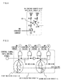
- FIG. 1 is a general configurational diagram of a gate drive apparatus according to Embodiment 1 of the present invention.
- the output of a constant-current-pulse gate drive circuit 2 is connected to the gate of a switching device (IGBT) 1, and the output of a constant-voltage-pulse gate drive circuit 3 is further connected thereto.
- IGBT switching device
- a decision/switch circuit 4 receives as inputs, a control signal (gate control signal) and the gate voltage of the switching device 1 (a gate voltage detection circuit is not shown).
- the decision/switch circuit 4 outputs and connects the control signal of ON constant current/OFF constant current to the constant-current-pulse gate drive circuit 2, and the control signal of ON constant voltage/OFF constant voltage to the constant-voltage-pulse gate drive circuit 3.
- the voltage VDD2 of a control power source used for the constant-current-pulse gate drive circuit 2 is set higher than the voltage VDD1 of a control power source for the constant-voltage-pulse gate drive circuit 3. This is because the variance of constant-current set values attributed to the individual variances of components (semiconductor devices) for use in the constant-current-pulse gate drive circuit 2 is suppressed as will be detailed later.
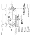
- FIG. 2 shows a chart of the control signal, gate voltage waveforms, and the collector current Ic and collector-emitter voltage Vce of the IGBT in this arrangement.
- the inductive load L is flywheeled by a closed circuit consisting of this load and a diode, with a current I (A).
- an ON constant-current-pulse gate drive circuit 21 operates, and a constant current Ig is supplied to the gate of the switching device 1 so as to perform constant current charging for the gate input capacitance Cge of this switching device.
- the IGBT 1 remains OFF (a time point [1] or [1]' in FIG. 2 ).
- Vth gate threshold voltage
- the collector current Ic of the IGBT 1 becomes the current I (A) (a period [1] to [2], or [1]' to [2]' in FIG. 2 ).
- the gate threshold voltage Vth is a gate voltage at the time when a current of 0.01 % as a ratio to the rated current of the switching element flows through the switching element.
- Qgc mirror charges
- Cgc feedback capacitance
- an OFF operation (turn-OFF operation), accordingly an operation in which "L” (a “low” level) is input as the control signal until the IGBT 1 is turned OFF, will now be described in detail.
- the control signal of the OFF constant current is output by the decision/switch circuit 4.
- an OFF constant-current-pulse gate drive circuit 22 operates, and charges are released from the gate of the switching device 1 by a constant current, so that a gate capacitance (Cge + Cgc) is discharged by the constant current.
- the IGBT 1 remains ON (a period [5] to [6] in FIG. 2 ).
- the storage time of the mirror charges (Qgc) to be stored in the feedback capacitance (Cgc) is the OFF time of the voltage Vce.
- the collector current Ic of the IGBT 1 is shifted into OFF.
- the gate voltage is the mirror voltage, and hence, the collector current Ic of the IGBT 1 is the current I (A).
- the collector current Ic becomes substantially 0 (A) and is shifted into OFF (a period [8] to [9] in FIG. 2 ).
- T I - ⁇ OFF prior art Cge • Rg • ln ⁇ 1 + 1 / Vth • ⁇ Ic / gm . and it depends upon the threshold voltage Vth.
- t I - ⁇ OFF Cge / Ig ⁇ ⁇ Ic / gm . Accordingly, the period becomes independent of the voltage Vth, and the current is shifted into OFF in the fixed time period.
- the device used in FIG. 2 is an example having the following characteristics: In the ON operation, the voltage Vce is abruptly shifted into ON in the period [2] to [3] and is completely shifted into ON (Vcesat) at a time point [4]. Besides, in the OFF operation, the voltage Vce is slowly shifted into OFF in a period [6] to [7] and is abruptly shifted into OFF in a period [7] to [8]. In this regard, there is also a device in which the voltage Vce is shifted with a constant dV/dt in the period [2] to [4] or the period [6] to [8].
- FIG. 3 shows a practicable arrangement example of the ON constant-current-pulse gate drive circuit 21.
- the ON constant-current-pulse gate drive circuit 21 which is capable of constant current drive at a high speed receives an ON constant-current operation command, and outputs a voltage VO at a high speed through the turn-OFF of a switch Q1' and the turn-ON of a switch Q2.
- the base voltage of a transistor Q1 becomes the voltage VO
- the switch Q2 in order to stop a constant current, the switch Q2 is turned OFF, and the switch Q1' is turned ON, whereby to a voltage VDD2 or a voltage of or above the voltage VDD2 is output at a high speed.
- the base current of the transistor Q1 is prevented from flowing, and the transistor Q1 is turned OFF.
- the gate drive circuit 21 can be easily configured by employing high-speed switching devices of low capacitances.
- the ON constant-current-pulse gate drive circuit 21 when the switch Q2 is turned ON by the control signal of the ON constant current, the voltage VO becomes the base voltage of the transistor Q1, and the constant current drive is performed.
- the output voltage of the transistor Q1 becomes the voltage VO or above, the circuit fails to operate with the constant current. Therefore, the voltage VO must be made the greatest mirror voltage or above in which the variance of the switching device 1 to be driven is considered.
- Ic VDD ⁇ 2 - V EB - VO / R ⁇ 3 ⁇ h FE / h FE + 1 .
- the voltage V EB has an individual difference variance, and hence, it forms a cause for the variance of the constant current.
- FIG. 4 shows an ON constant-current-pulse gate drive circuit 21-1 which is a modification to the embodiment in FIG.3 .
- a switch Q2 when a switch Q2 is turned ON, a voltage value VO divided by resistances R1 and R2 becomes the base voltage of a transistor Q1, and the switch Q2 is turned OFF, whereby a voltage VDD2 can be applied to the base of the transistor Q1.
- the gate drive circuit is switched from the constant-current-pulse gate drive circuit 2 to the constant-voltage-pulse gate drive circuit 3, by the decision/switch circuit 4 which observes the gate voltage and which performs the switching control between the constant current drive and the constant voltage drive.
- the power source of the constant-voltage-pulse gate drive circuit 3 is made the voltage VDD1, and the voltage which does not degrade the reliability of the gate oxide film is set.
- FIG. 5 shows an example of the decision/switch circuit 4.
- the decision/switch circuit 4 receives the control signal (gate control signal) "H", it makes an OFF signal inactive and outputs an ON signal.
- the gate voltage of the IGBT 1 is observed. If it is decided by a first decision circuit 41 that the gate voltage is, at most, a voltage VH being a first set value (a value which is the greatest variance value of the mirror voltage, or above is set as the voltage VH), the signal of the ON constant current is output, and when the gate voltage exceeds the first set value VH, the signal of the ON constant current is switched to the signal of the ON constant voltage.
- a voltage VH being a first set value (a value which is the greatest variance value of the mirror voltage, or above is set as the voltage VH)
- the decision/switch circuit 4 when the decision/switch circuit 4 receives the control signal "L", it makes the ON signal inactive and outputs the OFF signal. On this occasion, the gate voltage of the IGBT 1 is observed. If it is decided by a second decision circuit 42 that the gate voltage is, at least, a voltage VL being a second set value (a value which is the least Vth voltage, or below is set as the voltage VL), the signal of the OFF constant current is output, and when the gate voltage becomes less than the second set value VL, the signal of the OFF constant current is switched to the signal of the OFF constant voltage.
- a voltage VL being a second set value (a value which is the least Vth voltage, or below is set as the voltage VL)
- the switching drive control between the constant-current-pulse gate drive circuit 2 and the constant-voltage-pulse gate drive circuit 3 is performed, and any overvoltage is prevented from being applied to the gate.
- the voltage VDD2 may well be made the same as the voltage VDD 1. Also, as practicable examples will be indicated later, it is possible to adopt a scheme in which the constant current drive and the constant voltage drive are switched for only the ON shift or for only the OFF shift.
- Japanese Patent No. 3,680,722 Japanese Patent No. 3,680,722 (refer chiefly to Sectors [0025] to [0027] and FIG. 8 )
- Japanese Patent No. 3,680,722 Japanese Patent No. 3,680,722 (refer chiefly to Sectors [0025] to [0027] and FIG. 8 )
- the inventors studied for reference in pursuing the constant-current drive circuit described above will be introduced below.
- a constant current circuit based on an OP amplifier is used for drive with a constant current, and the operation of suppressing a gate current is performed only in a period in which a current or a voltage changes.
- the response characteristic of the constant current to a command value is not very high in speed, and especially in turning OFF the constant current, it was difficult to attain a characteristic expected by the inventors. This is conjectured to be ascribable to a response rate and an output slew rate within the OP amplifier, the gate characteristic of a MOS-FET to-be-driven, the "supply voltage versus maximum output voltage" characteristic of the OP amplifier, etc.
- a response delay to a constant-current increasing command and a response delay to a constant-current decreasing command (OA) arise, and especially the response delay at the time of the constant-current decreasing command necessitates a long time for the OFF operation of a transistor Q12 shown in FIG. 8 of the patent document, on account of an insufficient slew rate.
- OA constant-current decreasing command
- the high-speed drive circuit of this embodiment as shown in FIG.3 is required.
- the constituent Q1 of the ON constant-current-pulse gate drive circuit 21 is exemplified as the transistor, it may well be replaced with a circuit which uses an FET or the like element being controllable with a current.
- the ON constant-current-pulse gate drive circuit 21-2 in FIG. 6 uses the type of IC drive capable of level conversion, and it outputs the "L" in a constant current operation and performs the constant current operation by resistances R1 to R3 and a transistor Q1.
- the voltage VDD2 is supplied from an IC 1, whereby the transistor Q1 can be instantly turned OFF. Therefore, the OFF speed of the transistor Q1 stated before can be further enhanced.
- the ON constant-current-pulse gate drive circuit 21-3 in FIG. 7 sets the control signal at the "H” in a constant current operation, to turn OFF a switch Q1' and turn ON a switch Q2, and it performs the constant current operation by resistances R1 to R3 and a transistor Q1.
- the control signal is set at the "L” to turn OFF the switch Q2 and turn ON the switch Q1'.
- the voltage VDD2 or the voltage of or above the voltage VDD2 is directly supplied to the base of the transistor Q1 by a current from the switch Q1', whereby the transistor Q1 can be instantly turned OFF, and simultaneously, the output capacitance and feedback capacitance of the transistor Q2 can be charged. Therefore, the OFF speed of the transistor Q1 stated before can be further enhanced.
- a semiconductor switching device such as MOS-FET or transistor is mentioned as an example of each of the switches Q2 and Q1'.
- the OFF constant-current-pulse gate drive circuit 22 for use in the constant-current-pulse gate drive circuit 2 requires a high-speed constant-current drive circuit which is drivable at a high speed and as to which the variance of the gate current Ig is small.
- FIG. 8 shows the OFF constant-current-pulse gate drive circuit 22 which is capable of constant current drive at a high speed.
- a switch Q3' is turned OFF, and a switch Q4 is turned ON, thereby to output a voltage V1 at a high speed.
- the base voltage of a transistor Q3 becomes the voltage V1
- the constant current drive becomes possible as indicated below.
- R ⁇ 6 ⁇ Ib + Ic + V Be V ⁇ 1
- Ib Ic / h FE
- the switch Q4 is turned OFF, and the switch Q3' is turned ON, whereby a common potential (Vcom) voltage or a voltage of or below the potential Vcom is output at a high speed.
- Vcom common potential
- the base current of the transistor Q3 is prevented from flowing, and the transistor Q3 is turned OFF.
- the common potential (Vcom) 0 V is held in the above formula.
- the gate drive circuit 22 can be easily configured by employing high-speed switching devices of low capacitances.
- the variance of the gate current Ig (indicated as "Ic" in FIG. 8 ) can be suppressed by lowering the potential Vcom of the constant-current drive circuit to or below 0 V. The reason why the variance can be suppressed, will be explained below.
- the voltage V1 becomes the base voltage of the transistor Q3, and the constant current drive is performed.
- the circuit fails to operate with the constant current. Therefore, the voltage V1 must be made the least Vth voltage or below in which the variance of the switching device 1 to be driven is considered.
- Ic V ⁇ 1 - Vcom - V EB / R ⁇ 6 ⁇ h FE / h FE + 1 .
- the voltage V EB has an individual difference variance, and hence, it forms a cause for the variance of the constant current.
- Vcom 0 V
- V1 4.5 V
- V EB 0.8 to 1.0 V
- the constituent Q3 of the OFF constant-current-pulse gate drive circuit 22 is exemplified as the transistor, it may well be replaced with a circuit which uses an FET or the like element being controllable with a current.
- FIG. 9 shows an OFF constant-current-pulse gate drive circuit 22-1 which is a modification to the embodiment in FIG. 8 .
- a transistor Q4 when a transistor Q4 is turned ON, an OFF constant current signal is current-amplified by a voltage follower, a voltage value V1 divided by resistances R4 and R5 becomes the base voltage of a transistor Q3, and the transistor Q4 is turned OFF, whereby a voltage Vcom can be applied to the base of the transistor Q3.
- the voltage Vcom may well be set at a minus voltage, not at the emitter voltage of the switching device 1, in order to decrease the variance of the constant current in consideration of the variance of the voltage V BE .
- the OFF constant-current-pulse gate drive circuit 22-2 in FIG. 10 adopts a configuration in which the control signal of an OFF constant current is buffered by a device IC1, thereby to attain an output voltage precision and to obtain a drive current.
- a circuit current for the voltage division of resistances R4 and R5, and the base current Ib of a transistor Q3 are required as the drive current.
- the OFF constant-current-pulse gate drive circuit 22-3 in FIG. 11 sets the control signal at the level “H” so as to turn OFF a switch Q3' and turn ON a switch Q4 in a constant current operation, and it performs the constant current operation by resistances R4 to R6 and a transistor Q3.
- the control signal is set at the level "L” to turn OFF the switch Q4 and turn ON the switch Q3'.
- the voltage Vcom or the voltage of or less than the voltage Vcom is directly supplied to the base of the transistor Q3 by a current to the switch Q3', whereby the transistor Q3 can be instantly turned OFF, and simultaneously, the output capacitance and feedback capacitance of the switch Q4 can be charged. Therefore, the OFF speed of the transistor Q3 stated before can be further enhanced.
- a semiconductor switching device such as MOS-FET or transistor is mentioned as an example of each of the switches Q4 and Q3'.
- V BE + R6 ⁇ Ie the variance of the voltage V BE
- V BE + R6 ⁇ Ie the variance of the voltage V BE
- a common potential indicated by a mark ⁇ is set at a minus voltage, not at the emitter voltage of the switching device 1, in order to decrease the variance of the constant current.
- the invention can achieve remarkable advantages not existing in the prior art, as follows: At the transient stage of turn-ON, turn-OFF or the like, the gate is driven with the constant current, whereby the variance of a shift period attributed to the variances of the gate threshold voltage Vth and the mirror voltage can be suppressed to the minimum, and the variances of the switching speed and the switching loss can be sharply reduced. Further, the device can be driven without spoiling the reliability of the gate oxide film thereof, by switching the constant current drive to the constant voltage drive.
- the constant-current-pulse gate drive circuits have been used for both the turn-ON and the turn-OFF, but if necessary, such a circuit can be used only at the turn-ON or only at the turn-OFF.
- a configurational example which switches the constant current drive and the constant voltage drive at the ON shift only, will be described below.
- a variance in the ON mode becomes problematic, or a variance in the OFF mode becomes problematic.
- a boosting converter is operated in a discontinuous mode
- hard switching is performed in the OFF mode. Therefore, the variance in the OFF mode is suppressed, and the variance of the switching loss is suppressed.
- the ON mode the abrupt change of a voltage is involved, but a current for the charging of a boosting inductance changes much more slowly than the switching speed. Therefore, no problem is posed even when the ON constant-current drive circuit is not disposed.
- the variance in the ON mode becomes problematic, and the loss/performance of the pulse generator are not influenced even when the variance arises in the OFF mode. In this case, therefore, the OFF constant-current drive circuit is unnecessary.
- inverter drive in a case where the IGBT is subjected to a lifetime control and where the voltage Vcesat is lowered, a tail current flows in spite of the OFF constant-current drive, and the advantage of the constant current drive is sometimes unattainable. Also in such a case, the OFF constant-current drive circuit is unnecessary, and an amount in which the loss varies due to the variance in the OFF mode may be suppressed by suppressing the variance by the ON constant-current drive circuit.
- FIG. 12 shows a gate drive apparatus which switches constant current drive and constant voltage drive in a turn-ON mode.
- a constant-current-pulse gate drive circuit 2' uses an ON constant-current-pulse gate drive circuit 21 which drives a switching device 1 with a constant current in only the ON mode.
- a decision/switch circuit 4' receives as inputs, a control signal (gate control signal) and the gate voltage of the switching device 1, and it outputs the control signal of the ON constant current, the control signal of an ON constant voltage and the control signal of an OFF constant voltage.
- a supply voltage VDD2 is set higher than a supply voltage VDD1, so as to suppress the variance of a constant-current set value attributed to the individual variances of components used in the constant-current drive circuit.
- FIG. 13 A practicable example of the decision/switch circuit 4' is shown in FIG. 13 .
- the decision/switch circuit 4' receives the control signal "H”, it makes the OFF signal inactive and outputs the ON signal.
- the gate voltage of the IGBT 1 is observed. If the gate voltage is, at most, a voltage VH (a value which is the greatest mirror voltage, or above is set as the voltage VH), the control signal of the ON constant current is output, and when the gate voltage becomes greater than the set value VH, the signal of the ON constant current is switched to the control signal of the ON constant voltage.
- VH a value which is the greatest mirror voltage, or above
- This configuration is usable in a case where the stabilization of a switching speed in the turn-ON mode and the reduction of the variance of a switching loss in the turn-ON mode are important. Owing to this configuration, remarkable advantages not existing in the prior art can be achieved as follows: At the transient stage of the turn-ON, the gate is driven with the constant current, whereby the variance of a shift period attributed to the variances of the gate threshold voltage Vth and the mirror voltage can be suppressed to the minimum, and the variances of the switching speed and the switching loss can be sharply reduced. Further, the device can be driven without spoiling the reliability of the gate oxide film thereof, by switching the constant current drive to the constant voltage drive.
- FIG. 14 shows a gate drive apparatus which switches constant current drive and constant voltage drive in a turn-OFF mode.
- a constant-current-pulse gate drive circuit 2'' uses an OFF constant-current-pulse gate drive circuit 22 which drives a switching device 1 with a constant current in only the OFF mode.
- a decision/switch circuit 4" receives as inputs, a control signal (gate control signal) and the gate voltage of the switching device 1, and it outputs the control signal of the OFF constant current, the control signal of an ON constant voltage and the control signal of an OFF constant voltage.
- a common potential of mark V as is used in the constant-current-pulse gate drive circuit 2" may well be set at a minus voltage in order to decrease the variance of the constant current.
- FIG. 15 A practicable example of the decision/switch circuit 4" in this case is shown in FIG. 15 .
- the decision/switch circuit 4" receives the control signal (gate control signal) "H”, it makes the OFF signal inactive and outputs the control signal of the ON constant voltage.
- the decision/switch circuit 4" receives the control signal "L”, it makes the ON signal inactive and outputs the OFF signal.
- the gate voltage of the IGBT 1 is observed.
- the control signal of the OFF constant current is output, and when the gate voltage becomes less than the set value VL, the signal of the OFF constant current is switched to the control signal of the OFF constant voltage.
- This configuration is usable in a case where the stabilization of a switching speed in the turn-OFF mode and the reduction of the variance of a switching loss in the turn-OFF mode are important. Owing to this configuration, it is possible to achieve such a remarkable advantage, not existing in the prior art, that the gate is driven with the constant current at the transient stage of the turn-OFF, whereby the variance of a shift period attributed to the variances of the gate threshold voltage Vth and the mirror voltage can be suppressed to the minimum, and the variances of the switching speed and the switching loss can be sharply reduced.
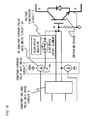
- Embodiment 1 in a case where the switching from the constant current drive to the constant voltage drive needs to be performed at a high speed and where (VDD2 > recommended gate voltage of the IGBT) is set on account of the response delays of the decision/switch circuit 4 and the constant-current-pulse gate drive circuit 2, the overvoltage is applied to the gate of the IGBT 1. It is accordingly apprehended that the reliability of the gate oxide film will degrade, and that the gate breakdown will be induced in the worst case. Therefore, a voltage limitation circuit 5 shown in FIG. 16 is mounted between the ON constant-current-pulse gate drive circuit 21 and the gate terminal of the IGBT 1.
- the voltage limitation circuit 5 observes the gate signal at the output end thereof, and it turns OFF a high-speed cutoff element when the gate signal has become, at least, a prescribed voltage.
- the voltage limitation circuit 5 may well be controlled so as to continue a cutoff state during the OFF operation period, in interlocking with the control signal.
- a circuit example is shown in FIG. 17 .
- a constituent Q5 for the voltage limitation circuit 5 is configured using an FET of high operating speed and low threshold voltage Vth.
- the source terminal of the FET Q5 is connected to the gate terminal of the IGBT 1, whereby the source voltage of the FET Q5 does not become a voltage applied to the gate of the FET Q5, or above.
- a voltage V2 joined to the gate of the FET Q5 is set at a voltage to be output and protected as is divided by resistances R7 and R8, whereby the gate of the IGBT 1 can be protected even in a case where the collector side output voltage of a transistor Q1 has risen more than is supposed, on account of the OFF delay of the transistor Q1 and the response delay of the decision/switch circuit 4.
- the gate voltage of the FET Q5 is strongly influenced by the gate voltage of the IGBT 1 at the source terminal of the FET Q5, it needs to be stabilized by a capacitance C 1 or the like.
- the voltage division by the resistances R7 and R8 is unnecessary, but the gate voltage needs to be stabilized by the capacitance C 1 or the like.
- the ON constant-current-pulse gate drive circuit 21-1 is used as an example of the ON constant-current-pulse gate drive circuit, but another constant-current-pulse gate drive circuit may well be used. Further, even when the voltage limitation circuit 5 is used for the constant-voltage-pulse gate drive circuit 3, similar advantages are obtained, and the gate of the IGBT 1 can be protected. Besides, the use of the voltage limitation circuit 5 is not restricted to the configuration shown by circuit blocks in FIG. 16 .
- FIG. 18 shows an example of the general circuit arrangement of the gate drive apparatus realizing Embodiment 2.
- the variance of the voltage V EB of the transistor Q1 and the temperature characteristic can form causes for the constant-current variance of the constant-current-pulse gate drive circuit 2.
- Embodiment 3 suppresses the characteristic fluctuations of the transistor Q1 and the like semiconductor devices themselves constituting the constant-current-pulse gate drive circuit 21.
- the transistor Q1 and a constituent D1 (or Q1") being a compensating semiconductor device are configured under the same conditions within an identical IC chip.
- the transistor Q1 and the diode D1 or the transistor Q1" are manufactured under the same conditions in the identical IC or chip, whereby the transistor Q1 exhibits a variance characteristic in which the variance direction of the voltage V EB agrees (when the voltage V EB increases, a voltage V F " increases), and an individual difference variance can be compensated. Besides, temperature conditions agree, whereby a temperature compensation becomes possible, and a constant current characteristic can be improved against a temperature change.
- Embodiment 4 permits the switching of the constant current output based on the constant-current-pulse gate drive circuit 2 in the foregoing embodiment 1, whereby a more excellent running characteristic can be obtained in accordance with a running condition.
- a radiation noise level and losses are changed by switching in some running conditions. More specifically, when a switching speed is raised, the noise level becomes high, but the turn-ON loss and turn-OFF loss decrease. When the switching speed is lowered for a radio wave noise countermeasure, the turn-ON loss and the turn-OFF loss increase. That is, it can be the that the noise and the switching speed are in the relationship of trade-off.
- FIGS. 21 and 22 show this embodiment 4.
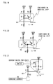
- a configuration in FIG. 21 is such that the ON constant-current-pulse gate drive circuit 21-1 is provided with a current switch portion 211 in which at least one set consisting of a switch SW1 and a resistance R3' is mounted in parallel with a resistance R3 for setting a constant current, and which is a current switch circuit for performing the switching drive of a constant-current output value.
- FIG. 22 An OFF side is similarly configured, and a configuration in FIG. 22 is such that the OFF constant-current-pulse gate drive circuit 22-1 is provided with a current switch portion 221 in which at least one set consisting of a switch SW2 and a resistance R6' is mounted in parallel with a resistance R6 for setting a constant current, and which is a current switch circuit for performing the switching drive of a constant-current output value.
- FIG. 23 A drive timing chart in the case where the current switch portions 211 and 221 are mounted, is shown in FIG. 23 .
- the switching speed is varied by the gate drive apparatus in which the switching speed based on the constant-current drive is stabilized, whereby the trade-off relationship of the noise and the switching losses can be dynamically controlled.
- the switching speed is permitted to control the switching speed in accordance with the running condition. Concretely, in the running region/condition where the radiation noise level ascribable to the switching noise becomes high, the switching speed is lowered to suppress the appearance of the noise. Besides, in the running region/condition where the radiation noise level ascribable to the switching noise becomes low, the switching speed is raised to decrease the losses.
- Embodiment 4 is applicable, not only to the motor load, but also to an inductance or capacitive load and a resistance load, by switching the switching speeds between in a running condition in which the noise of the load is liable to appear and in a running condition in which the noise is less liable to appear.
- the configuration in FIG. 21 can be used as a configuration which completely cuts off unsupposed current supply ascribable to the delay of the current OFF operation based on the transistor Q1.
- the gist of this use will be explained below.
- the constant-current-pulse gate drive circuit 2 has the constant current of the gate drive mode set by the resistance R3', and it is so operated that, at the timing of the stop of the constant current output, the switch SW1 is turned OFF, whereupon the resistance R3' determining the constant current is instantly switched to the resistance R3, whereby the current of the constant-current drive circuit attributed to the OFF delay thereof is prevented from influencing the gate circuit.
- the "switch” signal is turned OFF to turn OFF the switch SW1.
- the "switch” signal is turned ON to turn ON the switch SW1, in consideration of the OFF delay time.
- the OFF delay of the transistor Q1 can be improved.
- This embodiment 5 eliminates the above drawbacks, and it bestows so-called "hysteresis characteristics" on the first decision circuit 41 and the second decision circuit 42 which are used in the foregoing decision/switch circuit 4, etc.
- FIG. 24 shows the first decision circuit 41 which is furnished with a first set value alteration circuit 51.
- a first set value VH: a value of or above the greatest variance value of a mirror voltage is set
- VH a value of or above the greatest variance value of a mirror voltage is set
- FIG. 25 shows the second decision circuit 42 which is furnished with a second set value alteration circuit 52.
- VL a value of or below the least threshold voltage Vth is set
- FIG. 26 shows a decision circuit 43 in Embodiment 6, in which a set value alteration circuit 53 is disposed.
- the upper limit value of the hysteresis characteristics in the preceding embodiment 5 is set at the value VH (the value of or above the greatest variance value of the mirror voltage), and the lower limit value at the value VL (the value of or below the least threshold voltage Vth), whereby a VH decision and a VL decision are output by the single decision circuit 43.
- the output of a comparator rises from the "L” to the “H” to output the VH decision, whereby the constant-current drive is switched to the constant-voltage drive.
- a constituent Q53 is turned ON to alter the set value to the value VL.
- the output of the comparator lowers from the "H” to the “L” to output the VL decision, whereby the constant-current drive is switched to the constant-voltage drive.
- the constituent Q53 is turned OFF to alter the set value to the value VH.
- the operation can be limited to one time of constant-current drive per gate drive pulse, the malfunction in which the current is supplied from the constant-current-pulse gate drive circuit again is preventable when the gate voltage lowers due to the operation of the external gate voltage limitation circuit in an arm short-circuit or overload protection operation.
- Embodiment 1 can be decreased to the single circuit.
Landscapes
- Power Conversion In General (AREA)
- Electronic Switches (AREA)
Applications Claiming Priority (1)
| Application Number | Priority Date | Filing Date | Title |
|---|---|---|---|
| JP2007168849A JP5138287B2 (ja) | 2007-06-27 | 2007-06-27 | ゲート駆動装置 |
Publications (3)
| Publication Number | Publication Date |
|---|---|
| EP2009792A2 true EP2009792A2 (de) | 2008-12-31 |
| EP2009792A3 EP2009792A3 (de) | 2009-03-04 |
| EP2009792B1 EP2009792B1 (de) | 2015-03-25 |
Family
ID=39766998
Family Applications (1)
| Application Number | Title | Priority Date | Filing Date |
|---|---|---|---|
| EP08159117.4A Ceased EP2009792B1 (de) | 2007-06-27 | 2008-06-26 | Gate-Treibervorrichtung |
Country Status (5)
| Country | Link |
|---|---|
| US (1) | US8138818B2 (de) |
| EP (1) | EP2009792B1 (de) |
| JP (1) | JP5138287B2 (de) |
| KR (1) | KR101000587B1 (de) |
| CN (1) | CN101335484B (de) |
Cited By (9)
| Publication number | Priority date | Publication date | Assignee | Title |
|---|---|---|---|---|
| TWI456549B (zh) * | 2011-06-09 | 2014-10-11 | Mitsubishi Electric Corp | 閘極驅動電路 |
| US9490688B2 (en) | 2012-10-22 | 2016-11-08 | Conti Temic Microelectronic Gmbh | Method and circuit arrangement for switching a semiconductor switch |
| US9960755B2 (en) | 2016-05-16 | 2018-05-01 | Dialog Semiconductor (Uk) Limited | Low voltage switching gate driver under a high voltage rail |
| US10734882B2 (en) | 2018-02-09 | 2020-08-04 | Delta Electronics, Inc. | Conversion circuit |
| US10784770B2 (en) | 2018-02-09 | 2020-09-22 | Delta Electronics, Inc. | Conversion circuit |
| US10784795B1 (en) | 2019-08-21 | 2020-09-22 | Delta Electronics, Inc. | Conversion circuit |
| US10784768B2 (en) | 2018-02-09 | 2020-09-22 | Delta Electronics, Inc. | Conversion circuit and conversion circuitry |
| EP3683941A3 (de) * | 2018-12-28 | 2020-10-07 | Delta Electronics, Inc. | Umsetzungsschaltung |
| US11309887B2 (en) | 2018-02-09 | 2022-04-19 | Delta Electronics, Inc. | Conversion circuit |
Families Citing this family (108)
| Publication number | Priority date | Publication date | Assignee | Title |
|---|---|---|---|---|
| US9197132B2 (en) | 2006-12-01 | 2015-11-24 | Flextronics International Usa, Inc. | Power converter with an adaptive controller and method of operating the same |
| JP2009071956A (ja) * | 2007-09-12 | 2009-04-02 | Mitsubishi Electric Corp | ゲート駆動回路 |
| WO2010083514A1 (en) | 2009-01-19 | 2010-07-22 | Flextronics International Usa, Inc. | Controller for a power converter |
| US9019061B2 (en) | 2009-03-31 | 2015-04-28 | Power Systems Technologies, Ltd. | Magnetic device formed with U-shaped core pieces and power converter employing the same |
| WO2010134276A1 (ja) * | 2009-05-19 | 2010-11-25 | 三菱電機株式会社 | ゲート駆動回路 |
| US9077248B2 (en) | 2009-06-17 | 2015-07-07 | Power Systems Technologies Ltd | Start-up circuit for a power adapter |
| US8643222B2 (en) | 2009-06-17 | 2014-02-04 | Power Systems Technologies Ltd | Power adapter employing a power reducer |
| US8638578B2 (en) | 2009-08-14 | 2014-01-28 | Power System Technologies, Ltd. | Power converter including a charge pump employable in a power adapter |
| CN102498668A (zh) * | 2009-09-15 | 2012-06-13 | 三菱电机株式会社 | 栅极驱动电路 |
| US8976549B2 (en) | 2009-12-03 | 2015-03-10 | Power Systems Technologies, Ltd. | Startup circuit including first and second Schmitt triggers and power converter employing the same |
| US9246391B2 (en) | 2010-01-22 | 2016-01-26 | Power Systems Technologies Ltd. | Controller for providing a corrected signal to a sensed peak current through a circuit element of a power converter |
| US8787043B2 (en) | 2010-01-22 | 2014-07-22 | Power Systems Technologies, Ltd. | Controller for a power converter and method of operating the same |
| WO2011116225A1 (en) | 2010-03-17 | 2011-09-22 | Power Systems Technologies, Ltd. | Control system for a power converter and method of operating the same |
| JP2011211836A (ja) * | 2010-03-30 | 2011-10-20 | Panasonic Corp | スイッチングデバイス駆動装置および半導体装置 |
| US20110273220A1 (en) * | 2010-05-04 | 2011-11-10 | Feng Lin | Optimal mosfet driver circuit for reducing electromagnetic interference and noise |
| JP2011250603A (ja) * | 2010-05-27 | 2011-12-08 | Jtekt Corp | モータ制御装置及び電動パワーステアリング装置 |
| JP5678498B2 (ja) * | 2010-07-15 | 2015-03-04 | 富士電機株式会社 | 電力用半導体素子のゲート駆動回路 |
| JP5252055B2 (ja) * | 2010-11-22 | 2013-07-31 | 株式会社デンソー | 負荷駆動装置 |
| US8766671B2 (en) * | 2010-11-22 | 2014-07-01 | Denso Corporation | Load driving apparatus |
| US8633755B2 (en) | 2010-11-22 | 2014-01-21 | Denso Corporation | Load driver with constant current variable structure |
| JP5282782B2 (ja) * | 2010-12-14 | 2013-09-04 | 株式会社デンソー | スイッチング素子の駆動回路 |
| JP5617591B2 (ja) * | 2010-12-14 | 2014-11-05 | 株式会社デンソー | スイッチング素子の駆動装置 |
| JP5617605B2 (ja) * | 2010-12-22 | 2014-11-05 | 株式会社デンソー | スイッチング素子の駆動回路 |
| JP5282790B2 (ja) * | 2011-01-12 | 2013-09-04 | 株式会社デンソー | 電子装置 |
| US8497714B2 (en) * | 2011-01-14 | 2013-07-30 | Infineon Technologies Austria Ag | System and method for driving a switch transistor |
| JP5724397B2 (ja) * | 2011-01-14 | 2015-05-27 | 株式会社デンソー | スイッチング素子の駆動回路 |
| JP5392577B2 (ja) * | 2011-01-28 | 2014-01-22 | 株式会社デンソー | 電子装置 |
| JP5392578B2 (ja) * | 2011-01-28 | 2014-01-22 | 株式会社デンソー | 電子装置 |
| US20120242376A1 (en) * | 2011-03-24 | 2012-09-27 | Denso Corporation | Load drive apparatus and semiconductor switching device drive apparatus |
| US8792257B2 (en) | 2011-03-25 | 2014-07-29 | Power Systems Technologies, Ltd. | Power converter with reduced power dissipation |
| JP5344056B2 (ja) | 2011-03-28 | 2013-11-20 | 株式会社デンソー | スイッチング素子の駆動回路 |
| WO2012153459A1 (ja) * | 2011-05-11 | 2012-11-15 | 富士電機株式会社 | 絶縁ゲート型スイッチング素子の駆動回路 |
| JP2012249377A (ja) * | 2011-05-26 | 2012-12-13 | Sanken Electric Co Ltd | ゲート駆動回路 |
| JP2013005231A (ja) * | 2011-06-16 | 2013-01-07 | Toyota Central R&D Labs Inc | 駆動装置 |
| KR101242985B1 (ko) * | 2011-06-27 | 2013-03-18 | 엘에스산전 주식회사 | 멀티 스테이지 능동 구동 드라이버. |
| JP5701176B2 (ja) * | 2011-08-04 | 2015-04-15 | 三菱電機株式会社 | ゲート駆動装置 |
| US8792256B2 (en) | 2012-01-27 | 2014-07-29 | Power Systems Technologies Ltd. | Controller for a switch and method of operating the same |
| JP5477407B2 (ja) | 2012-02-16 | 2014-04-23 | 株式会社デンソー | ゲート駆動回路 |
| JP5777537B2 (ja) * | 2012-02-17 | 2015-09-09 | 三菱電機株式会社 | パワーデバイス制御回路およびパワーデバイス回路 |
| JP5881477B2 (ja) * | 2012-03-06 | 2016-03-09 | 三菱電機株式会社 | スイッチング素子駆動回路 |
| US9030054B2 (en) * | 2012-03-27 | 2015-05-12 | Raytheon Company | Adaptive gate drive control method and circuit for composite power switch |
| JP5961042B2 (ja) * | 2012-05-28 | 2016-08-02 | ローム株式会社 | ブリッジ出力回路およびそれを用いたモータ駆動装置、電子機器 |
| US9190898B2 (en) | 2012-07-06 | 2015-11-17 | Power Systems Technologies, Ltd | Controller for a power converter and method of operating the same |
| JP5716711B2 (ja) | 2012-07-20 | 2015-05-13 | 株式会社デンソー | スイッチング素子の駆動回路 |
| US9240712B2 (en) | 2012-12-13 | 2016-01-19 | Power Systems Technologies Ltd. | Controller including a common current-sense device for power switches of a power converter |
| JP5811108B2 (ja) | 2013-01-22 | 2015-11-11 | 株式会社デンソー | 電子装置 |
| JP5741605B2 (ja) | 2013-02-04 | 2015-07-01 | 株式会社デンソー | 電子装置 |
| JP5500283B2 (ja) * | 2013-02-28 | 2014-05-21 | 株式会社デンソー | スイッチング素子の駆動回路およびその製造方法 |
| JP5794246B2 (ja) * | 2013-03-11 | 2015-10-14 | 株式会社デンソー | ゲート駆動回路 |
| DE102013104899B4 (de) * | 2013-05-13 | 2020-04-02 | Power Systems Technologies, Ltd. | Steuerung für einen Schalter und Verfahren zu dessen Betrieb sowie Leistungswandler mit derartiger Steuerung |
| KR101706901B1 (ko) | 2013-06-24 | 2017-02-14 | 미쓰비시덴키 가부시키가이샤 | 파워 반도체소자의 구동 회로 |
| KR102111651B1 (ko) | 2013-10-31 | 2020-05-18 | 삼성디스플레이 주식회사 | 표시 장치 및 그 구동 방법 |
| US9300206B2 (en) | 2013-11-15 | 2016-03-29 | Power Systems Technologies Ltd. | Method for estimating power of a power converter |
| CN103716036B (zh) * | 2013-12-05 | 2016-05-11 | 中国航天科技集团公司第九研究院第七七一研究所 | 高速高输出幅值的驱动电路 |
| KR102112299B1 (ko) * | 2014-01-10 | 2020-05-18 | 삼성전자주식회사 | 파워 스위치 소자의 구동 방법 및 구동 회로 |
| JP6197685B2 (ja) | 2014-02-19 | 2017-09-20 | 株式会社デンソー | ゲート駆動回路 |
| CN104880657B (zh) * | 2014-02-28 | 2018-01-12 | 西安永电电气有限责任公司 | Igbt器件的故障检测方法及相应的检测电路 |
| JP6483997B2 (ja) * | 2014-10-10 | 2019-03-13 | ローム株式会社 | パワー半導体駆動回路、パワー半導体回路、及びパワーモジュール回路装置 |
| JP6320273B2 (ja) * | 2014-10-27 | 2018-05-09 | 三菱電機株式会社 | 駆動回路 |
| CN104362935B (zh) * | 2014-11-10 | 2016-12-07 | 无锡普雅半导体有限公司 | 一种抑制电流脉冲的功率驱动电路 |
| US9425786B2 (en) | 2014-11-17 | 2016-08-23 | General Electric Company | System and method for driving a power switch |
| CN104659757B (zh) * | 2014-12-25 | 2018-02-16 | 深圳青铜剑科技股份有限公司 | 一种igbt过压保护电路及一种igbt过压保护方法 |
| US10148264B2 (en) * | 2015-02-16 | 2018-12-04 | Mitsubishi Electric Corporation | Semiconductor device drive circuit |
| JP6882976B2 (ja) | 2015-05-13 | 2021-06-02 | ヌヴォトンテクノロジージャパン株式会社 | スイッチング制御回路 |
| JP6252561B2 (ja) * | 2015-07-28 | 2017-12-27 | トヨタ自動車株式会社 | 電気回路 |
| JP6468150B2 (ja) | 2015-09-29 | 2019-02-13 | 株式会社デンソー | 負荷駆動装置 |
| US9590609B1 (en) | 2015-11-11 | 2017-03-07 | Delphi Technologies Inc. | Gate driver with short circuit protection |
| ITUB20160122A1 (it) | 2016-01-29 | 2017-07-29 | St Microelectronics Srl | Circuito di pilotaggio per un transistor di potenza a effetto di campo, relativo sistema e circuito integrato |
| CN108781043B (zh) * | 2016-03-16 | 2020-05-01 | 松下知识产权经营株式会社 | 电力变换电路 |
| JP6659427B2 (ja) * | 2016-03-31 | 2020-03-04 | ルネサスエレクトロニクス株式会社 | 半導体装置 |
| JP6634329B2 (ja) * | 2016-04-01 | 2020-01-22 | ルネサスエレクトロニクス株式会社 | 半導体装置 |
| US10071652B2 (en) * | 2016-05-11 | 2018-09-11 | Ford Global Technologies, Llc | Dual mode IGBT gate drive to reduce switching loss |
| US10985644B1 (en) | 2016-06-25 | 2021-04-20 | Active-Semi, Inc. | Optimized gate driver for low voltage power loss protection system |
| US10020723B1 (en) | 2016-06-25 | 2018-07-10 | Active-Semi, Inc. | Power loss protection integrated circuit with autonomous capacitor health check |
| US10090675B1 (en) | 2016-06-25 | 2018-10-02 | Active-Semi, Inc. | Fast settlement of supplement converter for power loss protection system |
| US10826480B1 (en) * | 2016-07-01 | 2020-11-03 | Active-Semi, Inc. | Gate driver to decrease EMI with shorter dead-time |
| US9837887B1 (en) * | 2016-08-01 | 2017-12-05 | Ford Global Technologies, Llc | IGBT gate drive with active turnoff to reduce switching loss |
| US10135432B2 (en) * | 2016-09-07 | 2018-11-20 | Texas Instruments Incorporated | Methods and apparatus for low current control for a power connection |
| US9960692B2 (en) | 2016-09-30 | 2018-05-01 | Stmicroelectronics S.R.L. | Driver for a power field-effect transistor with a programmable drive voltage, and related systems and methods |
| US10756720B2 (en) * | 2016-10-17 | 2020-08-25 | Infineon Technologies Ag | Driver circuit for electronic switch |
| JP6601372B2 (ja) * | 2016-11-25 | 2019-11-06 | 株式会社デンソー | ゲート駆動装置 |
| CN109997297A (zh) * | 2016-11-25 | 2019-07-09 | 株式会社电装 | 栅极驱动装置 |
| JP6638628B2 (ja) * | 2016-11-25 | 2020-01-29 | 株式会社デンソー | ゲート駆動装置 |
| JP6889047B2 (ja) * | 2017-06-30 | 2021-06-18 | ローム株式会社 | スイッチング制御回路 |
| KR102284186B1 (ko) * | 2017-07-13 | 2021-08-02 | 한국전기연구원 | 전력용 mosfet 게이트 구동회로 |
| CN111133664A (zh) * | 2017-10-03 | 2020-05-08 | 三菱电机株式会社 | 开关元件的驱动电路、电力变换装置、电梯装置以及开关元件的驱动方法 |
| EP3618278A1 (de) * | 2018-08-28 | 2020-03-04 | Siemens Aktiengesellschaft | Betreiben eines bipolartransistors mit isolierter gate-elektrode |
| US10651723B1 (en) * | 2018-10-22 | 2020-05-12 | Infineon Technologies Austria Ag | Method for static gate clamping in multi-output gate driver systems |
| JP6962308B2 (ja) | 2018-12-10 | 2021-11-05 | 株式会社デンソー | ゲート駆動回路 |
| US11695409B2 (en) * | 2019-04-09 | 2023-07-04 | Mitsubishi Electric Corporation | Drive circuit of power semiconductor element |
| JP2021005950A (ja) * | 2019-06-26 | 2021-01-14 | 株式会社デンソー | トランジスタ駆動回路及びトランジスタのゲート電圧制御方法 |
| US10998843B2 (en) | 2019-09-23 | 2021-05-04 | Power Integrations, Inc. | External adjustment of a drive control of a switch |
| US11206016B2 (en) * | 2019-09-27 | 2021-12-21 | Analog Devices International Unlimited Company | Gate driver with pulsed gate slew control |
| JP7366678B2 (ja) * | 2019-10-02 | 2023-10-23 | ローム株式会社 | ドライブ装置、半導体装置及び電子機器 |
| CN114208037A (zh) * | 2020-02-19 | 2022-03-18 | 富士电机株式会社 | 半导体元件的驱动能力切换电路和半导体元件的驱动装置 |
| US11038502B1 (en) * | 2020-03-23 | 2021-06-15 | Texas Instruments Incorporated | Methods, apparatus, and systems to drive a transistor |
| US11451227B2 (en) * | 2020-04-30 | 2022-09-20 | Eaton Intelligent Power Limited | Control circuitry for power semiconductor switches using control signal feedback |
| JP2022143030A (ja) * | 2021-03-17 | 2022-10-03 | 富士電機株式会社 | 駆動回路、半導体装置 |
| DE112023001536T5 (de) * | 2022-03-24 | 2025-02-20 | Microchip Technology Incorporated | Stromgespeister, spannungsgeklemmter hochgeschwindigkeits-mosfet-treiber |
| WO2023223426A1 (ja) * | 2022-05-17 | 2023-11-23 | 三菱電機株式会社 | 電力用半導体素子の駆動回路および駆動方法ならびにパワーモジュール |
| US12562633B2 (en) * | 2022-11-10 | 2026-02-24 | Qorvo Us, Inc. | Using different voltage levels to close a switch in a switch converter |
| TWI852168B (zh) * | 2022-11-16 | 2024-08-11 | 立積電子股份有限公司 | 開關裝置 |
| TWI865988B (zh) | 2022-12-14 | 2024-12-11 | 立積電子股份有限公司 | 開關裝置 |
| US12592555B2 (en) * | 2023-01-13 | 2026-03-31 | Hamilton Sundstrand Corporation | Active turn off control gate driver for solid state circuit breaker |
| JPWO2025069136A1 (de) | 2023-09-25 | 2025-04-03 | ||
| WO2025110107A1 (ja) * | 2023-11-24 | 2025-05-30 | ローム株式会社 | 半導体装置、電子機器、車両 |
| DE102024202753A1 (de) | 2024-03-22 | 2025-09-25 | Schaeffler Technologies AG & Co. KG | Treiberschaltung zur Kompensation der parasitären Gatekreis-Induktivitäten mittels einer zusätzlichen, ungeregelten Versorgungsspannung der Stromquelle |
| DE102024204061A1 (de) | 2024-04-30 | 2025-10-30 | Schaeffler Technologies AG & Co. KG | Zweistufige Transistoransteuerung mit unstabilisiertem und stabilisiertem Ansteuersignal |
Citations (2)
| Publication number | Priority date | Publication date | Assignee | Title |
|---|---|---|---|---|
| JPH0833315A (ja) | 1994-07-08 | 1996-02-02 | Toshiba Corp | 負荷駆動装置 |
| JP3680722B2 (ja) | 2000-09-14 | 2005-08-10 | 株式会社日立製作所 | Igbtの過電流保護回路 |
Family Cites Families (13)
| Publication number | Priority date | Publication date | Assignee | Title |
|---|---|---|---|---|
| US4177416A (en) * | 1978-03-09 | 1979-12-04 | Motorola, Inc. | Monolithic current supplies having high output impedances |
| US5381083A (en) * | 1992-07-15 | 1995-01-10 | Sharp Kabushiki Kaisha | Constant-current power-supply circuit formed on an IC |
| US5798663A (en) * | 1995-09-29 | 1998-08-25 | Cherry Semiconductor Corporation | Precision hysteresis generator |
| JP3421507B2 (ja) | 1996-07-05 | 2003-06-30 | 三菱電機株式会社 | 半導体素子の駆動回路 |
| JP3666843B2 (ja) * | 1999-02-26 | 2005-06-29 | 株式会社東芝 | 絶縁ゲート型半導体素子のゲート回路 |
| US6459324B1 (en) * | 2000-10-23 | 2002-10-01 | International Rectifier Corporation | Gate drive circuit with feedback-controlled active resistance |
| US6804091B2 (en) * | 2002-05-29 | 2004-10-12 | Dell Products, L.P. | Switching regulator transient suppressor |
| JP2004228768A (ja) * | 2003-01-21 | 2004-08-12 | Toshiba Corp | ゲート駆動回路 |
| JP4321330B2 (ja) * | 2003-07-02 | 2009-08-26 | 株式会社デンソー | ゲート駆動回路 |
| JP2005045590A (ja) * | 2003-07-23 | 2005-02-17 | Mitsubishi Electric Corp | 半導体装置 |
| US6992524B2 (en) * | 2003-09-08 | 2006-01-31 | Skyworks Solutions, Inc. | Quiescent current control circuit for high-power amplifiers |
| DE602005018201D1 (de) * | 2005-08-17 | 2010-01-21 | Infineon Technologies Ag | Verfahren und Treiberschaltung für die Steuerung eines MOS Leistungshalbleiters |
| JP2008236983A (ja) * | 2007-03-23 | 2008-10-02 | Matsushita Electric Ind Co Ltd | モータ駆動装置およびモータ駆動方法 |
-
2007
- 2007-06-27 JP JP2007168849A patent/JP5138287B2/ja not_active Expired - Fee Related
-
2008
- 2008-06-24 US US12/144,871 patent/US8138818B2/en not_active Expired - Fee Related
- 2008-06-26 EP EP08159117.4A patent/EP2009792B1/de not_active Ceased
- 2008-06-26 KR KR1020080060906A patent/KR101000587B1/ko not_active Expired - Fee Related
- 2008-06-27 CN CN2008101289884A patent/CN101335484B/zh not_active Expired - Fee Related
Patent Citations (2)
| Publication number | Priority date | Publication date | Assignee | Title |
|---|---|---|---|---|
| JPH0833315A (ja) | 1994-07-08 | 1996-02-02 | Toshiba Corp | 負荷駆動装置 |
| JP3680722B2 (ja) | 2000-09-14 | 2005-08-10 | 株式会社日立製作所 | Igbtの過電流保護回路 |
Cited By (11)
| Publication number | Priority date | Publication date | Assignee | Title |
|---|---|---|---|---|
| TWI456549B (zh) * | 2011-06-09 | 2014-10-11 | Mitsubishi Electric Corp | 閘極驅動電路 |
| US9490688B2 (en) | 2012-10-22 | 2016-11-08 | Conti Temic Microelectronic Gmbh | Method and circuit arrangement for switching a semiconductor switch |
| EP2826144B1 (de) * | 2012-10-22 | 2016-12-14 | Conti Temic microelectronic GmbH | Verfahren und schaltungsanordnung zum schalten eines halbleiterschalters |
| US9960755B2 (en) | 2016-05-16 | 2018-05-01 | Dialog Semiconductor (Uk) Limited | Low voltage switching gate driver under a high voltage rail |
| US10734882B2 (en) | 2018-02-09 | 2020-08-04 | Delta Electronics, Inc. | Conversion circuit |
| US10784770B2 (en) | 2018-02-09 | 2020-09-22 | Delta Electronics, Inc. | Conversion circuit |
| US10784768B2 (en) | 2018-02-09 | 2020-09-22 | Delta Electronics, Inc. | Conversion circuit and conversion circuitry |
| US11309887B2 (en) | 2018-02-09 | 2022-04-19 | Delta Electronics, Inc. | Conversion circuit |
| EP3683941A3 (de) * | 2018-12-28 | 2020-10-07 | Delta Electronics, Inc. | Umsetzungsschaltung |
| US10784795B1 (en) | 2019-08-21 | 2020-09-22 | Delta Electronics, Inc. | Conversion circuit |
| EP3783801A1 (de) * | 2019-08-21 | 2021-02-24 | Delta Electronics, Inc. | Umsetzungsschaltung |
Also Published As
| Publication number | Publication date |
|---|---|
| KR101000587B1 (ko) | 2010-12-10 |
| US20090002054A1 (en) | 2009-01-01 |
| EP2009792A3 (de) | 2009-03-04 |
| CN101335484A (zh) | 2008-12-31 |
| CN101335484B (zh) | 2012-05-30 |
| KR20080114611A (ko) | 2008-12-31 |
| US8138818B2 (en) | 2012-03-20 |
| EP2009792B1 (de) | 2015-03-25 |
| JP5138287B2 (ja) | 2013-02-06 |
| JP2009011049A (ja) | 2009-01-15 |
Similar Documents
| Publication | Publication Date | Title |
|---|---|---|
| EP2009792B1 (de) | Gate-Treibervorrichtung | |
| EP3584932B1 (de) | System und verfahren zur ansteuerung eines leistungsschalters in kombination mit geregelter di/dt und/oder dv/dt | |
| US10910823B2 (en) | Semiconductor device driving device | |
| US7514967B2 (en) | Driver for voltage driven type switching element | |
| JP5018866B2 (ja) | レベルシフト回路及びスイッチング電源装置 | |
| JP5425292B2 (ja) | ゲート駆動装置 | |
| US10642306B1 (en) | Gate driver circuit for reducing deadtime inefficiencies | |
| US12255640B2 (en) | Driving circuit for switching element and switching circuit | |
| US11196413B2 (en) | Driving circuit for switching element, and switching circuit | |
| US11476846B2 (en) | Drive control circuit | |
| KR930007053A (ko) | 정류된 유도부하를 위한 구동회로 | |
| JP6744935B2 (ja) | パワー半導体駆動回路、パワー半導体回路、及びパワーモジュール回路装置 | |
| JP2024177231A (ja) | ゲート駆動回路 | |
| JP5533313B2 (ja) | レベルシフト回路及びスイッチング電源装置 | |
| JP5352708B2 (ja) | ゲート駆動装置 | |
| US11843370B2 (en) | Switching device | |
| KR100714668B1 (ko) | 부하 커패시턴스 보상 버퍼, 장치 및 그 방법 | |
| JP2020096444A (ja) | スイッチング回路 | |
| JP4370128B2 (ja) | Dc−dcコンバータ | |
| US11946956B2 (en) | Signal detection circuit | |
| JP7749979B2 (ja) | 駆動装置 | |
| US9444339B2 (en) | DC-DC converter | |
| JP2024004786A (ja) | ゲート駆動装置 | |
| CN113067459A (zh) | 驱动装置及功率模块 | |
| US20090134933A1 (en) | Output driver and method of operation thereof |
Legal Events
| Date | Code | Title | Description |
|---|---|---|---|
| PUAI | Public reference made under article 153(3) epc to a published international application that has entered the european phase |
Free format text: ORIGINAL CODE: 0009012 |
|
| AK | Designated contracting states |
Kind code of ref document: A2 Designated state(s): AT BE BG CH CY CZ DE DK EE ES FI FR GB GR HR HU IE IS IT LI LT LU LV MC MT NL NO PL PT RO SE SI SK TR |
|
| AX | Request for extension of the european patent |
Extension state: AL BA MK RS |
|
| PUAL | Search report despatched |
Free format text: ORIGINAL CODE: 0009013 |
|
| AK | Designated contracting states |
Kind code of ref document: A3 Designated state(s): AT BE BG CH CY CZ DE DK EE ES FI FR GB GR HR HU IE IS IT LI LT LU LV MC MT NL NO PL PT RO SE SI SK TR |
|
| AX | Request for extension of the european patent |
Extension state: AL BA MK RS |
|
| 17P | Request for examination filed |
Effective date: 20090903 |
|
| AKX | Designation fees paid |
Designated state(s): DE FR IT |
|
| 17Q | First examination report despatched |
Effective date: 20130213 |
|
| GRAP | Despatch of communication of intention to grant a patent |
Free format text: ORIGINAL CODE: EPIDOSNIGR1 |
|
| INTG | Intention to grant announced |
Effective date: 20141003 |
|
| RIN1 | Information on inventor provided before grant (corrected) |
Inventor name: FUKU, MASARU Inventor name: TSUNODA, YOSHIKAZU Inventor name: OKUDA, TATSUYA |
|
| GRAS | Grant fee paid |
Free format text: ORIGINAL CODE: EPIDOSNIGR3 |
|
| GRAA | (expected) grant |
Free format text: ORIGINAL CODE: 0009210 |
|
| AK | Designated contracting states |
Kind code of ref document: B1 Designated state(s): DE FR IT |
|
| REG | Reference to a national code |
Ref country code: DE Ref legal event code: R096 Ref document number: 602008037283 Country of ref document: DE Effective date: 20150507 |
|
| REG | Reference to a national code |
Ref country code: DE Ref legal event code: R097 Ref document number: 602008037283 Country of ref document: DE |
|
| PLBE | No opposition filed within time limit |
Free format text: ORIGINAL CODE: 0009261 |
|
| STAA | Information on the status of an ep patent application or granted ep patent |
Free format text: STATUS: NO OPPOSITION FILED WITHIN TIME LIMIT |
|
| 26N | No opposition filed |
Effective date: 20160105 |
|
| REG | Reference to a national code |
Ref country code: FR Ref legal event code: PLFP Year of fee payment: 9 |
|
| REG | Reference to a national code |
Ref country code: DE Ref legal event code: R084 Ref document number: 602008037283 Country of ref document: DE |
|
| REG | Reference to a national code |
Ref country code: FR Ref legal event code: PLFP Year of fee payment: 10 |
|
| REG | Reference to a national code |
Ref country code: FR Ref legal event code: PLFP Year of fee payment: 11 |
|
| PGFP | Annual fee paid to national office [announced via postgrant information from national office to epo] |
Ref country code: DE Payment date: 20210602 Year of fee payment: 14 |
|
| PGFP | Annual fee paid to national office [announced via postgrant information from national office to epo] |
Ref country code: IT Payment date: 20220510 Year of fee payment: 15 Ref country code: FR Payment date: 20220510 Year of fee payment: 15 |
|
| REG | Reference to a national code |
Ref country code: DE Ref legal event code: R119 Ref document number: 602008037283 Country of ref document: DE |
|
| PG25 | Lapsed in a contracting state [announced via postgrant information from national office to epo] |
Ref country code: DE Free format text: LAPSE BECAUSE OF NON-PAYMENT OF DUE FEES Effective date: 20230103 |
|
| PG25 | Lapsed in a contracting state [announced via postgrant information from national office to epo] |
Ref country code: FR Free format text: LAPSE BECAUSE OF NON-PAYMENT OF DUE FEES Effective date: 20230630 |
|
| PG25 | Lapsed in a contracting state [announced via postgrant information from national office to epo] |
Ref country code: IT Free format text: LAPSE BECAUSE OF NON-PAYMENT OF DUE FEES Effective date: 20230626 |