EP2009952A2 - Kondensatormikrofon - Google Patents
Kondensatormikrofon Download PDFInfo
- Publication number
- EP2009952A2 EP2009952A2 EP08011489A EP08011489A EP2009952A2 EP 2009952 A2 EP2009952 A2 EP 2009952A2 EP 08011489 A EP08011489 A EP 08011489A EP 08011489 A EP08011489 A EP 08011489A EP 2009952 A2 EP2009952 A2 EP 2009952A2
- Authority
- EP
- European Patent Office
- Prior art keywords
- conductive
- condenser microphone
- casing body
- plate member
- section
- Prior art date
- Legal status (The legal status is an assumption and is not a legal conclusion. Google has not performed a legal analysis and makes no representation as to the accuracy of the status listed.)
- Withdrawn
Links
Images


Classifications
-
- H—ELECTRICITY
- H04—ELECTRIC COMMUNICATION TECHNIQUE
- H04R—LOUDSPEAKERS, MICROPHONES, GRAMOPHONE PICK-UPS OR LIKE ACOUSTIC ELECTROMECHANICAL TRANSDUCERS; ELECTRIC HEARING AIDS; PUBLIC ADDRESS SYSTEMS
- H04R19/00—Electrostatic transducers
- H04R19/01—Electrostatic transducers characterised by the use of electrets
- H04R19/016—Electrostatic transducers characterised by the use of electrets for microphones
-
- H—ELECTRICITY
- H04—ELECTRIC COMMUNICATION TECHNIQUE
- H04R—LOUDSPEAKERS, MICROPHONES, GRAMOPHONE PICK-UPS OR LIKE ACOUSTIC ELECTROMECHANICAL TRANSDUCERS; ELECTRIC HEARING AIDS; PUBLIC ADDRESS SYSTEMS
- H04R1/00—Details of transducers, loudspeakers or microphones
- H04R1/02—Casings; Cabinets ; Supports therefor; Mountings therein
- H04R1/04—Structural association of microphone with electric circuitry therefor
-
- H—ELECTRICITY
- H04—ELECTRIC COMMUNICATION TECHNIQUE
- H04R—LOUDSPEAKERS, MICROPHONES, GRAMOPHONE PICK-UPS OR LIKE ACOUSTIC ELECTROMECHANICAL TRANSDUCERS; ELECTRIC HEARING AIDS; PUBLIC ADDRESS SYSTEMS
- H04R31/00—Apparatus or processes specially adapted for the manufacture of transducers or diaphragms therefor
- H04R31/006—Interconnection of transducer parts
-
- H—ELECTRICITY
- H04—ELECTRIC COMMUNICATION TECHNIQUE
- H04R—LOUDSPEAKERS, MICROPHONES, GRAMOPHONE PICK-UPS OR LIKE ACOUSTIC ELECTROMECHANICAL TRANSDUCERS; ELECTRIC HEARING AIDS; PUBLIC ADDRESS SYSTEMS
- H04R2499/00—Aspects covered by H04R or H04S not otherwise provided for in their subgroups
- H04R2499/10—General applications
- H04R2499/11—Transducers incorporated or for use in hand-held devices, e.g. mobile phones, PDA's, camera's
Definitions
- the present invention relates to a condenser microphone, and more particularly to a condenser microphone comprising a casing body having an acoustic hole formed in a top surface thereof, a capacitor section including a diaphragm electrode, a fixed electrode and an electret membrane provided on the diaphragm electrode or the fixed electrode, a converting circuit section for converting variations of the capacitance of the capacitor section to electric signals for output, and a conductive section for making the capacitor section electrically conductive with the converting circuit section, in which the capacitor section, the converting circuit section and the conductive section are mounted inside the casing body.
- the condenser microphone In mounting the condenser microphone of the above-noted type on mobile devices such as mobile phones, the condenser microphone is generally mounted on a circuit board provided in such a mobile device using solder or the like. More particularly, a surface terminal element exposed from the surface of the casing body of the condenser microphone is joined to an electrode pattern on the circuit board using solder.
- the shape and the arrangement of the circuit board in the mobile device are restricted in various ways. This requires a versatile method of mounting the condenser microphone on the circuit board.
- Japanese Unexamined Patent Publication No. 2007-81614 discloses a condenser microphone comprising a casing body having an acoustic hole formed in a top surface thereof, a capacitor section including a diaphragm electrode, a fixed electrode and an electret membrane formed on the diaphragm electrode or the fixed electrode, a converting circuit section for converting variations of the capacitance of the capacitor section to electric signals for output, and a conductive section for making the capacitor section electrically conductive with the converting circuit section, in which the capacitor section, the converting circuit section and the conductive section are mounted inside the casing body.
- the condenser microphone in accordance with this reference allows the top surface of the casing body to be joined to the circuit board and also allows the bottom surface of the casing body to be joined to the circuit board, which provides a versatile mounting method for the condenser microphone.
- the top surface or the bottom surface of the casing body is joined to the circuit board by solder, and thus the solder is concealed in the casing body after the joint is completed. More particularly, the solder cannot be visually observed after the joint is completed, which leads to a drawback that the operator cannot visually confirm whether or not the soldered joint has properly been formed. Further, since the solder is provided between the casing body and the circuit board, it becomes difficult to heat the solder when a necessity arises to melt the solder again to remove the condenser microphone from the circuit board.
- the present invention has been made having regard to the above-noted problems, and its object is to provide a condenser microphone that is versatile with respect to a mounting method and convenient in mounting and removing the same.
- a characteristic feature of the condenser microphone in accordance with the present invention lies in comprising:
- the solder when the surface terminal elements of the casing body are joined to the circuit board using solder, the solder can be provided, in a relatively large amount, not only between the casing body and the circuit board but also on the side surfaces of the casing body where the surface terminal elements are formed. Therefore, the mounting condition of the solder can be visually confirmed with ease after the joint is completed. Also, if the solder is not properly provided, the solder can be remolten using a soldering iron.
- the casing body can be mounted on the circuit board even in a positional relationship where one of the side surfaces of the casing body faces to the circuit board.
- the condenser microphone provided is versatile in a mounting method of the same and convenient in mounting and removing the same.
- Another characteristic feature of the condenser microphone in accordance with the present invention lies in that a joining member is provided around the acoustic hole of the top surface to be joined to a circuit board.
- the joint between the joining member and the circuit board can prevent a gap being produced between a region around the acoustic hole of the casing body and the circuit board.
- sounds can be prevented from traveling around from boundary surfaces between the region around the acoustic hole of the casing body and the circuit board to enter the acoustic hole. Instead, only sounds passing through the through bore formed in the circuit board can enter the interior of the casing body through the acoustic hole.
- a further characteristic feature of the condenser microphone in accordance with the present invention lies in that conductive portions are provided in boundary surfaces between the first plate member, the intermediate member and the second plate member joined to one another, respectively.
- the first plate member, the intermediate member and the second plate member are made conductive with one another reliably.
- a still further characteristic feature of the condenser microphone in accordance with the present invention lies in that the first plate member, the intermediate member and the second plate member are joined to one another through a conductive adhesive.
- the first plate member, the intermediate member and the second plate member can be rigidly joined to one another, while securing a reliable conductive state among these members.
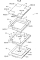
- Fig. 1 is a perspective view of the condenser microphone M
- Fig. 2 is a sectional view of the condenser microphone M taken along line II-II of Fig. 1 , and more particularly along a short axis of the condenser microphone M
- Fig. 3 is an exploded perspective view of the condenser microphone M seen from a top surface 1a of a casing body 1
- Fig. 4 is an exploded perspective view of the condenser microphone M seen from a bottom surface 1b of the casing body 1. As shown in Figs.
- the condenser microphone M in accordance with the present invention comprises the casing body 1 having an acoustic hole 15 formed in the top surface 1a, a capacitor section C including a diaphragm electrode 14, a fixed electrode 23 and an electret membrane 24 formed on the diaphragm electrode 14 or fixed electrode 23, a converting circuit section 45 for converting variations of the capacitance of the capacitor section C into electric signals for output, and a conductive section for making the capacitor section C electrically conductive with the converting circuit section 45.
- the capacitor section C, converting circuit section 45 and conductive section are mounted inside the casing body 1.
- the rectangular casing body 1 of the condenser microphone M includes a first layer 10 acting as a first rectangular plate member forming the top surface 1a of the casing body 1, a second layer 20 acting as a rectangular intermediate member, a third layer 30 also acting as a rectangular intermediate member, and a fourth layer 40 acting as a second rectangular plate member forming the bottom surface 1b of the casing body 1. While this embodiment gives an example where the intermediate member includes two layers, i.e. the second layer 20 and third layer 30, the intermediate member may include only one element or three or more.
- the electret membrane 24 may be provided on the diaphragm electrode 14.
- the first layer 10 includes the acoustic hole 15 and diaphragm electrode 14 of the condenser microphone M. More particularly, an insulating first base member 11 includes first conductive portions 12a and 18a, and a first insulating portion 13 mounted in the mentioned order on the side adjacent the top surface 1a. It should be noted that the first conductive portions 12a as shown are electrically conductive with each other while the first conductive portions 12a and the first conductive portion 18a are separated and electrically insulated from each other.
- the first base member 11 includes a first conductive portion 12b and the diaphragm electrode 14 laminated in the mentioned order on the side opposed to the bottom surface 1b, and a first conductive portion 18b formed on this side. It should be noted that the first conductive portion 12b and the diaphragm electrode 14 are electrically conductive with each other while the first conductive portion 12b and the first conductive portion 18b are separated and electrically insulated from each other.
- the first base member 11 includes the circular acoustic hole 15 formed therein.
- the surface of the first base member 11 remains annularly exposed around the acoustic hole 15 adjacent the top surface 1a.
- the first conductive portions 12a act as ground terminal element G and surface terminal element S
- the first conductive portion 18a acts as an output terminal element O and the surface terminal S of the condenser microphone M.
- Around the acoustic hole 15 is formed an annular exposed portion 17 to surround the exposed surface of the first base member 11.
- the first insulating portion 13 surrounds the exposed portion 17 noted above and covers parts of the first conductive portions 12a and the first conductive portion 18a.
- the first insulating portion 13 has a cross shape centering on the acoustic hole 15. Therefore, in the four corners of the top surface 1a of the casing body 1, the first conductive portions 12a are exposed at three corners while the first conductive portion 18a is exposed at one corner.
- the first conductive portion 12b formed peripherally of the first base member 11 on the side opposed to the bottom surface 1b acts as the ground terminal element G, and has a projection 12c protruding toward the side away from the first base member 11.
- the projection 12c has a rectangular flat portion at a distal end thereof to which the diaphragm electrode 14 having the same size as the projection is joined.
- the projection 12c has a circular aperture having the same diameter as the acoustic hole 15 in the side contacting the first base member 11 to allow sounds to enter the interior of the casing body 1 from the outside of the casing body 1 through the aperture.
- the projection 12c opens toward the bottom surface 1b to define a cylindrical space having an inner diameter larger than that of the aperture.
- the diaphragm electrode 14 is joined to the projection to cover the opening, using a conductive adhesive. Thus, the diaphragm electrode 14 can vibrate within the cylindrical space defined by the projection 12c.
- the second layer 20 includes the fixed electrode 23 and the electret membrane 24 arranged in a central portion of an insulating second base member 21 in the mentioned order to be opposed to the projection 12c and the diaphragm electrode 14.
- the second base member 21 includes, formed peripherally on the side adjacent the top surface 1a, a second conductive portion 22a for contacting the first conductive portion 12b, and a second conductive portion 28a for contacting the first conductive portion 18b.
- the first conductive portion 12b and the second conductive portion 22a are joined to each other, and the first conductive portion 18b and the second conductive portion 28a are joined to each other, by the conductive adhesive, respectively.
- the diaphragm electrode 14 of the first layer 10 and the fixed electrode 23 and the electret membrane 24 of the second layer 20 constitute the capacitor section C of the condenser microphone M of the present invention.
- the gap between the diaphragm electrode 14 and the electret membrane 24 is adjusted by the thickness of the first conductive portions 12b and 18b, the thickness of the second conductive portions 22a and 28a and the thickness of the conductive adhesive.
- a second conductive portion 22b is formed peripherally of the second base member 21 on the side adjacent the bottom surface 1b, while a second conductive portion 28b is formed in a position remote from the second conductive portion 22b to be electrically insulated from the second conductive portion 22b.
- the second conductive portions 22a and 22b act as the ground terminal element G while the second conducive portions 28a and 28b act as the output terminal element O.
- the third layer 30 includes an insulating third base member 31.
- the third base member 31 includes, formed on the side opposed to the top surface 1a, a third conductive portion 32a having the same shape as the second conductive portion 22b and contacting the second conductive portion 22b, and a third conductive portion 37a having the same shape as the second conductive portion 28b and contacting the second conductive portion 28b.
- the second conductive portion 22b and the third conductive portion 32a are joined to each other, and the second conductive portion 28b and the third conductive portion 37a are joined to each other, by the conductive adhesive, respectively.
- the third base member 31 includes, on the side adjacent the bottom surface 1b, a third conductive portion 32b formed peripherally thereof, and a third conductive portion 37b formed in a position remote from the third conductive portion 32b to be electrically insulated from the third conductive portion 32b.
- the third conductive portions 32a and 32b act as the ground terminal element G while the third conductive portions 37a and 37b act as the output terminal element O.
- the fourth layer 40 includes an insulating fourth base member 41.
- the fourth base member 41 includes, formed on the side opposed to the top surface 1a, a fourth conductive portion 42a having the same shape as the third conductive portion 32b and contacting the third conductive portion 32b, and a fourth conductive portion 47a having the same shape as the third conductive portion 37b and contacting the third conductive portion 37b.
- the third conductive portion 32b and the fourth conductive portion 42a are joined to each other, and the third conductive portion 37b and the fourth conductive portion 47a are joined to each other, by the conductive adhesive, respectively.
- the fourth conductive portion 42a is conductive with a circuit pattern of the converting circuit section 45 for converting variations of the capacitance of the capacitor section C to electric signals for output.
- Various elements such as an FET 44 forming part of the converting circuit section 45 are mounted on the circuit pattern.
- the fourth base member 41 includes, formed on the side adjacent the bottom surface 1b, fourth conductive portions 42b and 47b and a fourth insulating portion 43 which are formed in the mentioned order. It should be noted that the fourth conductive portions 42b and the fourth conductive portion 47b are separated and electrically insulated from each other.
- the fourth insulating portion 43 has a cross shape. Therefore, in the four corners of the bottom surface 1b of the casing body 1, the fourth conductive portions 42b are exposed at three corners while the fourth conductive portion 47b is exposed at one corner.
- the first layer 10, second layer 20, third layer 30 and fourth layer 40 include side surfaces 1c defining end surfaces perpendicular to a long axis of the casing body 1.
- the side surfaces 1c have conductive side surface terminals 16, 26, 36 and 46 acting as the ground terminal element G which are electrically conductive with each other, and side surface terminals 19, 29, 39 and 49 acting as the output terminal element O which are electrically conductive with each other.
- first conductive portions 12a, side surface terminal 16, first conductive portion 12b, second conductive portion 22a, side surface terminal 26, second conductive portion 22b, third conductive portion 32a, side surface terminal 36, third conductive portion 32b, fourth conductive portion 42a, side surface terminal 46 and fourth conductive portions 42b are electrically conductive with one another.
- the first conductive portions 12a, side surface terminals 16, 26, 36 and 46 and fourth conductive portions 42b exposed on the surfaces of the casing body 1 constitute the surface terminal element S (ground terminal element G) as a whole extending from the top surface 1a through the side surface 1c to the bottom surface 1b.
- the first conductive portion 18a, side surface terminal 19, first conductive portion 18b, second conductive portion 28a, side surface terminal 29, second conductive portion 28b, third conductive portion 37a, side surface terminal 39, third conductive portion 37b, fourth conductive portion 47a, side surface terminal 49 and fourth conductive portion 47b are electrically conductive with one another.
- the first conductive portion 18a, side surface terminals 19, 29, 39 and 49 and fourth conductive portion 47b exposed on the surface of the casing body 1 constitute the surface terminal element S (output terminal element 0) as a whole extending from the top surface 1a through the side surface 1c to the bottom surface 1b.
- the ground terminal element G and the output terminal element O are connected to the converting circuit section 45, respectively.
- the fixed electrode 23 provided in the second layer 20 includes a through hole 25 formed therein to contact a through hole 33 formed in the third layer 30.
- the through hole 33 in turn contacts the converting circuit section 45 provided on the fourth layer 40. Therefore, the fixed electrode 23 of the second layer 20 is electrically conductive with the FET 44.
- the diaphragm electrode 14 provided on the first layer 10 is electrically conductive with the FET 44 through the surface terminal element S noted above. In other words, the capacitor section C is electronically connected to the FET 44.
- the diaphragm electrode 14 is vibrated by sounds entering from the acoustic hole 15, and variations of the capacitance of the capacitor section C are transmitted to the converting circuit section 45 having the FET 44 to be converted into electric signals and outputted from the converting circuit section 45 to the output terminal element O.
- the through hole 33 formed in the third layer 30 acts as the conductive section for making the capacitor section C (the fixed electrode 23 and the electret membrane 24) electrically conductive with the converting circuit section 45.
- a plurality of through bores 27 are formed in the second base member 21 of the second layer 20.
- the space between the first layer 10 and the second layer 20 and the space between the second layer 20 and the fourth layer 40 communicate with each other through the plurality of through bores 27 extending from the second layer 20 toward the third layer 30.
- the air present in those spaces is able to circulate in response to vibrations of the diaphragm electrode 14.
- the provision of the plurality of through bores 27 improves the vibration property of the diaphragm electrode 14 to facilitate its vibration.
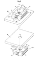
- Fig. 5(a) is an explanatory view showing a way of joining the casing body 1 of the condenser microphone M to a circuit board 50 at the bottom surface 1b.
- the condenser microphone M is jointed to the circuit board 50 by solder 52.
- the condenser microphone M in accordance with the present invention includes the surface terminal element S extending over the top surface 1a, the side surfaces 1c and the bottom surface 1b of the casing body 1, and thus a joining method can be employed in which a relatively large amount of solder 52 is provided on the side surfaces 1c of the casing body 1.
- the surface terminal element S includes two kinds of elements, the ground terminal element G and the output terminal element O.
- the ground terminal element G acting as the surface terminal element S provided on the top surface 1a, side surfaces 1c and bottom surface 1b of the casing body 1 also acts as an electromagnetic shield for the interior of the casing body 1.
- Fig. 5(b) is an explanatory view showing a way of joining the casing body 1 of the condenser microphone M to the circuit board 50 at the top surface 1a.
- a through bore 51 formed in the circuit board 50 is aligned with the acoustic hole 15 of the casing body 1 to allow the exposed portion 17 formed in the top surface 1a of the casing body 1 of the condenser microphone M to be joined to the circuit board 50 using the solder.
- the exposed portion 17 acts as a joint member. Therefore, no gap is produced between the region around the acoustic hole 15 of the casing body 1 and the circuit board 50.
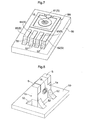
- Fig. 6(a) is a schematic sectional view showing a state where the condenser microphone M in accordance with the present invention is mounted on the circuit board 50
- Fig. 6(b) is a schematic sectional view showing a state where a conventional condenser microphone is mounted on the circuit board 50.
- solder 52 since a relatively large amount of solder 52 can be provided on the side surfaces 1c of the casing body 1, it is easy to remelt the solder 52 using a soldering iron 60 when the solder 52 is not mounted properly.
- the conventional condenser microphone has surface terminal elements 101 not provided on the side surfaces 1c, but provided only on the bottom surface 1b and the top surface 1a of a casing body 100.
- solder 52 contributing to the joint between the casing body 100 and the circuit board 50 is provided in positions difficult to visually recognize from outside.
- the solder 52 is provided in inward positions between the casing body 100 and the circuit board 50, and thus the soldering iron 60 does not easily reach the solder 52, which makes it difficult to remelt the solder 52.
Landscapes
- Engineering & Computer Science (AREA)
- Physics & Mathematics (AREA)
- Acoustics & Sound (AREA)
- Signal Processing (AREA)
- Manufacturing & Machinery (AREA)
- Electrostatic, Electromagnetic, Magneto- Strictive, And Variable-Resistance Transducers (AREA)
Applications Claiming Priority (1)
| Application Number | Priority Date | Filing Date | Title |
|---|---|---|---|
| JP2007166410A JP2009005253A (ja) | 2007-06-25 | 2007-06-25 | コンデンサマイクロホン |
Publications (1)
| Publication Number | Publication Date |
|---|---|
| EP2009952A2 true EP2009952A2 (de) | 2008-12-31 |
Family
ID=39776405
Family Applications (1)
| Application Number | Title | Priority Date | Filing Date |
|---|---|---|---|
| EP08011489A Withdrawn EP2009952A2 (de) | 2007-06-25 | 2008-06-24 | Kondensatormikrofon |
Country Status (6)
| Country | Link |
|---|---|
| US (1) | US20090003631A1 (de) |
| EP (1) | EP2009952A2 (de) |
| JP (1) | JP2009005253A (de) |
| KR (1) | KR20080114532A (de) |
| CN (1) | CN101336010A (de) |
| TW (1) | TW200908772A (de) |
Families Citing this family (1)
| Publication number | Priority date | Publication date | Assignee | Title |
|---|---|---|---|---|
| DE102011004589B4 (de) * | 2011-02-23 | 2013-02-07 | Siemens Aktiengesellschaft | Röntgendetektor, aufweisend eine Vielzahl von Sensorelementen |
Citations (1)
| Publication number | Priority date | Publication date | Assignee | Title |
|---|---|---|---|---|
| JP2007081614A (ja) | 2005-09-13 | 2007-03-29 | Star Micronics Co Ltd | コンデンサマイクロホン |
Family Cites Families (11)
| Publication number | Priority date | Publication date | Assignee | Title |
|---|---|---|---|---|
| JP3139139B2 (ja) * | 1992-06-05 | 2001-02-26 | 株式会社村田製作所 | チップ形圧電共振子およびその製造方法 |
| JP4093327B2 (ja) * | 1997-09-26 | 2008-06-04 | Tdk株式会社 | 高周波部品およびその製造方法 |
| JP2000050393A (ja) * | 1998-05-25 | 2000-02-18 | Hosiden Corp | エレクトレットコンデンサマイクロホン |
| JP3472493B2 (ja) * | 1998-11-30 | 2003-12-02 | ホシデン株式会社 | 半導体エレクトレットコンデンサーマイクロホン |
| JP4528461B2 (ja) * | 2001-05-16 | 2010-08-18 | シチズン電子株式会社 | エレクトレットコンデンサマイクロフォン |
| US7136500B2 (en) * | 2003-08-05 | 2006-11-14 | Knowles Electronics, Llc. | Electret condenser microphone |
| JP4188325B2 (ja) * | 2005-02-09 | 2008-11-26 | ホシデン株式会社 | 防塵板内蔵マイクロホン |
| JP2006238203A (ja) * | 2005-02-25 | 2006-09-07 | Hosiden Corp | マイクロホン |
| JP4150407B2 (ja) * | 2005-06-20 | 2008-09-17 | ホシデン株式会社 | 電気音響変換器 |
| JP2007043327A (ja) * | 2005-08-01 | 2007-02-15 | Star Micronics Co Ltd | コンデンサマイクロホン |
| JP2007150647A (ja) * | 2005-11-28 | 2007-06-14 | Citizen Electronics Co Ltd | 小型マイクロホン |
-
2007
- 2007-06-25 JP JP2007166410A patent/JP2009005253A/ja active Pending
-
2008
- 2008-05-23 TW TW097119257A patent/TW200908772A/zh unknown
- 2008-06-20 US US12/143,212 patent/US20090003631A1/en not_active Abandoned
- 2008-06-20 KR KR1020080058318A patent/KR20080114532A/ko not_active Ceased
- 2008-06-24 EP EP08011489A patent/EP2009952A2/de not_active Withdrawn
- 2008-06-24 CN CNA2008101446353A patent/CN101336010A/zh active Pending
Patent Citations (1)
| Publication number | Priority date | Publication date | Assignee | Title |
|---|---|---|---|---|
| JP2007081614A (ja) | 2005-09-13 | 2007-03-29 | Star Micronics Co Ltd | コンデンサマイクロホン |
Also Published As
| Publication number | Publication date |
|---|---|
| JP2009005253A (ja) | 2009-01-08 |
| CN101336010A (zh) | 2008-12-31 |
| TW200908772A (en) | 2009-02-16 |
| KR20080114532A (ko) | 2008-12-31 |
| US20090003631A1 (en) | 2009-01-01 |
Similar Documents
| Publication | Publication Date | Title |
|---|---|---|
| TWI376963B (de) | ||
| JP4751057B2 (ja) | コンデンサマイクロホンとその製造方法 | |
| EP1755360B1 (de) | Silizium Kondensatormikrofon und Verfahren zum Einbringen eines Mikrofons in ein Gehäuse | |
| JP2007081614A (ja) | コンデンサマイクロホン | |
| JP2009071346A (ja) | コンデンサマイクロホン | |
| JP2003259494A (ja) | エレクトレットコンデンサマイクロホン | |
| JP3974918B2 (ja) | コンデンサーマイクロホン | |
| EP0499237B1 (de) | Elektret Kondensator Mikrofon und Verfahren zu dessen Herstellung | |
| JP2003153392A (ja) | エレクトレットコンデンサマイクロホン | |
| US20090274324A1 (en) | Microphone unit and method of manufacturing the same | |
| CN101002503B (zh) | 电容传声器 | |
| JP5097603B2 (ja) | マイクロホンユニット | |
| JP2007201383A (ja) | 蓄電デバイス | |
| EP2009952A2 (de) | Kondensatormikrofon | |
| WO2007032581A1 (en) | Silicon based condenser microphone | |
| JP2003259493A (ja) | エレクトレットコンデンサマイクロホン | |
| EP1699258B1 (de) | Elektro-akustischer Wandler mit Halterung | |
| CN101427594B (zh) | 驻极体电容传声器 | |
| KR101731039B1 (ko) | 마이크로폰 패키지 | |
| KR100797438B1 (ko) | 커링공정이 필요없는 마이크로폰 및 그 조립방법 | |
| JP2006238203A (ja) | マイクロホン | |
| JP6555960B2 (ja) | 電子部品搭載用パッケージおよび電子装置 | |
| KR200435142Y1 (ko) | 콘덴서 마이크로폰 전극 연결구조 | |
| CN1961610B (zh) | 平行六面体型方向性电容式传声器 |
Legal Events
| Date | Code | Title | Description |
|---|---|---|---|
| PUAI | Public reference made under article 153(3) epc to a published international application that has entered the european phase |
Free format text: ORIGINAL CODE: 0009012 |
|
| AK | Designated contracting states |
Kind code of ref document: A2 Designated state(s): AT BE BG CH CY CZ DE DK EE ES FI FR GB GR HR HU IE IS IT LI LT LU LV MC MT NL NO PL PT RO SE SI SK TR |
|
| AX | Request for extension of the european patent |
Extension state: AL BA MK RS |
|
| STAA | Information on the status of an ep patent application or granted ep patent |
Free format text: STATUS: THE APPLICATION HAS BEEN WITHDRAWN |
|
| 18W | Application withdrawn |
Effective date: 20110428 |