EP2010323B1 - Verfahren und vorrichtung zur elektrokinetischen handhabung - Google Patents
Verfahren und vorrichtung zur elektrokinetischen handhabung Download PDFInfo
- Publication number
- EP2010323B1 EP2010323B1 EP07736200A EP07736200A EP2010323B1 EP 2010323 B1 EP2010323 B1 EP 2010323B1 EP 07736200 A EP07736200 A EP 07736200A EP 07736200 A EP07736200 A EP 07736200A EP 2010323 B1 EP2010323 B1 EP 2010323B1
- Authority
- EP
- European Patent Office
- Prior art keywords
- electrodes
- electrode
- electrically
- floating
- electrode structures
- Prior art date
- Legal status (The legal status is an assumption and is not a legal conclusion. Google has not performed a legal analysis and makes no representation as to the accuracy of the status listed.)
- Not-in-force
Links
Images


Classifications
-
- B—PERFORMING OPERATIONS; TRANSPORTING
- B01—PHYSICAL OR CHEMICAL PROCESSES OR APPARATUS IN GENERAL
- B01L—CHEMICAL OR PHYSICAL LABORATORY APPARATUS FOR GENERAL USE
- B01L3/00—Containers or dishes for laboratory use, e.g. laboratory glassware; Droppers
- B01L3/50—Containers for the purpose of retaining a material to be analysed, e.g. test tubes
- B01L3/502—Containers for the purpose of retaining a material to be analysed, e.g. test tubes with fluid transport, e.g. in multi-compartment structures
- B01L3/5027—Containers for the purpose of retaining a material to be analysed, e.g. test tubes with fluid transport, e.g. in multi-compartment structures by integrated microfluidic structures, i.e. dimensions of channels and chambers are such that surface tension forces are important, e.g. lab-on-a-chip
- B01L3/502761—Containers for the purpose of retaining a material to be analysed, e.g. test tubes with fluid transport, e.g. in multi-compartment structures by integrated microfluidic structures, i.e. dimensions of channels and chambers are such that surface tension forces are important, e.g. lab-on-a-chip specially adapted for handling suspended solids or molecules independently from the bulk fluid flow, e.g. for trapping or sorting beads or physically stretching molecules
-
- B—PERFORMING OPERATIONS; TRANSPORTING
- B01—PHYSICAL OR CHEMICAL PROCESSES OR APPARATUS IN GENERAL
- B01F—MIXING, e.g. DISSOLVING, EMULSIFYING OR DISPERSING
- B01F33/00—Other mixers; Mixing plants; Combinations of mixers
- B01F33/30—Micromixers
- B01F33/3031—Micromixers using electro-hydrodynamic [EHD] or electro-kinetic [EKI] phenomena to mix or move the fluids
-
- B—PERFORMING OPERATIONS; TRANSPORTING
- B03—SEPARATION OF SOLID MATERIALS USING LIQUIDS OR USING PNEUMATIC TABLES OR JIGS; MAGNETIC OR ELECTROSTATIC SEPARATION OF SOLID MATERIALS FROM SOLID MATERIALS OR FLUIDS; SEPARATION BY HIGH-VOLTAGE ELECTRIC FIELDS
- B03C—MAGNETIC OR ELECTROSTATIC SEPARATION OF SOLID MATERIALS FROM SOLID MATERIALS OR FLUIDS; SEPARATION BY HIGH-VOLTAGE ELECTRIC FIELDS
- B03C5/00—Separating dispersed particles from liquids by electrostatic effect
- B03C5/02—Separators
- B03C5/022—Non-uniform field separators
- B03C5/026—Non-uniform field separators using open-gradient differential dielectric separation, i.e. using electrodes of special shapes for non-uniform field creation, e.g. Fluid Integrated Circuit [FIC]
-
- B—PERFORMING OPERATIONS; TRANSPORTING
- B03—SEPARATION OF SOLID MATERIALS USING LIQUIDS OR USING PNEUMATIC TABLES OR JIGS; MAGNETIC OR ELECTROSTATIC SEPARATION OF SOLID MATERIALS FROM SOLID MATERIALS OR FLUIDS; SEPARATION BY HIGH-VOLTAGE ELECTRIC FIELDS
- B03C—MAGNETIC OR ELECTROSTATIC SEPARATION OF SOLID MATERIALS FROM SOLID MATERIALS OR FLUIDS; SEPARATION BY HIGH-VOLTAGE ELECTRIC FIELDS
- B03C5/00—Separating dispersed particles from liquids by electrostatic effect
- B03C5/02—Separators
- B03C5/022—Non-uniform field separators
- B03C5/028—Non-uniform field separators using travelling electric fields, i.e. travelling wave dielectrophoresis [TWD]
-
- C—CHEMISTRY; METALLURGY
- C12—BIOCHEMISTRY; BEER; SPIRITS; WINE; VINEGAR; MICROBIOLOGY; ENZYMOLOGY; MUTATION OR GENETIC ENGINEERING
- C12M—APPARATUS FOR ENZYMOLOGY OR MICROBIOLOGY; APPARATUS FOR CULTURING MICROORGANISMS FOR PRODUCING BIOMASS, FOR GROWING CELLS OR FOR OBTAINING FERMENTATION OR METABOLIC PRODUCTS, i.e. BIOREACTORS OR FERMENTERS
- C12M47/00—Means for after-treatment of the produced biomass or of the fermentation or metabolic products, e.g. storage of biomass
- C12M47/04—Cell isolation or sorting
-
- B—PERFORMING OPERATIONS; TRANSPORTING
- B01—PHYSICAL OR CHEMICAL PROCESSES OR APPARATUS IN GENERAL
- B01L—CHEMICAL OR PHYSICAL LABORATORY APPARATUS FOR GENERAL USE
- B01L2200/00—Solutions for specific problems relating to chemical or physical laboratory apparatus
- B01L2200/06—Fluid handling related problems
- B01L2200/0647—Handling flowable solids, e.g. microscopic beads, cells, particles
-
- B—PERFORMING OPERATIONS; TRANSPORTING
- B01—PHYSICAL OR CHEMICAL PROCESSES OR APPARATUS IN GENERAL
- B01L—CHEMICAL OR PHYSICAL LABORATORY APPARATUS FOR GENERAL USE
- B01L2200/00—Solutions for specific problems relating to chemical or physical laboratory apparatus
- B01L2200/12—Specific details about manufacturing devices
-
- B—PERFORMING OPERATIONS; TRANSPORTING
- B01—PHYSICAL OR CHEMICAL PROCESSES OR APPARATUS IN GENERAL
- B01L—CHEMICAL OR PHYSICAL LABORATORY APPARATUS FOR GENERAL USE
- B01L2300/00—Additional constructional details
- B01L2300/06—Auxiliary integrated devices, integrated components
- B01L2300/0627—Sensor or part of a sensor is integrated
- B01L2300/0636—Integrated biosensor, microarrays
-
- B—PERFORMING OPERATIONS; TRANSPORTING
- B01—PHYSICAL OR CHEMICAL PROCESSES OR APPARATUS IN GENERAL
- B01L—CHEMICAL OR PHYSICAL LABORATORY APPARATUS FOR GENERAL USE
- B01L2300/00—Additional constructional details
- B01L2300/08—Geometry, shape and general structure
- B01L2300/0809—Geometry, shape and general structure rectangular shaped
- B01L2300/0819—Microarrays; Biochips
-
- B—PERFORMING OPERATIONS; TRANSPORTING
- B01—PHYSICAL OR CHEMICAL PROCESSES OR APPARATUS IN GENERAL
- B01L—CHEMICAL OR PHYSICAL LABORATORY APPARATUS FOR GENERAL USE
- B01L2300/00—Additional constructional details
- B01L2300/08—Geometry, shape and general structure
- B01L2300/0861—Configuration of multiple channels and/or chambers in a single devices
- B01L2300/0877—Flow chambers
-
- B—PERFORMING OPERATIONS; TRANSPORTING
- B01—PHYSICAL OR CHEMICAL PROCESSES OR APPARATUS IN GENERAL
- B01L—CHEMICAL OR PHYSICAL LABORATORY APPARATUS FOR GENERAL USE
- B01L2400/00—Moving or stopping fluids
- B01L2400/04—Moving fluids with specific forces or mechanical means
- B01L2400/0403—Moving fluids with specific forces or mechanical means specific forces
- B01L2400/0415—Moving fluids with specific forces or mechanical means specific forces electrical forces, e.g. electrokinetic
- B01L2400/0424—Dielectrophoretic forces
-
- B—PERFORMING OPERATIONS; TRANSPORTING
- B01—PHYSICAL OR CHEMICAL PROCESSES OR APPARATUS IN GENERAL
- B01L—CHEMICAL OR PHYSICAL LABORATORY APPARATUS FOR GENERAL USE
- B01L2400/00—Moving or stopping fluids
- B01L2400/04—Moving fluids with specific forces or mechanical means
- B01L2400/0493—Specific techniques used
- B01L2400/0496—Travelling waves, e.g. in combination with electrical or acoustic forces
-
- B—PERFORMING OPERATIONS; TRANSPORTING
- B01—PHYSICAL OR CHEMICAL PROCESSES OR APPARATUS IN GENERAL
- B01L—CHEMICAL OR PHYSICAL LABORATORY APPARATUS FOR GENERAL USE
- B01L3/00—Containers or dishes for laboratory use, e.g. laboratory glassware; Droppers
- B01L3/50—Containers for the purpose of retaining a material to be analysed, e.g. test tubes
- B01L3/502—Containers for the purpose of retaining a material to be analysed, e.g. test tubes with fluid transport, e.g. in multi-compartment structures
- B01L3/5027—Containers for the purpose of retaining a material to be analysed, e.g. test tubes with fluid transport, e.g. in multi-compartment structures by integrated microfluidic structures, i.e. dimensions of channels and chambers are such that surface tension forces are important, e.g. lab-on-a-chip
- B01L3/502738—Containers for the purpose of retaining a material to be analysed, e.g. test tubes with fluid transport, e.g. in multi-compartment structures by integrated microfluidic structures, i.e. dimensions of channels and chambers are such that surface tension forces are important, e.g. lab-on-a-chip characterised by integrated valves
Definitions
- the present invention relates to object manipulation and, more particularly, to a method and device for manipulating small scale objects by electrokinetics.
- Electrokinetics is the use of electrical fields (and the resulting forces) to manipulate matter in a fluid medium. Electrokinetics is a term which encompasses all types of processes in which the application of electric field results in motion of matter.
- Electrophoresis is a phenomenon in which charged particles, located between two electrically biased electrodes, are influenced by the electric field generated by the electrodes such that they are attracted to one electrode and repulsed by the other electrode. The attracting and repulsing forces are proportional to the particle net charge and the electric field magnitude.
- Dielectrophoresis is the motion of matter caused by polarization effects in a nonuniform electric field. Electric fields induce dielectric polarization components in polarizable particles. The extent of the particle's polarization is related to its effective dielectric constant (polarizability) and to the electric field magnitude. Particles that have high dielectric constants experience significant polarization while particles that have low dielectric constants experience lower polarization.
- particle motion is produced by the interaction between the nonuniform electric field and the dielectric polarization components induced in the particle and in the surrounding fluid medium by the field. In a uniform field, neutral particles, including neutral polarized particles, experience no net electric force.
- the principle of dielectrophoresis has become a popular technique for separating objects such as biological cells or microparticles in suspension.
- the ability to identify, characterize and purify cell subpopulations is fundamental to numerous biological and medical applications, often forming the starting point for research protocols and the basis for current and emerging clinical protocols.
- Cell separation has numerous applications in medicine, biotechnology and environmental study. For example, cell separation can make possible life-saving procedures such as autologous bone marrow transplantation for the remediation of advanced cancers in which the removal of cancer-causing metastatic cells from a patient's marrow is necessary. In other applications, such as the study of signaling between blood cells, highly purified cell subpopulations permit studies that would otherwise be impossible.
- a key advantage of dielectrophoretic separation over currently used separation techniques is that dielectrophoresis effectively maps biophysical properties into electrostatic forces whose direction and magnitude reflect cellular properties.
- the analysis of the dielectrophoretic motion of cells thus permits biophysical parameters, such as capacitance and surface conductance, to be probed.
- Dielectrophoretic forces are generated by either conventional dielectrophoresis (cDEP, also termed classic dielectrophoresis or simply dielectrophoresis) or by traveling-wave dielectrophoresis (twDEP).
- Classic dielectrophoresis refers to motion arising from nonuniform distribution in the magnitude of a direct-current (DC) or alternating-current (AC) electric field.
- Traveling-wave dielectrophoresis refers to motion arising from nonuniform distribution in the phase of an alternating-current electric field.
- nonuniform electric fields required for the implementation of dielectrophoresis are typically generated by microelectrodes connected via electrical contacts to an AC or DC power source.
- Known in the art are two major techniques for generating nonuniform electric fields.
- the electrodes are arranged in a specialized geometry such as a castellated arrangement [ Green, N. G., Morgan, H., J. Phys. D 1998, 31, L25-L30 ; and Morgan, H., Hughes, M. P., Green, N. G., Biophys. J. 1999, 77, 516-525 ].
- These geometries are characterized by a variable distance between the electrodes, such that the electric field is higher in regions in which the electrodes are closer and lower in regions in which the electrodes are farther apart. This results in nonuniform electric fields.
- the electrodes are arranged in a symmetric geometry, and the motion of particles is achieved by subjecting them to a specific voltage [ Li, H., Bashir, R., Sensors aszd Actuators 2002, 86, 215-221 ; Talary, M. S., Burt, J. P. H., Tame, J. A., Pethig, R., J. Phys. D 1996, 29, 2198-2203 ; Xu, J. Q. , Wu, L., Huang, M., Yang, W., Cheng, J., Wang, X., in: Micro Total Analysis Systems, Monterey 2001, pp.
- the applied voltage is in the form of a pulse sequence, which is typically characterized by constant amplitude and half-cycle or quarter-cycle phase sequence.
- the operation of devices employing a half-cycle phase sequence is based on classic dielectrophoresis and the dielectrophoretic force produced thereby is perpendicular to the electrode plane.
- the operation of devices employing a quarter-cycle phase sequence is based on traveling wave dielectrophoresis and the dielectrophoretic force produced thereby is parallel to the electrode plane.
- a device for manipulating an object present in a fluid by electrokinetics as defined in claim 1.
- the electrically floating electrode structure(s) is designed and configured to control non-uniformities in the electric field.
- the electrically floating electrode structure(s) is designed and configured to increase non-uniformities in the electric field.
- a method of fabricating a device for manipulating an object by electrokinetics comprises: fabricating a plurality of electrode structures in a chamber; fabricating a plurality of electrical contacts in the chamber; and connecting a portion of the plurality of electrode structures to the plurality of electrical contacts, so as to provide a plurality of electrically biasable electrode structures while maintaining and at least one electrically floating electrode structure, the electrically floating electrode structure(s) being designed and configured to increase non-uniformities in an electric field generated upon activation of the plurality of electrically biasable electrode structures.
- At least one of the plurality of electrically biasable electrode structures is characterized by at least one nanometric dimension. According to still further features in the described preferred embodiments the electrically biasable electrode structures are characterized by at least one micrometric dimension.
- the electrically floating electrode structure(s) is designed and constructed to increase a dielectrophoretic force exerted on the object by at least one, more preferably at least two, more preferably at least three orders of magnitude. According to still further features in the described preferred embodiments at least one electrically floating electrode structure is designed and constructed to increase a dielectrophoretic force exerted on the object by more than three orders of magnitude.
- the electrically biasable electrode structures comprise interdigitated electrodes.
- the electrically floating electrode structures comprise carbon nanotubes.
- the device or apparatus further comprises a power source device, electrically connected to the plurality of electrically biasable electrode structures and configured for applying bias thereto.
- the power source device is configured to provide out-of-phase signals to individual members of the plurality of electrodes.
- the out-of-phase signals are selected such as to generate a traveling wave dielectrophoretic force.
- the out-of-phase signals are selected such as to generate a classical dielectrophoretic force.
- the power source device is a direct-current power source device.
- device or apparatus further comprises a detector for detecting the presence of the object.
- the detector is designed and constructed for detecting variations in the electrical characteristics in a predetermined region within the chamber.
- the detector is designed and constructed for detecting variations in the optical characteristics in a predetermined region within the chamber.
- the device or apparatus further comprises at least one inlet port and at least one outlet port, the at least one inlet port and the at least one outlet port being in fluid communication with the chamber, and a fluid flow system for supplying the fluid to the at least one inlet port and removing the fluid from at least one outlet.
- the object is made of organic material.
- the object is made of non-organic material.
- the object comprises a biological molecule.
- the object comprises a non-biological molecule.
- the fluid is a biological fluid.
- the fluid is a non-biological fluid.
- the object is selected from the group consisting of a cell, cell aggregate, cell organelle, nucleic acid, bacterium, protozoan and virus.
- the object is an aggregate of inorganic matter.
- the object is an organic material, isomer thereof or isotope thereof.
- the object is suspended inorganic matter.
- the object is dissolved inorganic matter.
- the present invention successfully addresses the shortcomings of the presently known configurations by providing a device, apparatus and method for manipulating an object by electrokinetics.
- Implementation of the present invention involves performing or completing selected tasks or steps manually, automatically, or a combination thereof.
- several selected steps could be implemented by hardware or by software on any operating system of any firmware or a combination thereof.
- selected steps of the invention could be implemented as a chip or a circuit.
- selected steps of the invention could be implemented as a plurality of software instructions being executed by a computer using any suitable operating system.
- selected steps of the method and system of the invention could be described as being performed by a data processor, such as a computing platform for executing a plurality of instructions.
- the present embodiments comprise a device and method which can be used to manipulate objects by electrokinetics. Specifically, but not exclusively, the present embodiments can be used to manipulate small scale objects by dielectrophoresis.
- the present embodiments further comprise a method suitable for manufacturing a device for manipulating an object.
- the device and method of the present embodiments can therefore be used to manipulate electrically neutral as well as charged objects, which can be conductive, dielectric or semiconductive.
- the manipulated objects can be made of any material, including, without limitation, inorganic material e.g ., minerals, crystals, colloidal and gas bubbles, organic material or biological material e.g ., cells, nucleic acids, bacteria, protozoans and viruses.
- the manipulated objects can also be in the form of cell aggregates, cell organelles, molecules or molecular aggregates, such as, but not limited to, proteins and nucleic acids.
- the objects are typically present in a fluid, such as, but not limited to, water, a biological fluid (for example, body fluid, e.g ., blood, plasma, urine, saliva, vaginal secretions, feces and wound excrement), a bacterial cell suspension, a protein medium, an antibody medium, a nucleic acid medium, ink and the like and fluid media commonly used in standard medical applications such as phosphate buffered saline.
- the fluid may include more than one type of objects, such as, but not limited to, a mixture of cell types.
- the device and method manipulate the objects by applying forces so as to change their kinematical properties.
- the device and method of the present embodiments can be used to discriminate between distinctive types of objects because the analysis of the kinematical properties of the manipulated objects (position, velocity, acceleration) allows to identify their various characteristics or at least to separate the objects according to their different kinematical properties.
- the present embodiments can be used to manipulate erythrocytes in a blood sample, abnormal erythrocytes (e.g ., erythrocyte infested with malaria) in a blood sample containing normal and abnormal erythrocytes, fetal nucleated red blood cells in a mixture of maternal blood, cancer cells in a mixture with normal cells.
- abnormal erythrocytes e.g ., erythrocyte infested with malaria
- fetal nucleated red blood cells in a mixture of maternal blood
- cancer cells in a mixture with normal cells.
- the present embodiments are useful to manipulated objects of any size.
- the present embodiments are useful for particles in the sub-millimeter scale.
- a characteristic length scale for the manipulated particles can therefore be from about 1 nm to about 500 ⁇ m, more preferably from about 10 nm to about 50 ⁇ m, more preferably from about 10 nm to about 1 ⁇ m.
- Small size particles can be, for example, chemical or biological molecules (including proteins, DNA, RNA, antibodies, antigens and lipids), assemblages of molecules, viruses, plasmids, bacteria, cells or cell aggregates, protozoans, embryos or other small organisms, as well as non-biological molecules, assemblages thereof, minerals, crystals, colloidal, conductive, semiconductive or dielectric particles and gas bubbles.
- chemical or biological molecules including proteins, DNA, RNA, antibodies, antigens and lipids
- assemblages of molecules viruses, plasmids, bacteria, cells or cell aggregates, protozoans, embryos or other small organisms, as well as non-biological molecules, assemblages thereof, minerals, crystals, colloidal, conductive, semiconductive or dielectric particles and gas bubbles.
- the device and method of the present embodiments are capable of separating cells without the need to alter them with ligands, stains, antibodies or other means. Cells remain undamaged, unaltered and viable during and following separation. Non-biological applications similarly require no such alteration. It is to be understood, however, that the device and method of the present embodiments are also suitable for separating the objects even if they have been so altered.
- Figure 1 illustrates a device 10 for manipulating an object present in a fluid.
- Device 10 comprises a substrate 12 forming a flow chamber shown generally at 14 .
- Device 10 further comprises a plurality of electrically biasable electrode structures 16 and one or more electrically floating electrode structures 18 . Electrode structures 16 and 18 are formed on or integrated with substrate 12 .
- floating electrode structure refers to an electrode structure that is separated from a conductive or semiconductive body by an intervening dielectric having thickness and other properties selected to substantially prevent flow of charge carriers to the electrode structure.
- biasable electrode structure refers to an electrode structure that is configured to be electrically connected to a power source, e.g., via a contact pad or the like, in a manner such that upon activation of the power source, charge carriers flow from the power source to the electrode structure or from the electrode structure to the power source, and the electrode structure becomes electrically biased.
- device 10 comprises an additional substrate 20 , spaced apart from substrate 12 such that flow chamber 14 is defined between substrates 12 and 20 .
- substrates 12 and 20 can be planar substrates engaging different planes and flow chamber 14 can be defined in the volume between the two different planes.
- Shown in Figure 1 is a six electrode structure configuration with six parallel electrode structures such that the two outermost structures are floating electrode structures, the two next-to-outermost structures are biasable electrode structures and the two innermost structures are floating electrode structures positioned between the biasable electrode structures
- device 10 can comprise any number of electrode structures in any orientation, provided there is at least one floating electrode structure and at least two biasable electrode structures.
- device 10 comprises a pair of biasable electrode structures and a single floating electrode structure.
- the floating electrode is preferably, but not obligatorily, positioned between the biasable electrodes.
- electrode structure applies also to a plurality of electrode structures and vice versa.
- Substrates 12 and 20 are made of electrically insulating or dielectric material which is preferably, but not obligatorily transparent to visible light to allow monitoring locomotion of objects within the device by visual or other optical means.
- materials suitable for substrate 12 and 20 include, without limitation, glass, silicon dioxide, resistive (non-conductive) silicon, plastics (such as, but not limited to, those used for printed circuit board substrates), elastomers (e.g ., poly-dimethylsiloxane), insulating photoresists (e.g ., SU-8) ceramic or the like.
- the electrode structures of device 10 can be made of any electrically conductive material such as, but not limited to, evaporated metal layers, conductive polymers, photoelectric materials or the like.
- the electrode structures may be in direct contact with the fluid or fluids, or they may be separated from them by a thin passivation layer or layers (e.g ., a film of SiO 2 , a photoresist, an elastomer, an adhesive, silicon nitride or a biologically selective and functional layer).
- the floating electrode structure of device 10 is designed and configured to increase and/or control nonuniformities in the electric field generated upon application of bias to the electrically biasable electrode structures.
- the floating electrode is designed and configured to provide a predetermined nonuniform electric field distribution in chamber 14.
- the control and/or increment of the electric field non-uniformity can be done by selecting the number, shape, size, material and/or position of the floating electrode structure.
- Nonuniform electric field is particularly useful when it is desired to use device 10 for manipulating neutral objects. In this case, the nonuniform electric field exerts dielectrophoretic forces on the objects.
- the floating electrode structure can significantly increase the dielectrophoretic force exerted on the object.
- the floating electrode structure is designed and constructed to increase the dielectrophoretic force by at least one, more preferably at least two most preferably at least three orders of magnitude. In other embodiments, the dielectrophoretic force is increased by more than three orders of magnitude. Since in operation there is no bias which is applied to the floating electrode structure, the increment of the dielectrophoretic force, via the field intensity gradients, is achieved without increasing the applied bias and/or substantially increasing the electric field.
- the amount by which the floating electrode structure increases the nonuniformity of the electric field in the device can be obtained experimentally, by analytic calculations and/or by numeric simulations.
- device 10 and another device similar to device 10 but with no floating electrode structure (or with the floating electrode structure replaced by a biasable electrode structure), can be manufactured and connected to a power source so as to generate electric field.
- Nonuniformities in the electric fields within the two devices can then be measured and compared to ensure that the floating electrode structure increases nonuniformities.
- the effect of the floating electrode structure can be determined by numerical simulation or theoretical analysis.
- the nonuniformity in the electric field for two similar devices, with and without floating electrode structure can be calculated or numerically simulated and compared to ensure that the floating electrode structure increases nonuniformities.
- the biasable and floating electrode structures can be of any size and shape. In one embodiment, the biasable and floating electrode structures are characterized by one or more micrometric dimensions.
- the biasable and floating electrode structures can be linear electrodes having a width of from about 5 ⁇ m to about 150 ⁇ m, a length of from about 100 ⁇ m to about 2.5 mm and a thickness of from about 10 nm to about 1 ⁇ m.
- the biasable electrode structures are characterized by one or more micrometric dimensions
- the floating electrode structures are characterized by one or more nanometric dimensions.
- the biasable electrode structures can be of the shape and size described above and the floating electrode structure can be, or it can be formed of nanostructures, such as, but not limited to, carbon nanotubes, e.g. , fullerene carbon nanotubes which can be, either single-walled or multi walled nanotubes.
- This embodiment combines the advantage of micrometric biasable electrode structures from the standpoint of relatively simple manufacturing process with the advantage of nanometric floating electrode structures from the standpoint of relatively large obtainable non-uniformities in the electric field. For example, non-uniformities obtainable using a device having two linear micrometric electrode structures and two linear nanometric electrode structures are larger by approximately three orders of magnitude in comparison with nonuniformities obtainable using a device having four linear micrometric electrode structures.
- biasable electrode structures are characterized by one or more nanometric dimensions.
- the electrically biasable electrode structures can be of any shape and can be arranged in any geometrical configuration.
- the electrically biasable electrode structures can be interdigitated electrodes.
- interdigitated means that a plurality of "digits" of a first electrode group is disposed alternately with a plurality of "digits" of a second electrode group.
- the geometry, dimensions and overall shape of the interdigitated electrodes may vary in different embodiments.
- a particular advantage of device 10 is the use of floating electrode structure, since device 10 generally includes fewer connections to external signal sources.
- the reduced number of connections allows miniaturization and improves conventional devices at least from the standpoint of compactness, since external signal connections tend to be bulky.
- the dielectroplioretic force is proportional to the volume of the manipulated object.
- the dielectrophoretic forces experienced by small objects are significantly lower than the dielectrophoretic forces experienced by larger objects.
- the dielectrophoretic forces experienced by nanoparticles are about 10 9 times weaker than the dielectrophoretic forces experienced by microparticles.
- One traditional approach for manipulating nanoparticles by dielectrophoresis calls for increasing the voltages applied to the electrodes.
- Function generators capable of producing such high voltages are rarely, if at all, attainable.
- working with too high voltages can be hazardous.
- Another traditional approach calls for the fabrication of electrodes having much smaller feature sizes and much smaller inter-electrode separation.
- nano-electrodes may have to be fabricated. Such fabrication is known to be difficult, in particular when all the electrodes are connected to external signal sources. The device of the present embodiments successfully overcomes these difficulties because the floating electrodes do not require external signal sources.
- An additional improvement presented by the device of the present embodiments is the aforementioned combination of biasable microelectrode structures and floating nanoelectrode structures.
- the increased dielectrophoretic force in the vicinity of a floating nanoelectrode structure of the present embodiments originates from imposing nanoscale changes on the potential distribution in these areas.
- the floating nanoelectrode structures do not considerably affect the potential and the electric field values, they significantly increase the field intensity gradients. This can be explained as follows: in the vicinity of a generally cylindrical floating electrode structure, the electric field intensity does not depend on the radius of the electrode structure, but the gradient of the electric field is inversely proportional to this radius.
- the gradient in the vicinity of a nanoelectrode structure is therefore about three orders of magnitude higher than in the vicinity of a microelectrode structure.
- the electric field gradient near the floating electrode structures is significantly higher than near the biasable electrode structures.
- An additional advantage of the technique of the present embodiments is the ability to provide high field gradients at many geometrical configurations of the biasable electrodes. This is because the high field gradients are local (near the floating electrodes) and it is not necessary to generate high field gradients near the biasable electrodes.
- the device of the present embodiments can comprise geometrical configurations other than polynomial.
- the device of the present embodiments can manipulate nanoparticles using, but not limited to, interdigitated biasable electrode structures and/or deflection electrodes and/or castellated electrodes and/or spiral electrodes and/or sinusoidal electrodes.
- An additional advantage of the technique of the present embodiments is the ability to increase the density of electrodes in the device by providing more floating electrode structures. Such configuration facilitates the simultaneous manipulation of many particles and offers a higher throughput.
- the floating electrode structure is of nanometric scale and the biasable electrode structures as well as the gap between adjacent biasable electrode structures are of micrometric scale, a single gap between adjacent biasable electrode structures can be occupied with numerous floating nanoelectrode structures. Such configuration is inherently suitable for massive parallel processing.
- the floating electrode structures are not connected to a power source, a large number and high density of electrode structures can be incorporated in the device without or with minimal additional power.
- Such configuration preserves relatively low Joule heating of the medium in the device. This is particularly advantageous when the manipulated objects are nanoparticles which tend to undergo Brownian motions and are much more susceptive to temperature changes relative to larger objects such as microparticles.
- Microfluidic device 30 typically comprises device 10 and can be used for performing many useful tasks, primarily, but not exclusively, in the field of life-science.
- a microfluidic device containing device 10 can be used in medical diagnostics, e.g ., for processing a volume of sample from a subject (such as a droplet of blood).
- the sample and/or other small volumes of fluids containing analytes can be moved by electrokinetics (e.g ., dielectrophoresis) from reservoirs or other receiving chambers through microchannels of the microfluidic device to one or more reaction or association chambers so as to determine whether the sample contains one or more target molecules of interest (such as DNA from a pathogen).
- electrokinetics e.g ., dielectrophoresis
- a microfluidic device containing device 10 can also be configured for use in sampling air to determine the presence of pathogens or poisons by drawing in a sample of air and processing this fluid sample to identify whether, e.g ., DNA or another signature of interest (such as proteins uniquely associated with the pathogen) is present.
- DNA or another signature of interest such as proteins uniquely associated with the pathogen
- a microfluidic device containing device 10 can also be used as a sorter or purifier, in which individual cells or molecules of interest are separated from other cells or molecules by size, type, or other criteria.
- Device 10 can also be implemented in various kinds of arrays, such as, but not limited to, an oligonucleotide array, where fluids containing labeled target oligonucleotides are moved to a surface of a substrate to which complementary probe oligonucleotides are attached, or protein arrays, where fluids containing labeled proteins are moved to a surface of a substrate to which probe proteins are attached and with which the targets of interest associate.
- arrays such as, but not limited to, an oligonucleotide array, where fluids containing labeled target oligonucleotides are moved to a surface of a substrate to which complementary probe oligonucleotides are attached, or protein arrays, where fluids containing labeled proteins are moved to a surface of a substrate to which probe proteins are attached and with which the targets of interest associate.
- a microfluidic device containing device 10 can also be used as a chromatograph for performing liquid chromatography.
- a microfluidic device containing device 10 can also be used as a microfluidic printing device, in which inks are formed by moving precursors through microchannels.
- a microfluidic device containing device 10 can also be used as a microfluidic mixer, in which one or more fluids are moved through a mixer inserted in a microchannel.
- a microfluidic device containing device 10 can also be used as an optical device, in which a bubble or slug of fluid immiscible in a second fluid is moved through the second fluid to a spot of optical activity on the substrate.
- microfluidic device 30 preferably comprises a power source device 32, which is electrically connected to the biasable electrode structures of device 10 and configured for applying bias thereto.
- Power source device 32 can be an integral part of device 10 or it can be part of device 30 in which communication between devices 32 and 10 can be established by suitable connection lines, as known in the art.
- Power source device 32 can be configured to provide in-phase and/or out-of-phase signals to individual members of the biasable electrodes, to generate a classical or traveling wave dielectrophoresis.
- power source device 32 can be a direct-current power source device.
- device 30 comprises one or more inlet ports 38 and one or more outlet ports 40 .
- Inlet port 38 and outlet port 40 are in fluid communication with the chamber of device 10 .
- device 30 comprises a fluid flow driving system 42 , such as a pump or the like, for supplying fluid to inlet port 38 and removing fluid from outlet port 40 .
- System 42 can comprise, for example, one or more pumps, e.g ., micro-pumps.
- device 30 further comprises a detector 34 for detecting the presence of the object(s) in device 10 .
- detector 34 detects variations in the electrical characteristics in a predetermined region 36 within the chamber of device 10 ; in another embodiment, detector 34 detects variations in the optical characteristics in region 36 .
- detector It is expected that during the life of this patent many relevant detectors will be developed and the scope of the term "detector" is intended to include all such new technologies a priori.
- FIG. 2b is a schematic illustration of an apparatus 80 for manipulating an object present in a fluid by electrokinetics, according to various exemplary embodiments of the present invention.
- the principles and operations of apparatus 80 are similar to the principles and operations of device 10 and/or 30 above, except that in apparatus 80 , one or more of the electrode structures are detachable from the apparatus. This embodiment is particularly useful when it is desired to replace the electrode structures and/or the flow chamber.
- apparatus 80 comprises substrate 12 having formed thereon or being integrated with one or more electrically floating electrode structures 18.
- Substrate 12 forms flow chamber 14 as further detailed hereinabove.
- apparatus 80 also comprises substrate 20 as further detailed hereinabove.
- Substrates 12 and/or 20 can be made disposable.
- Apparatus 80 further comprises an electrically activable device 82 , having electrically biasable electrode structures 16 as further detailed hereinabove.
- Structures 16 can be formed on or integrated with a substrate 86 which is preferably made of electrically insulating or dielectric material, such as, but not limited to, glass, silicon dioxide, resistive (non-conductive) silicon, plastics (such as, but not limited to, those used for printed circuit board substrates), elastomers (e.g ., poly-dimethylsiloxane), insulating photoresists (e.g ., SU-8), ceramic or the like.
- substrate 86 can be made of the same material as substrate 12.
- Device 82 is designed and constructed to receive substrate 12 and/or 20 and to generate an electric field in a region 84 engaged by the substrate(s).
- Device 82 preferably serves as housing for substrate 12 and optionally substrate 20 , and typically comprises a recess or slot 88 which is sizewise and shapewize compatible with the substrate(s).
- Apparatus 80 can comprise any of the aforementioned components of microfluidic device 30 , including, without limitation, power source device 32 , ports 38 and 40 , fluid flow driving system 42 and detector 34 .
- the device of the present embodiments can be manufactured by fabricating a plurality of electrode structures in a chamber, which can be, for example, a substrate made of glass or any other insulating and/or dielectric material, and fabricating a plurality of electrical contacts in the chamber, such that a portion of the electrode structures are connected to the electrical contacts, and one or more electrode structures remains insulated from the contacts and the other electrodes.
- the electrode structures can be of similar size.
- the fabrication of electrodes can be by any constructive and/or destructive fabrication technique or process known in the art, including, without limitation, evaporation, lithography, lift-off, spattering, e-beam lithography, focused ion beam milling and the like.
- a metal preferably Titanium followed by Gold
- a metal can be deposited on the chamber by acceleration of particles within a vacuum tube.
- the selection of Titanium and Gold is due to the known properties of these metals to adhere well to each other and to a glass substrate.
- an aluminum layer can be deposited on the chamber using an electron-beam evaporator.
- the electrical contacts can be fabricated, for example, by patterning and evaporation of a conductive material, onto the chamber.
- the electric force ( F elect ) acting upon the particle is a function of the field distribution and the dielectric polarization components induced in the particle by the field. If the particle is neutral or an alternating field whose time average is zero is applied, the electric force resulting from net charge vanishes. In this case, the dipolar moment induced in the particle and the field gradient values dominate the electric force.
- ⁇ F ⁇ elect ⁇ 2 ⁇ ⁇ ⁇ ⁇ m ⁇ R 3 ⁇ Re f CM ⁇ E ⁇ rms 2 + Im f CM ⁇ E x 2 ⁇ ⁇ x + E y 2 ⁇ ⁇ y + E z 2 ⁇ ⁇ z ,
- ⁇ x ⁇ is the time averaged value of x
- ⁇ m is the medium permittivity
- R is the particle radius
- Re ⁇ x ⁇ and Im ⁇ x ⁇ are the real and imaginary components of x respectively
- ⁇ is the gradient operator
- E i is the electric field component in the direction i
- ⁇ i is the phase of the electric field component E i
- f CM ⁇ ⁇ p * - ⁇ m * ⁇ p * + 2
- the dielectrophoretic force exists when the intensity and/or the phase of the applied electric field is nonuniform.
- the classic dielectrophoretic force is proportional to the intensity gradient ⁇ E ⁇ rms 2 (first term of Equation 1) and the traveling-wave dielectrophoretic force is proportional to the phase gradient ⁇ i (second term in Equation 1).
- the dielectrophoretic force depends on the particle volume ( R 3 ).
- the direction of the dielectrophoretic force depends on the polarity of the induced dipolar moment which is determined by the conductivities and permittivities of the particle and its suspending medium, as given by Equation 2 above.
- the dielectrophoretic force is highly selective. It can change significantly for particles that are not very different from each other, such as viable and nonviable cells.
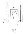
- FIG. 3 is a schematic illustration of device 10 in an exemplified embodiment in which the device comprises two electrically biasable electrode structures 16 and a single cylindrical floating electrode structure 18.
- Figures 4a-b illustrate the electric field and the normalized field intensity gradients ⁇ E ⁇ 2 / ⁇ E ⁇ 2 as obtained from Equations 4 and 5, respectively.
- the results are displayed in the vicinity of the cylindrical floating electrode (the dashed rectangle shown in Figure 3 ).
- the geometric dimensions of the model are normalized by the radius of the cylinder R .
- Figure 4c shows the field intensity gradients in the vicinity of the cylindrical floating electrode structure as a function of the radius of the cylinder R . As shown, the field intensity gradient is inversely proportional to R . Thus, dielectrophoretic forces in the vicinity of a nanoscale floating cylinder are expected to be three orders of magnitude larger than those in the vicinity of a microscale cylinder.
- FIGS 5a-d The model devices are schematically illustrated in Figures 5a-d .
- a first mdel device, illustrated in Figures 5a (top view) and 5b (fragmentary side view) was designed according to a preferred embodiment of the present invention and included both electrically biasable electrode structures and electrically floating electrode structures.
- the electrically biasable electrode structures were arranged in an interdigitated arrangement
- the electrically biasable electrode structures comprise first electrode stem 52 , disposed proximate to the substrate surface 56 and parallel with a second electrode stem 54 , proximate to the same surface.
- the first electrode stem is connected to a first terminal of an AC power source 58
- the second electrode stem is connected to a second terminal of power source 58 , such that that the first electrode stem and the second electrode stem have opposite polarities.
- a series of first electrode “digits" 60 extend in a substantially normal direction from first electrode stem 52 towards second electrode stem 54 , without touching the second electrode stem.
- a series of "digits" 62 of second electrode stem 54 extend in a substantially normal direction from the second electrode stem towards the first electrode stem, without touching the first electrode stem.
- First electrodes digits 60 are spaced so that the digits are adjacent to and substantially parallel with second electrode digits 62 .
- an electrode having one polarity at a given moment is adjacent to one or more electrodes having the opposite polarity.
- the electrically floating electrodes 18 are disposed in the gaps between adjacent electrode digits 60 , 62 . Simulations were performed both for floating electrodes characterized by micrometric dimensions and for floating electrodes characterized by nanometric dimensions.
- the configuration illustrated in Figures 5a-b is referred to hereinunder as the floating electrode dielectrophoresis (feDEP) configuration.
- a second model device illustrated in Figures 5c (top view) and 5d (fragmentary side view) included only electrically biasable electrode structures arranged in an interdigitated arrangement.
- the configuration illustrated in Figures 5c-d is referred to hereinunder as the traditional dielectrophoresis configuration.
- a phase sequence of half a cycle was applied to the biasable electrodes.
- the biasable electrodes were simulated as being applied by alternating voltages of amplitude V 0 .
- the voltages were used as boundary conditions for the simulations.
- the voltages were normalized so as to provide a dimensionless potential ⁇ , defined as the applied voltage divided by V 0 .
- ⁇ alternates between 1 and -1 at the electrodes.
- the model devices for floating electrodes characterized by micrometric dimensions included nine electrodes, enumerated serially from 1 to 9. In the traditional dielectrophoresis configuration, all nine electrodes were biased, and in the floating electrode dielectrophoresis configuration electrode Nos. 3 and 7 were biased and electrodes Nos. 1, 2, 4, 5, 6, 8 and 9 were floating electrodes.
- the model devices for floating electrodes characterized by nanometric dimensions included eight electrodes, enumerated serially from 1 to 8. Electrode Nos. 3 to 6 were floating and electrodes Nos. 1, 2, 7 and 8 were biased electrodes.
- the floating electrodes in the first device were modeled as equipotential perfect electric conductors, and zero tangential electric field was imposed thereat. Additionally, a zero net charge was imposed on each floating electrode.
- a commercial finite element simulation software ANSYS® was used for calculating the electric fields.
- MATLAB® software was used for studying and visualizing the field intensity gradients.
- the electric field generated in the configuration of Figures 5c-d is spatially periodic and can be solved by modeling only a single electrode. Yet, to avoid numeric discrepancies that may occur when a finite element mesh is changed, a single mesh was maintained for all the microscale floating electrode configurations studied. Unlike the configuration in Figure 5c-d , there is a-priori no spatial periodicity when floating electrodes are incorporated. The mesh therefore contained all the nine electrodes used. The geometric dimensions of the models were normalized by the characteristic length of the electrode width, indicated by d in Figures 5b and 5d .
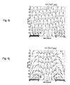
- Figures 6a-j show the dimensionless potential and the electric field intensity (
- Figures c-d show iso-contours of the field intensity for the traditional ( Figure 6c ) and floating electrode ( Figure 6d ) configuration;
- Figures 6e-f show iso-contours of the field intensity gradient for the traditional ( Figure 6e ) and floating electrode ( Figure 6f ) configuration;
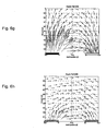
- Figures 6g-h show vector representation of the electric field between two adjacent electrode centers for the traditional ( Figure 6g ) and floating electrode ( Figure 6h ) configuration;
- Figures 6i-j show vector representation of the normalized field intensity gradient between two adjacent electrode centers for the traditional ( Figure 6i ) and floating electrode ( Figure 6j ) configuration.
- Figures 6b , 6d , 6f , 6h and 6j show the simulation results for the floating electrode dielectrophoresis configuration.
- the field intensities and field intensity gradients are substantially different from those of the traditional dielectrophoresis configuration.
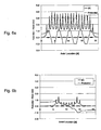
- Figures 7a-b show the results of finite element calculations for the traditional dielectrophoresis device.
- the results relate to a representative region between two adjacent biased microelectrode centers (the dashed rectangle illustrated in Figure 5d ).
- the filled and empty bars at the bottom of each figure represent the biased electrodes (as illustrated in Figure 5d ).
- the highest field intensities and field intensity gradients were obtained at the edges of the biased electrodes.
- Figures 7c-d show the results of finite element calculations for the floating electrode dielectrophoresis configuration in which the floating electrodes were simulated as having micrometric size not in accordance with the present invention.
- the results relate to a representative region between two adjacent floating electrode centers (the dashed rectangle seen in Figure 5b ).
- the patterned bars at the bottom of each figure represent the floating electrodes (as illustrated in Figure 5b ).
- the floating electrode dielectrophoresis configuration resulted in field intensities and field intensity gradients that are different from those of the traditional dielectrophoresis configuration. Nevertheless, the floating electrodes also exhibited the highest field intensities and field intensity gradients at their edges. Therefore, particles are expected to collect at the floating electrode edges as well as at biased electrode edges.
- Figures 8a-h show the results of finite element calculations for the floating electrode dielectrophoresis configuration in which the floating electrode were simulated as having nanometric size. The results are displayed on two different size scales.
- the scale in Figures 8a, 8c , 8e and 8g represents the microscale spacing between the biased electrodes
- the scale in Figures 8b , 8d , 8f and 8h represents the nanoscale spacing between the floating nanoelectrodes.
- the dimensionless potential alternated between 1 and -1 at the biased microelectrodes.
- the floating nanoelectrodes were equipotential, and the potential at each floating nanoelectrode was unique and different from the potential at other floating nanoelectrodes.
- the potential values of the nanoelectrodes were determined by capacitive coupling to the biased microelectrodes, and are consistent with the spatial distribution of the potential imposed by the biased microelectrodes. For the region presented in Figure 8b , located approximately in the middle between adjacent biased microelectrodes, the potential is expected to be nearly zero.
- Figures 8c-d show the obtained electric field values. Maximal values of the electric field were obtained at the electrode edges. There was no significant difference between field intensity values at the biased microelectrodes and field intensity values at the floating nanoelectrodes.
- Figures 8e-h show the electric field intensity and field intensity gradient distributions.
- the electric field intensity and field intensity gradient distributions are shown for a region between adjacent biased microelectrode centers (microscale region).
- the electric field intensity and field intensity gradient distributions are shown for a region between adjacent floating nanoelectrode centers (nanoscale region). In both the microscale and nanoscale regions, the highest field intensities and field intensity gradients were obtained at the electrode edges.
- the electric field values at the biased microelectrodes and at the floating nanoelectrodes are similar ( Figures 8e-f ). Still, the field intensity gradients at the floating nanoelectrodes were increased by a factor of 2500 in comparison to those at the biased microelectrodes ( Figures 8g-h) .
- Figure 9 shows the effect of the distance between the biased electrodes on the field intensity and field intensity gradient at the floating electrode edges, for the floating electrode dielectrophoresis configuration in which the floating electrodes were simulated as having micrometric size.
- the distance between the biased electrodes is a function of the number of floating electrodes located between the biased electrodes.
- the obtained values for the field intensity are shown as filled squares, and the obtained values for field intensity gradient are shown as filled circles. Also shown are curves representing numerical fits to the obtained values.
- the field intensity and field intensity gradient decreased generally exponentially with the distance between the biased electrodes.
- the numerical fit was 2.099 exp(-0.1891x), with a squared Pearson coefficient of 0.9356, and for the field intensity gradient, the numerical fit was 66.831 exp(-0.3949x), with a squared Pearson coefficient of 0.891, where x is the distance between the biased electrodes normalized to the electrode width d as defined in Figures 5b and 5d .
- a prototype device was manufactured in accordance with preferred embodiments of the present invention.
- the prototype device was used for manipulating erythrocytes in blood sample.
- the two electrode configurations were fabricated.
- the two electrode configurations had different feature sizes and were fabricated using different processes and materials.
- each electrode was 12.5 ⁇ m in width, and adjacent electrodes were separated by a 12.5 ⁇ m gap.
- a 200- ⁇ -thick titanium and a 2000- ⁇ -thick gold layers were subsequently deposited on a microscope slide using an electron-beam evaporator.
- the Ti/Au electrodes were obtained using a lift-off process.
- the obtained device included various electrode layouts in an arrangement in which 7-8 floating electrodes were located between or adjacent to two biasable electrodes. The number of the floating electrodes and their arrangement in relation to the biased electrodes was controlled by changing the bias connection from electrode to electrode within the array.
- each electrode was 25 ⁇ m in width and adjacent electrodes were separated by a 25 ⁇ m gap.
- a 7000- ⁇ -thick aluminum layer was deposited on a soda lime glass wafer using an electron-beam evaporator.
- the electrodes were obtained using an aluminum etching process.
- the obtained device included an electrode arrangement in which 7-8 floating electrodes were located between or adjacent to two biasable electrodes. The number of the floating electrodes and their arrangement in relation to the biased electrodes was controlled by changing the bias connection from electrode to electrode within the array.
- Fresh whole blood was obtained from white male Spargue Dawley rats. All animals were older than three months and weighed about 250 grams.
- the blood was drawn from the aorta prior to animal sacrifice into a syringe washed with an anticoagulant (héparine choay, 5000 U.I/1 ml).
- a suspending buffer was prepared by diluting PBS (Dulbecco's Phosphate Buffered Saline - D8662, Sigma Aldrich) with deionized water to give a range of conductivities. Standard dilution of the blood was performed by using the suspending buffer at a 1:100 ratio. The conductivity of the sample was measured using a conductivity meter (Fluke 179).
- the devices were contacted by the sample and a 1 MHz, 10 V (peak to peak) voltage was applied to the biasable electrodes.
- Erythrocyte motion was visually recorded with a Nikon VM Lens adapter on a Nikon SMZ800 microscope equipped with a Sony SSC-M370CE high resolution CCD camera. Digital output from the camera was routed to a computer with a National Instruments IMAQ PCI 1411 video capture card. LabVIEW 7.1 software (National Instruments) was used for controlling the recording parameters. AC voltage was applied to the electrodes from an Agilent HP33220A function generator. Waveforms were monitored with a Tektronix TDS 1002-60 MHz oscilloscope.
- Figures 10a-b show two video images captured in the experiments.
- the biased electrodes are marked by solid lines symbolizing the function generator and the voltage connections.
- the remaining electrodes are floating electrodes.
- the images in the figures correspond to the first prototype device (Ti/Au electrodes, lift-off technique).
- Figures 10a-b demonstrate erythrocyte collection at floating electrode edges, as indicated by white arrows, thus demonstrating that the erythrocytes experienced positive dielectrophoresis.
Landscapes
- Chemical & Material Sciences (AREA)
- Health & Medical Sciences (AREA)
- Life Sciences & Earth Sciences (AREA)
- Engineering & Computer Science (AREA)
- Chemical Kinetics & Catalysis (AREA)
- General Health & Medical Sciences (AREA)
- Organic Chemistry (AREA)
- Physics & Mathematics (AREA)
- Fluid Mechanics (AREA)
- Zoology (AREA)
- Molecular Biology (AREA)
- Wood Science & Technology (AREA)
- Biotechnology (AREA)
- Bioinformatics & Cheminformatics (AREA)
- Biomedical Technology (AREA)
- Genetics & Genomics (AREA)
- Sustainable Development (AREA)
- Cell Biology (AREA)
- Electrochemistry (AREA)
- Biochemistry (AREA)
- General Engineering & Computer Science (AREA)
- Microbiology (AREA)
- Microelectronics & Electronic Packaging (AREA)
- Dispersion Chemistry (AREA)
- Analytical Chemistry (AREA)
- Hematology (AREA)
- Clinical Laboratory Science (AREA)
- Physical Or Chemical Processes And Apparatus (AREA)
- Apparatus Associated With Microorganisms And Enzymes (AREA)
- Electrostatic Separation (AREA)
Claims (14)
- Vorrichtung (80) zum Manipulieren eines in einem Fluid vorhandenen Gegenstands durch Elektrokinetik, wobei die Vorrichtung (80) Folgendes umfasst:ein Substrat (12), das eine Strömungskammer (14) bildet und auf dem mindestens eine elektrisch potentialfreie Elektrodenstruktur (18) mit mindestens einer nanometrischen Abmessung gebildet oder damit integriert ist; undeine elektrisch aktivierbare Vorrichtung (82) mit mehreren elektrisch vorspannbaren Elektrodenstrukturen (16), die dazu gestaltet und ausgeführt ist, das genannte Substrat (12) aufzunehmen und ein elektrisches Feld in einer Region zu erzeugen, mit der das genannte Substrat (12) in Eingriff steht, so dass in Betrieb keine Vorspannung vorliegt, die an die genannte mindestens eine elektrisch potentialfreie Elektrodenstruktur (18) angelegt ist.
- Vorrichtung (80) nach Anspruch 1, wobei mindestens eine der genannten elektrisch vorspannbaren Elektrodenstrukturen (16) durch mindestens eine mikrometrische Abmessung gekennzeichnet ist.
- Vorrichtung (80) nach einem der Ansprüche 1 und 2, wobei die genannte mindestens eine elektrisch potentialfreie Elektrodenstruktur (18) dazu gestaltet und ausgeführt ist, eine auf den Gegenstand ausgeübte dielektrophoretische Kraft um mindestens eine Größenordnung zu erhöhen.
- Vorrichtung (80) nach einem der Ansprüche 1 und 2, wobei die genannte mindestens eine elektrisch potentialfreie Elektrodenstruktur (18) dazu gestaltet und ausgeführt ist, eine auf den Gegenstand ausgeübte dielektrophoretische Kraft um mindestens N Größenordnungen zu erhöhen, wobei das genannte N mindestens 2 ist.
- Vorrichtung (80) nach einem der Ansprüche 1-4, wobei die Vorrichtung weiter mindestens eine zusätzliche elektrisch potentialfreie Elektrodenstruktur (18) umfasst.
- Vorrichtung (80) nach einem der Ansprüche 1-5, wobei die genannten mehreren elektrisch vorspannbaren Elektrodenstrukturen (16) interdigitierte Elektroden umfassen.
- Vorrichtung (80) nach einem der Ansprüche 1-6, wobei die genannten elektrisch potentialfreien Elektrodenstrukturen (18) Kohlenstoffnanoröhren umfassen.
- Vorrichtung (80) nach einem der Ansprüche 1-7, weiter umfassend eine Leistungsquellenvorrichtung (32), die elektrisch mit den genannten mehreren elektrisch vorspannbaren Elektrodenstrukturen (16) verbunden ist und dazu ausgebildet ist, Vorspannung an diese anzulegen.
- Vorrichtung (80) nach Anspruch 8, wobei die genannte Leistungsquellenvorrichtung (32) dazu ausgebildet ist, phasenverschobene Signale an Einzelne der genannten mehreren Elektroden bereitzustellen.
- Vorrichtung (80) nach Anspruch 9, wobei die genannten phasenverschobenen Signale derart ausgewählt sind, dass sie eine dielektrophoretische Wanderwellenkraft erzeugen.
- Vorrichtung (80) nach Anspruch 9, wobei die genannten phasenverschobenen Signale derart ausgewählt sind, dass sie eine klassische dielektrophoretische Kraft erzeugen.
- Verfahren zum Manipulieren eines in einem Fluid vorhandenen Gegenstands durch Elektrokinetik, umfassend das Berühren des Fluids mit der Vorrichtung (80) nach einem der Ansprüche 1-11 und das Anlegen von Vorspannung an die genannten mehreren elektrisch vorspannbaren Elektrodenstrukturen (16), um ein uneinheitliches elektrisches Feld zu erzeugen, wodurch der Gegenstand manipuliert wird.
- Verfahren nach Anspruch 12, wobei das genannte Fluid aus der Gruppe ausgewählt wird, die besteht aus: Wasser, einer Bakterienzellensuspension, einem Proteinmedium, einem Antikörpermedium, einem Nukleinsäuremedium, Tinte, phosphatgepufferter Salzlösung und einem biologischen Fluid.
- Verfahren nach Anspruch 12, wobei der genannte Gegenstand ausgewählt ist aus der Gruppe, die besteht aus: einer Zelle, einer Zellenanhäufung, einem normalen Erythrozyt, einem abnormalen Erythrozyt, einer fötalen kernhaltigen roten Blutzelle, einer Krebszelle, einem Protein, DNA, RNA, einem Antikörper, einem Antigen, einem Lipid, einer Ansammlung von Molekülen, einem Virus, einem Plasmid, einem Bakterium, einem Protozoon, einem Mineral, einem Kristall, einem leitfähigen Partikel, einem halbleitenden Partikel, einem dielektrischen Partikel und einer Gasblase.
Applications Claiming Priority (2)
| Application Number | Priority Date | Filing Date | Title |
|---|---|---|---|
| US79054706P | 2006-04-10 | 2006-04-10 | |
| PCT/IL2007/000460 WO2007116406A1 (en) | 2006-04-10 | 2007-04-10 | Method and device for electrokinetic manipulation |
Publications (2)
| Publication Number | Publication Date |
|---|---|
| EP2010323A1 EP2010323A1 (de) | 2009-01-07 |
| EP2010323B1 true EP2010323B1 (de) | 2012-11-14 |
Family
ID=38234461
Family Applications (1)
| Application Number | Title | Priority Date | Filing Date |
|---|---|---|---|
| EP07736200A Not-in-force EP2010323B1 (de) | 2006-04-10 | 2007-04-10 | Verfahren und vorrichtung zur elektrokinetischen handhabung |
Country Status (3)
| Country | Link |
|---|---|
| US (1) | US20090314644A1 (de) |
| EP (1) | EP2010323B1 (de) |
| WO (1) | WO2007116406A1 (de) |
Families Citing this family (21)
| Publication number | Priority date | Publication date | Assignee | Title |
|---|---|---|---|---|
| WO2009004533A1 (en) * | 2007-07-03 | 2009-01-08 | Nxp B.V. | A microfluidic chip for and a method of handling fluidic droplets |
| US8308926B2 (en) | 2007-08-20 | 2012-11-13 | Purdue Research Foundation | Microfluidic pumping based on dielectrophoresis |
| US8716655B2 (en) * | 2009-07-02 | 2014-05-06 | Tricorntech Corporation | Integrated ion separation spectrometer |
| FR2963445B1 (fr) * | 2010-08-02 | 2013-05-03 | Nanomade Concept | Surface tactile et procede de fabrication d'une telle surface |
| US9196457B2 (en) * | 2011-05-24 | 2015-11-24 | The Trustees Of The University Of Pennsylvania | Flow cells for electron microscope imaging with multiple flow streams |
| JP6114270B2 (ja) * | 2011-08-02 | 2017-04-12 | 東京エレクトロン株式会社 | 電界によりパターン及び構造形成を制御する方法及びデバイス |
| JP2015519886A (ja) | 2012-04-16 | 2015-07-16 | バイオロジカル ダイナミクス,インク. | 核酸サンプル調製 |
| US8932815B2 (en) | 2012-04-16 | 2015-01-13 | Biological Dynamics, Inc. | Nucleic acid sample preparation |
| EP3129481A4 (de) | 2014-04-08 | 2017-10-25 | Biological Dynamics, Inc. | Verbesserte vorrichtungen zur trennung von biologischen materialien |
| US9310328B1 (en) | 2015-06-17 | 2016-04-12 | King Abdulaziz University | Method of detecting leukemia |
| WO2017165852A1 (en) | 2016-03-24 | 2017-09-28 | Biological Dynamics, Inc. | Disposable fluidic cartridge and components |
| US10558204B2 (en) * | 2016-09-19 | 2020-02-11 | Palo Alto Research Center Incorporated | System and method for scalable real-time micro-object position control with the aid of a digital computer |
| US10413913B2 (en) | 2017-02-15 | 2019-09-17 | Tokyo Electron Limited | Methods and systems for dielectrophoresis (DEP) separation |
| WO2018208820A1 (en) | 2017-05-08 | 2018-11-15 | Biological Dynamics, Inc. | Methods and systems for analyte information processing |
| WO2019126388A1 (en) | 2017-12-19 | 2019-06-27 | Biological Dynamics, Inc. | Methods and devices for detection of multiple analytes from a biological sample |
| WO2019195196A1 (en) | 2018-04-02 | 2019-10-10 | Biological Dynamics, Inc. | Dielectric materials |
| US12204085B2 (en) * | 2018-04-27 | 2025-01-21 | Hewlett-Packard Development Company, L.P. | Nonrotating nonuniform electric field object rotation |
| JP7348454B2 (ja) | 2018-10-01 | 2023-09-21 | 東京エレクトロン株式会社 | 基板表面から異物を静電的に除去するための装置及び方法 |
| JP7278755B2 (ja) * | 2018-11-26 | 2023-05-22 | Nissha株式会社 | フォトマスクおよび捕集ユニットのベース |
| US20200333286A1 (en) * | 2019-04-18 | 2020-10-22 | University Of Florida Research Foundation, Inc. | Modularized inexpensive detection of cerebral spinal fluid for medical applications |
| CN115475669A (zh) * | 2022-09-15 | 2022-12-16 | 上海科技大学 | 一种液滴微流控芯片 |
Citations (1)
| Publication number | Priority date | Publication date | Assignee | Title |
|---|---|---|---|---|
| WO2006004558A1 (en) * | 2004-07-06 | 2006-01-12 | Agency For Science, Technology And Research | Biochip for sorting and lysing biological samples |
Family Cites Families (7)
| Publication number | Priority date | Publication date | Assignee | Title |
|---|---|---|---|---|
| US6203683B1 (en) * | 1998-11-09 | 2001-03-20 | Princeton University | Electrodynamically focused thermal cycling device |
| US20050221423A1 (en) * | 2002-04-10 | 2005-10-06 | Andersen Jens T | Bacillus host cell |
| US20040011650A1 (en) * | 2002-07-22 | 2004-01-22 | Frederic Zenhausern | Method and apparatus for manipulating polarizable analytes via dielectrophoresis |
| EP1548103A4 (de) * | 2002-08-20 | 2008-06-25 | Sony Corp | Hybridisierung-wahrnehmendes teil, sensor-chip und hybridisierungsverfahren |
| US6911132B2 (en) * | 2002-09-24 | 2005-06-28 | Duke University | Apparatus for manipulating droplets by electrowetting-based techniques |
| US20050221473A1 (en) * | 2004-03-30 | 2005-10-06 | Intel Corporation | Sensor array integrated circuits |
| EP1764418B1 (de) * | 2005-09-14 | 2012-08-22 | STMicroelectronics Srl | Verfahren und Vorrichtung zur Behandlung biologischer Proben mittels Dielektrophorese |
-
2007
- 2007-04-10 EP EP07736200A patent/EP2010323B1/de not_active Not-in-force
- 2007-04-10 WO PCT/IL2007/000460 patent/WO2007116406A1/en not_active Ceased
- 2007-04-10 US US12/225,880 patent/US20090314644A1/en not_active Abandoned
Patent Citations (1)
| Publication number | Priority date | Publication date | Assignee | Title |
|---|---|---|---|---|
| WO2006004558A1 (en) * | 2004-07-06 | 2006-01-12 | Agency For Science, Technology And Research | Biochip for sorting and lysing biological samples |
Also Published As
| Publication number | Publication date |
|---|---|
| US20090314644A1 (en) | 2009-12-24 |
| EP2010323A1 (de) | 2009-01-07 |
| WO2007116406A1 (en) | 2007-10-18 |
Similar Documents
| Publication | Publication Date | Title |
|---|---|---|
| EP2010323B1 (de) | Verfahren und vorrichtung zur elektrokinetischen handhabung | |
| Gagnon et al. | Aligning fast alternating current electroosmotic flow fields and characteristic frequencies with dielectrophoretic traps to achieve rapid bacteria detection | |
| Pethig | Where is dielectrophoresis (DEP) going? | |
| US9995668B2 (en) | Apparatus for manipulating, modifying and characterizing particles in a micro channel | |
| Hughes | Strategies for dielectrophoretic separation in laboratory‐on‐a‐chip systems | |
| US6596143B1 (en) | Apparatus for switching and manipulating particles and method of use thereof | |
| CN102866193B (zh) | 基于介电泳来操控液体中的粒子的器件及方法 | |
| Kadaksham et al. | Dielectrophoresis induced clustering regimes of viable yeast cells | |
| US7419574B2 (en) | Dielectrophoresis device and method having non-uniform arrays for manipulating particles | |
| US20020036139A1 (en) | Method and apparatus for programmable fluidic processing | |
| WO2007070592A2 (en) | Three dimensional dielectrophorectic separator and methods of use | |
| CN110352096A (zh) | 多平面微电极阵列装置及其制造和使用方法 | |
| Yu et al. | Sequential field-flow cell separation method in a dielectrophoretic chip with 3-D electrodes | |
| JP2009014342A (ja) | 誘電泳動チップおよび誘電泳動装置並びに誘電泳動システム | |
| US20080296157A1 (en) | Method and Device for Handling Sedimenting Particles | |
| Sano et al. | Simultaneous electrokinetic flow and dielectrophoretic trapping using perpendicular static and dynamic electric fields | |
| US20090294291A1 (en) | Iso-dielectric separation apparatus and methods of use | |
| EP1919627A1 (de) | Mikroelektrodenvorrichtung zur dielektrophoretischen charakterisierung von partikeln | |
| KR102443561B1 (ko) | 독립형 부유 전극 구조의 입자 포집 장치 및 이를 이용한 입자 포집 방법 | |
| Lejard-Malki et al. | Selective electrohydrodynamic concentration of waterborne parasites on a chip | |
| Abdelhamid et al. | Dielectrophoretic based Microfluidic for nanoparticles “viruses” separation | |
| US8246802B2 (en) | Small volume liquid manipulation, method, apparatus and process | |
| EP3842146B1 (de) | Verfahren und vorrichtung zur kontinuierlichen trennung von komponenten aus einer probe | |
| Lin | Cell manipulations with dielectrophoresis | |
| EP4670843A1 (de) | Modul zur trennung eines analyten von einem schadstoff |
Legal Events
| Date | Code | Title | Description |
|---|---|---|---|
| PUAI | Public reference made under article 153(3) epc to a published international application that has entered the european phase |
Free format text: ORIGINAL CODE: 0009012 |
|
| 17P | Request for examination filed |
Effective date: 20081021 |
|
| AK | Designated contracting states |
Kind code of ref document: A1 Designated state(s): AT BE BG CH CY CZ DE DK EE ES FI FR GB GR HU IE IS IT LI LT LU LV MC MT NL PL PT RO SE SI SK TR |
|
| AX | Request for extension of the european patent |
Extension state: AL BA HR MK RS |
|
| 17Q | First examination report despatched |
Effective date: 20090302 |
|
| GRAP | Despatch of communication of intention to grant a patent |
Free format text: ORIGINAL CODE: EPIDOSNIGR1 |
|
| DAX | Request for extension of the european patent (deleted) | ||
| GRAS | Grant fee paid |
Free format text: ORIGINAL CODE: EPIDOSNIGR3 |
|
| GRAA | (expected) grant |
Free format text: ORIGINAL CODE: 0009210 |
|
| AK | Designated contracting states |
Kind code of ref document: B1 Designated state(s): AT BE BG CH CY CZ DE DK EE ES FI FR GB GR HU IE IS IT LI LT LU LV MC MT NL PL PT RO SE SI SK TR |
|
| REG | Reference to a national code |
Ref country code: GB Ref legal event code: FG4D |
|
| REG | Reference to a national code |
Ref country code: CH Ref legal event code: EP Ref country code: AT Ref legal event code: REF Ref document number: 583655 Country of ref document: AT Kind code of ref document: T Effective date: 20121115 |
|
| REG | Reference to a national code |
Ref country code: IE Ref legal event code: FG4D |
|
| REG | Reference to a national code |
Ref country code: DE Ref legal event code: R096 Ref document number: 602007026683 Country of ref document: DE Effective date: 20130103 |
|
| REG | Reference to a national code |
Ref country code: NL Ref legal event code: VDEP Effective date: 20121114 |
|
| REG | Reference to a national code |
Ref country code: AT Ref legal event code: MK05 Ref document number: 583655 Country of ref document: AT Kind code of ref document: T Effective date: 20121114 |
|
| REG | Reference to a national code |
Ref country code: LT Ref legal event code: MG4D |
|
| PG25 | Lapsed in a contracting state [announced via postgrant information from national office to epo] |
Ref country code: ES Free format text: LAPSE BECAUSE OF FAILURE TO SUBMIT A TRANSLATION OF THE DESCRIPTION OR TO PAY THE FEE WITHIN THE PRESCRIBED TIME-LIMIT Effective date: 20130225 Ref country code: FI Free format text: LAPSE BECAUSE OF FAILURE TO SUBMIT A TRANSLATION OF THE DESCRIPTION OR TO PAY THE FEE WITHIN THE PRESCRIBED TIME-LIMIT Effective date: 20121114 Ref country code: SE Free format text: LAPSE BECAUSE OF FAILURE TO SUBMIT A TRANSLATION OF THE DESCRIPTION OR TO PAY THE FEE WITHIN THE PRESCRIBED TIME-LIMIT Effective date: 20121114 Ref country code: LT Free format text: LAPSE BECAUSE OF FAILURE TO SUBMIT A TRANSLATION OF THE DESCRIPTION OR TO PAY THE FEE WITHIN THE PRESCRIBED TIME-LIMIT Effective date: 20121114 |
|
| PG25 | Lapsed in a contracting state [announced via postgrant information from national office to epo] |
Ref country code: PL Free format text: LAPSE BECAUSE OF FAILURE TO SUBMIT A TRANSLATION OF THE DESCRIPTION OR TO PAY THE FEE WITHIN THE PRESCRIBED TIME-LIMIT Effective date: 20121114 Ref country code: GR Free format text: LAPSE BECAUSE OF FAILURE TO SUBMIT A TRANSLATION OF THE DESCRIPTION OR TO PAY THE FEE WITHIN THE PRESCRIBED TIME-LIMIT Effective date: 20130215 Ref country code: SI Free format text: LAPSE BECAUSE OF FAILURE TO SUBMIT A TRANSLATION OF THE DESCRIPTION OR TO PAY THE FEE WITHIN THE PRESCRIBED TIME-LIMIT Effective date: 20121114 Ref country code: PT Free format text: LAPSE BECAUSE OF FAILURE TO SUBMIT A TRANSLATION OF THE DESCRIPTION OR TO PAY THE FEE WITHIN THE PRESCRIBED TIME-LIMIT Effective date: 20130314 Ref country code: BE Free format text: LAPSE BECAUSE OF FAILURE TO SUBMIT A TRANSLATION OF THE DESCRIPTION OR TO PAY THE FEE WITHIN THE PRESCRIBED TIME-LIMIT Effective date: 20121114 Ref country code: LV Free format text: LAPSE BECAUSE OF FAILURE TO SUBMIT A TRANSLATION OF THE DESCRIPTION OR TO PAY THE FEE WITHIN THE PRESCRIBED TIME-LIMIT Effective date: 20121114 Ref country code: CY Free format text: LAPSE BECAUSE OF FAILURE TO SUBMIT A TRANSLATION OF THE DESCRIPTION OR TO PAY THE FEE WITHIN THE PRESCRIBED TIME-LIMIT Effective date: 20121114 |
|
| PG25 | Lapsed in a contracting state [announced via postgrant information from national office to epo] |
Ref country code: AT Free format text: LAPSE BECAUSE OF FAILURE TO SUBMIT A TRANSLATION OF THE DESCRIPTION OR TO PAY THE FEE WITHIN THE PRESCRIBED TIME-LIMIT Effective date: 20121114 |
|
| PG25 | Lapsed in a contracting state [announced via postgrant information from national office to epo] |
Ref country code: DK Free format text: LAPSE BECAUSE OF FAILURE TO SUBMIT A TRANSLATION OF THE DESCRIPTION OR TO PAY THE FEE WITHIN THE PRESCRIBED TIME-LIMIT Effective date: 20121114 Ref country code: SK Free format text: LAPSE BECAUSE OF FAILURE TO SUBMIT A TRANSLATION OF THE DESCRIPTION OR TO PAY THE FEE WITHIN THE PRESCRIBED TIME-LIMIT Effective date: 20121114 Ref country code: EE Free format text: LAPSE BECAUSE OF FAILURE TO SUBMIT A TRANSLATION OF THE DESCRIPTION OR TO PAY THE FEE WITHIN THE PRESCRIBED TIME-LIMIT Effective date: 20121114 Ref country code: BG Free format text: LAPSE BECAUSE OF FAILURE TO SUBMIT A TRANSLATION OF THE DESCRIPTION OR TO PAY THE FEE WITHIN THE PRESCRIBED TIME-LIMIT Effective date: 20130214 Ref country code: CZ Free format text: LAPSE BECAUSE OF FAILURE TO SUBMIT A TRANSLATION OF THE DESCRIPTION OR TO PAY THE FEE WITHIN THE PRESCRIBED TIME-LIMIT Effective date: 20121114 |
|
| PG25 | Lapsed in a contracting state [announced via postgrant information from national office to epo] |
Ref country code: IT Free format text: LAPSE BECAUSE OF FAILURE TO SUBMIT A TRANSLATION OF THE DESCRIPTION OR TO PAY THE FEE WITHIN THE PRESCRIBED TIME-LIMIT Effective date: 20121114 Ref country code: NL Free format text: LAPSE BECAUSE OF FAILURE TO SUBMIT A TRANSLATION OF THE DESCRIPTION OR TO PAY THE FEE WITHIN THE PRESCRIBED TIME-LIMIT Effective date: 20121114 Ref country code: RO Free format text: LAPSE BECAUSE OF FAILURE TO SUBMIT A TRANSLATION OF THE DESCRIPTION OR TO PAY THE FEE WITHIN THE PRESCRIBED TIME-LIMIT Effective date: 20121114 |
|
| PLBE | No opposition filed within time limit |
Free format text: ORIGINAL CODE: 0009261 |
|
| STAA | Information on the status of an ep patent application or granted ep patent |
Free format text: STATUS: NO OPPOSITION FILED WITHIN TIME LIMIT |
|
| 26N | No opposition filed |
Effective date: 20130815 |
|
| PG25 | Lapsed in a contracting state [announced via postgrant information from national office to epo] |
Ref country code: MC Free format text: LAPSE BECAUSE OF FAILURE TO SUBMIT A TRANSLATION OF THE DESCRIPTION OR TO PAY THE FEE WITHIN THE PRESCRIBED TIME-LIMIT Effective date: 20121114 |
|
| REG | Reference to a national code |
Ref country code: CH Ref legal event code: PL |
|
| REG | Reference to a national code |
Ref country code: DE Ref legal event code: R097 Ref document number: 602007026683 Country of ref document: DE Effective date: 20130815 |
|
| REG | Reference to a national code |
Ref country code: IE Ref legal event code: MM4A |
|
| PG25 | Lapsed in a contracting state [announced via postgrant information from national office to epo] |
Ref country code: CH Free format text: LAPSE BECAUSE OF NON-PAYMENT OF DUE FEES Effective date: 20130430 Ref country code: LI Free format text: LAPSE BECAUSE OF NON-PAYMENT OF DUE FEES Effective date: 20130430 |
|
| PG25 | Lapsed in a contracting state [announced via postgrant information from national office to epo] |
Ref country code: IE Free format text: LAPSE BECAUSE OF NON-PAYMENT OF DUE FEES Effective date: 20130410 |
|
| PG25 | Lapsed in a contracting state [announced via postgrant information from national office to epo] |
Ref country code: MT Free format text: LAPSE BECAUSE OF FAILURE TO SUBMIT A TRANSLATION OF THE DESCRIPTION OR TO PAY THE FEE WITHIN THE PRESCRIBED TIME-LIMIT Effective date: 20121114 |
|
| REG | Reference to a national code |
Ref country code: FR Ref legal event code: PLFP Year of fee payment: 9 |
|
| PG25 | Lapsed in a contracting state [announced via postgrant information from national office to epo] |
Ref country code: TR Free format text: LAPSE BECAUSE OF FAILURE TO SUBMIT A TRANSLATION OF THE DESCRIPTION OR TO PAY THE FEE WITHIN THE PRESCRIBED TIME-LIMIT Effective date: 20121114 |
|
| PG25 | Lapsed in a contracting state [announced via postgrant information from national office to epo] |
Ref country code: HU Free format text: LAPSE BECAUSE OF FAILURE TO SUBMIT A TRANSLATION OF THE DESCRIPTION OR TO PAY THE FEE WITHIN THE PRESCRIBED TIME-LIMIT; INVALID AB INITIO Effective date: 20070410 Ref country code: LU Free format text: LAPSE BECAUSE OF NON-PAYMENT OF DUE FEES Effective date: 20130410 |
|
| PGFP | Annual fee paid to national office [announced via postgrant information from national office to epo] |
Ref country code: DE Payment date: 20150421 Year of fee payment: 9 Ref country code: GB Payment date: 20150420 Year of fee payment: 9 |
|
| PGFP | Annual fee paid to national office [announced via postgrant information from national office to epo] |
Ref country code: FR Payment date: 20150421 Year of fee payment: 9 |
|
| PG25 | Lapsed in a contracting state [announced via postgrant information from national office to epo] |
Ref country code: IS Free format text: LAPSE BECAUSE OF FAILURE TO SUBMIT A TRANSLATION OF THE DESCRIPTION OR TO PAY THE FEE WITHIN THE PRESCRIBED TIME-LIMIT Effective date: 20121114 |
|
| REG | Reference to a national code |
Ref country code: DE Ref legal event code: R119 Ref document number: 602007026683 Country of ref document: DE |
|
| GBPC | Gb: european patent ceased through non-payment of renewal fee |
Effective date: 20160410 |
|
| REG | Reference to a national code |
Ref country code: FR Ref legal event code: ST Effective date: 20161230 |
|
| PG25 | Lapsed in a contracting state [announced via postgrant information from national office to epo] |
Ref country code: DE Free format text: LAPSE BECAUSE OF NON-PAYMENT OF DUE FEES Effective date: 20161101 Ref country code: FR Free format text: LAPSE BECAUSE OF NON-PAYMENT OF DUE FEES Effective date: 20160502 Ref country code: GB Free format text: LAPSE BECAUSE OF NON-PAYMENT OF DUE FEES Effective date: 20160410 |