EP2012094A1 - Procede et dispositif de detection de position - Google Patents
Procede et dispositif de detection de position Download PDFInfo
- Publication number
- EP2012094A1 EP2012094A1 EP07742549A EP07742549A EP2012094A1 EP 2012094 A1 EP2012094 A1 EP 2012094A1 EP 07742549 A EP07742549 A EP 07742549A EP 07742549 A EP07742549 A EP 07742549A EP 2012094 A1 EP2012094 A1 EP 2012094A1
- Authority
- EP
- European Patent Office
- Prior art keywords
- magnetic
- magnetic detecting
- detecting element
- output
- output voltage
- Prior art date
- Legal status (The legal status is an assumption and is not a legal conclusion. Google has not performed a legal analysis and makes no representation as to the accuracy of the status listed.)
- Ceased
Links
Images




Classifications
-
- G—PHYSICS
- G01—MEASURING; TESTING
- G01D—MEASURING NOT SPECIALLY ADAPTED FOR A SPECIFIC VARIABLE; ARRANGEMENTS FOR MEASURING TWO OR MORE VARIABLES NOT COVERED IN A SINGLE OTHER SUBCLASS; TARIFF METERING APPARATUS; MEASURING OR TESTING NOT OTHERWISE PROVIDED FOR
- G01D5/00—Mechanical means for transferring the output of a sensing member; Means for converting the output of a sensing member to another variable where the form or nature of the sensing member does not constrain the means for converting; Transducers not specially adapted for a specific variable
- G01D5/12—Mechanical means for transferring the output of a sensing member; Means for converting the output of a sensing member to another variable where the form or nature of the sensing member does not constrain the means for converting; Transducers not specially adapted for a specific variable using electric or magnetic means
- G01D5/14—Mechanical means for transferring the output of a sensing member; Means for converting the output of a sensing member to another variable where the form or nature of the sensing member does not constrain the means for converting; Transducers not specially adapted for a specific variable using electric or magnetic means influencing the magnitude of a current or voltage
- G01D5/142—Mechanical means for transferring the output of a sensing member; Means for converting the output of a sensing member to another variable where the form or nature of the sensing member does not constrain the means for converting; Transducers not specially adapted for a specific variable using electric or magnetic means influencing the magnitude of a current or voltage using Hall-effect devices
- G01D5/145—Mechanical means for transferring the output of a sensing member; Means for converting the output of a sensing member to another variable where the form or nature of the sensing member does not constrain the means for converting; Transducers not specially adapted for a specific variable using electric or magnetic means influencing the magnitude of a current or voltage using Hall-effect devices influenced by the relative movement between the Hall device and magnetic fields
-
- G—PHYSICS
- G01—MEASURING; TESTING
- G01B—MEASURING LENGTH, THICKNESS OR SIMILAR LINEAR DIMENSIONS; MEASURING ANGLES; MEASURING AREAS; MEASURING IRREGULARITIES OF SURFACES OR CONTOURS
- G01B7/00—Measuring arrangements characterised by the use of electric or magnetic techniques
-
- G—PHYSICS
- G01—MEASURING; TESTING
- G01B—MEASURING LENGTH, THICKNESS OR SIMILAR LINEAR DIMENSIONS; MEASURING ANGLES; MEASURING AREAS; MEASURING IRREGULARITIES OF SURFACES OR CONTOURS
- G01B7/00—Measuring arrangements characterised by the use of electric or magnetic techniques
- G01B7/004—Measuring arrangements characterised by the use of electric or magnetic techniques for measuring coordinates of points
-
- G—PHYSICS
- G01—MEASURING; TESTING
- G01D—MEASURING NOT SPECIALLY ADAPTED FOR A SPECIFIC VARIABLE; ARRANGEMENTS FOR MEASURING TWO OR MORE VARIABLES NOT COVERED IN A SINGLE OTHER SUBCLASS; TARIFF METERING APPARATUS; MEASURING OR TESTING NOT OTHERWISE PROVIDED FOR
- G01D5/00—Mechanical means for transferring the output of a sensing member; Means for converting the output of a sensing member to another variable where the form or nature of the sensing member does not constrain the means for converting; Transducers not specially adapted for a specific variable
- G01D5/12—Mechanical means for transferring the output of a sensing member; Means for converting the output of a sensing member to another variable where the form or nature of the sensing member does not constrain the means for converting; Transducers not specially adapted for a specific variable using electric or magnetic means
- G01D5/14—Mechanical means for transferring the output of a sensing member; Means for converting the output of a sensing member to another variable where the form or nature of the sensing member does not constrain the means for converting; Transducers not specially adapted for a specific variable using electric or magnetic means influencing the magnitude of a current or voltage
-
- G—PHYSICS
- G03—PHOTOGRAPHY; CINEMATOGRAPHY; ANALOGOUS TECHNIQUES USING WAVES OTHER THAN OPTICAL WAVES; ELECTROGRAPHY; HOLOGRAPHY
- G03B—APPARATUS OR ARRANGEMENTS FOR TAKING PHOTOGRAPHS OR FOR PROJECTING OR VIEWING THEM; APPARATUS OR ARRANGEMENTS EMPLOYING ANALOGOUS TECHNIQUES USING WAVES OTHER THAN OPTICAL WAVES; ACCESSORIES THEREFOR
- G03B13/00—Viewfinders; Focusing aids for cameras; Means for focusing for cameras; Autofocus systems for cameras
- G03B13/32—Means for focusing
- G03B13/34—Power focusing
- G03B13/36—Autofocus systems
Definitions
- the present invention relates to a position detecting device and a position detecting method, and more particularly to a position detecting device and a position detecting method for detecting the origin of an autofocus or zoom position of a camera.
- a position detecting sensor a sensor using a photo interrupter (transmission photo sensor) or a photo reflector (reflection photo sensor) is known.
- the photo interrupter is a sensor that has a structure where a light-emitting element for converting an electric signal to an optical signal and a light-receiving element for converting an optical signal to an electric signal are faced to each other with fixed spacing and are integrated into a single housing, and that detects the presence or absence of an object according to changes in quantity of light caused by light passing through the two elements.
- the photo reflector is a sensor that has a structure where a light-emitting element for converting an electric signal to an optical signal and a light-receiving element for converting an optical signal to an electric signal are placed on the same side and are integrated into a single housing, and that detects changes in reflected light from an object.
- a device described in Patent Document 1 uses a photo interrupter as a position detecting sensor, and has a sensor for detecting the original position of a zoom lens unit or focus lens unit driven in the direction of the optical axis, the sensor being mounted on a lens barrel having a zoom function or focusing function of the digital still camera.
- the detection of the original position is carried out by using a screening component and a photo interrupter mounted on the lens unit, by driving the lens unit with a motor, by screening light with the screening component when it is moved together with the lens unit and crosses a photosensor, and by monitoring the output level of the photosensor.
- a device described in Patent Document 2 employs a photo reflector as a position detecting sensor, has the photo reflector fixed to one of the two relatively rotating components, a fixed collar, for example, and has a reflective component (reflective sheet) fixed with an adhesive to the other component, a rotating collar, for example. Both the photo reflector and reflective component are fixed to predetermined positions so that the origin detection is made at the position where the output of the photo reflector is produced.
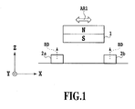
- FIG. 1 and FIG. 2 are block diagrams for explaining a conventional position detecting device based on a magnetic sensor:
- FIG. 1 is a diagram showing a position detecting sensor comprising a magnet and Hall elements;
- FIG. 2 is a diagram showing a signal processing circuit of the position detecting device incorporating the position detecting sensor shown in FIG. 1 .
- the position detecting sensor has one magnet (magnetic flux generating body) 1 and two Hall elements (such as a pair of Hall elements (a magnetic sensor pair)) 2a and 2b placed separately from each other.
- the magnet 1 has a cylindrical shape, whose top side and bottom side are magnetized to the N-pole and the S-pole, respectively.
- the pair of the Hall elements 2a and 2b are fixed to a fixing side body (fixing component) such as a device body, and the magnet 1 is fixed to a moving side body (moving component) that moves with respect to the fixing component. Then, the magnet 1 fixed to the moving component can move in the direction of the arrow AR1 (X direction) with respect to the Hall element pair 2a and 2b fixed to the fixing component.
- symbols BD each designate a magnetic flux detection axis.
- the signal processing circuit 3 shown in FIG. 2 has differential amplifying sections 11a and 11b, a subtracting section 13 and a low-pass filter 15.
- the differential amplifying section 11a obtains Halle. m. f. Vha, the difference between output potentials Va1 and Va2 of the Hall element 2a; and the differential amplifying section 11b obtains Hall e.m.f. Vhb, the difference between output potentials Vb1 and Vb2 of the Hall element 2b.
- the output value from the subtracting section 13 passes through the low-pass filter 15, and is output as an output (position output) indicating the position of the magnet 1.
- the signal processing circuit 3 further comprises an adding section 14, an arithmetic section 16, and a power control section 17; and these processing sections 14, 16 and 17 control the input voltage Vin to each of the Hall elements 2a and 2b in such a manner that the addition value (sum) of the output voltages (Hall e.m.f.) Vha and Vhb becomes constant.
- the signal processing circuit 3 is configured in order that while it controls the input value Vin to the Hall element pair 2a and 2b in such a manner that the addition value (Vha + Vhb) of the output values of the Hall element pair 2a and 2b becomes a constant value Vct, it detects the difference value ⁇ V between the output values of the Hall element pair 2a and 2b, and outputs as the position output.
- the foregoing position detecting device incorporating the position detecting sensor including the magnet and the Hall elements has looseness in the moving mechanism (looseness in the vertical direction of the magnet) in general, which presents a problem of causing an error.
- the photo interrupter detects the position in the horizontal direction without detecting the looseness in the vertical direction.
- the present invention is implemented to solve the foregoing problems. Therefore it is an object of the present invention to provide a position detecting device and a position detecting method that enable cancellation of variation in the temperature characteristics and elimination of an error due to the looseness in the vertical direction by calculating a ratio between the output voltages of a plurality of Hall elements, and that enable miniaturization.
- Patent Document 1 Japanese Patent Laid-Open No. 2006-58818
- Patent Document 2 Japanese Patent Laid-Open No. 2004-132751
- Patent Document 3 Japanese Patent Laid-Open No. 2005-331399 .
- the present invention is implemented to achieve the object, and the invention described in Claim 1 is characterized by comprising: a plurality of magnetic detecting elements placed separately from each other; a magnetic flux generating body that moves relatively to the magnetic detecting elements; and deciding means for making a decision of an original position by using changes in a ratio between output voltages of the magnetic detecting elements.
- the deciding means can comprise a control section for feedback controlling the output voltage from a first magnetic detecting element of the magnetic detecting elements at a constant value; and a driving section for driving a second magnetic detecting element of the magnetic detecting elements by a same driving current as a driving current supplied to the first magnetic detecting element when the control section controls the output voltage at the constant value, and the deciding means obtains as its output a ratio between the output voltage of the first magnetic detecting element and the output voltage of the second magnetic detecting element.
- the position detecting device can operate in a condition that an absolute value of magnetic flux density the first magnetic detecting element and the second magnetic detecting element each detect is a certain value excluding zero.
- control section can comprise a function of adding a reference voltage to the output voltage of the first magnetic detecting element; and a function of adjusting the output voltage of the first magnetic detecting element at the constant value.
- the position detecting device can comprise a feedback sample and hold circuit placed at a stage previous to the control section, for sampling the output signal of the first magnetic detecting element; and a sample and hold circuit placed at an output stage, for sampling the output signal of the second magnetic detecting element.
- the position detecting device can make a decision of a loaded or unloaded state of the magnetic flux generating body according to an output of the ratio between the output voltages of the magnetic detecting elements.
- the magnetic detecting elements can be Hall elements.
- the position detecting method can operate in a condition that an absolute value of the magnetic flux density the first magnetic detecting element and the second magnetic detecting element each detect is a certain value excluding zero.
- the magnetic detecting elements can be Hall elements.
- the present invention since it comprises a plurality of magnetic detecting elements placed separately from each other; a magnetic flux generating body that moves relatively to the magnetic detecting elements; and deciding means for making a decision of an original position by using changes in a ratio between output voltages of the magnetic detecting elements, it can realize the position detecting device and position detecting method capable of eliminating variation in temperature characteristics and canceling an error due to looseness in a vertical direction by calculating the ratio between output voltages of the plurality of Hall elements, and capable of miniaturization.
- the present invention since the present invention employs a division method (ratio) whose output becomes one (ratio) at the origin, but becomes zero when the magnet is removed, it can make a loaded or unloaded decision of the magnet.
- FIG. 3A and FIG. 3B are diagrams for comparing the position detecting sensor based on the division method in accordance with the present invention with the position detecting sensor based on the conventional subtraction method.
- FIG. 3A is a diagram for explaining the subtraction method
- FIG. 3B is a diagram for explaining the division method.
- the reference numeral 21 designates a magnet
- 22a and 22b designate Hall elements HE1 and HE2, respectively.
- Each position detecting sensor has one magnet 21 and two Hall elements 22a and 22b which are placed separately from each other.
- the Hall elements 22a and 22b each have their center at a position ⁇ 500 ⁇ m apart from the origin (0 ⁇ m).
- the magnet 21 has a disk-like shape, and has its side portions magnetized with the N-pole and the S-pole.
- the Hall elements 22a and 22b are fixed to a fixing side body (fixing component) such as a device body, whereas the magnet 21 is fixed to a moving side body (moving component) that moves with respect to the fixing component. Then, the magnet 21 fixed to the moving component is movable in the direction of the arrows (X directions) in these figures with respect to the Hall elements 22a and 22b fixed to the fixing component.
- the output at the origin is zero.
- the absolute value of the output at the origin becomes one (ratio), that is, a nonzero value.
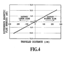
- FIG. 4 is a diagram showing relationships between the traveled distance ( ⁇ m) of the magnet versus difference magnetic flux density (mT) owing to the Hall elements in the subtraction method. Near the origin, the magnetic field becomes zero in terms of the sum. As the magnet moves from the origin, the magnitude of the magnetic field in terms of the sum increases linearly from left to right.
- FIG. 5A and FIG. 5B are diagrams for explaining the division method in the present invention: FIG. 5A shows relationships of the magnetic flux density (mT) against the traveled distance (mm); and FIG. 5B shows relationships of a magnetic flux density ratio against the traveled distance ( ⁇ m).
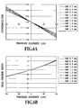
- FIG. 6A and FIG. 6B are diagrams showing the GAP dependence of the output signals in the position detecting sensors of the conventional difference (sum) method and of the division method in accordance with the present invention:
- FIG. 6A is a diagram showing the GAP dependence of the signal (difference/sum) in the difference (sum) method;
- FIG. 6B is a diagram showing the GAP dependence of the signal (absolute value of the ratio) in the division method.
- FIG. 6A and FIG. 6B show relationships between the traveled distance ( ⁇ m) and the output signals in the case where the distance between the centers of magneto-sensitive sections of the Hall elements 22a and 22b is 1 mm and where the GAP is varied from 0.7 mm to 1.5 mm.
- the difference/sum output of the Hall voltage in the range of ⁇ 100 ⁇ m from the origin (0 ⁇ m) has linear characteristics of declining from left to right as the movement from the minus to plus side.
- the output of the Hall voltage ratio in the range of ⁇ 100 ⁇ m from the origin (0 ⁇ m) has characteristics of increasing from left to right as the movement from the minus to plus side.
- the division method has an advantage that the output hardly fluctuates for the looseness in the vertical direction.
- FIG. 7 is a block diagram for explaining an embodiment of the position detecting device in accordance with the present invention, and is a diagram showing the signal processing circuit of the position detecting device when using the position detecting sensor in accordance with the division method shown in FIG. 3B .
- FIG. 7 is a block diagram for explaining an embodiment of the position detecting device in accordance with the present invention, and is a diagram showing the signal processing circuit of the position detecting device when using the position detecting sensor in accordance with the division method shown in FIG. 3B .
- the reference numeral 31 designates a multiplexer (MUX: selecting circuit), 32 designates a preamplifier (operational amplifier), 33 designates a clock signal generating circuit (Clock), 34 designates a sample and hold circuit (S/H), 3.5 designates a low-pass filter (LPF), 36 designates a feedback sample and hold circuit (FB S/H), 41 designates a PI (proportional-integral) regulator, 42 designates a reference voltage generating circuit, 43 - 45 each designate a resistance, 46 designates a capacitor, and 47 designates an operational amplifier.
- MUX multiplexer
- 32 designates a preamplifier (operational amplifier)
- 33 designates a clock signal generating circuit (Clock)
- 34 designates a sample and hold circuit (S/H)
- 3.5 designates a low-pass filter (LPF)
- 36 designates a feedback sample and hold circuit (FB S/H)
- 41 designates a PI (proportional-integral) regulator
- the MUX 31 is a selecting circuit with a function of selecting the signal component of the Hall element 22a (HE1) or the signal component of the Hall element 22b (HE2).
- the preamplifier 32 is an operational amplifier for amplifying the output voltages of the Hall elements 22a and 22b.
- the sample and hold circuit 34 is a circuit for sampling the signal from the preamplifier 32 in accordance with the clock signal the clock signal generating circuit 33 generates in response to the signal from the MUX 31.
- the low-pass filter 35 which is connected to the sample and hold circuit 34, outputs the position detection signal -Vref ⁇ B2/B1.
- the feedback sample and hold circuit 36 is a circuit for inputting the signal from the preamplifier 32 to the PI regulator 41.
- the PI regulator 41 comprises the reference voltage generating circuit 42, the resistances 43 to 45, the capacitor 46 and the operational amplifier 47.
- the operational amplifier 47 has its inverting input terminal connected to the feedback sample and hold circuit 36 via the resistance 44 and to the reference voltage generating circuit 42 via the resistance 43.
- the operational amplifier 47 has its non-inverting input terminal grounded.
- the operational amplifier 47 has the resistance 45 and capacitor 46 connected in series across its inverting input terminal and output terminal.
- the PI regulator 41 is a regulator for carrying out the PI control in such a manner that the signal sampled by the feedback sample and hold circuit 36 is adjusted to the voltage level of the reference voltage Vref.
- the PI regulator 41 performs the PI control according to the time constant determined by the resistance 45 and the capacitor 46 so that it can control the signal sampled discretely without oscillation.
- the clock signal generating circuit 33 is a circuit for generating the clock signal that determines the signal to be put into the sample and hold circuit 34 and the feedback sample and hold circuit 36.
- the PI regulator 41 supplies the Hall elements 22a and 22b with a driving current.
- the Hall voltage Vhe1 (Vhe2) output from the Hall element 22a (or 22b) is connected to the preamplifier 32 via the MUX 31 when the Hall element 22a (22b) is selected by the clock signal generated by the clock signal generating circuit 33, and is amplified at a prescribed amplification factor A.
- the Hall voltage Vhe1 of the Hall element 22a is amplified by the preamplifier 32 and is put into the PI regulator 41 via the feedback sample and hold circuit 36, and that the Hall voltage Vhe2 of the Hall element 22b is output via the sample and hold circuit 34 and low-pass filter 35.
- the Hall voltage Vhe1 of the Hall element 22a is amplified by the preamplifier 32 and becomes A ⁇ K ⁇ Bhe1 (where A is the amplification factor of the preamplifier 32, K is a constant, and Bhe1 is the magnetic flux density the Hall element 22a receives)
- the PI regulator 41 automatically varies the bias point of the PI output by the feedback control in such a manner as to satisfy the following expression.
- the Hall voltage Vhe2 of the Hall element 22b is given by the following expression. - Vref ⁇ Bhe ⁇ 2 / Bhe ⁇ 1
- the operation is performed by only the feedback control of the PI regulator 41, which means that the Hall voltage Vhe2 of the Hall element 22b output from the low-pass filter 35 is produced in the form of the ratio between the magnetic flux density of the Hall element 22a and that of the Hall element 22b without requiring any arithmetic means.
- the output voltage which is obtained by driving the Hall element 22b at the same voltage as the Hall element 22a while controlling the Hall voltage Vhe1 of the Hall element 22a at the constant voltage, has the form of dividing the magnetic flux density received by the Hall element 22b by that received by the Hall element 22a. Since the Hall voltage is proportional to the magnetic flux density, it is found that the foregoing expression (2) is equivalent to the division of the output voltage of the Hall element 22b by the output voltage of the Hall element 22a.
- the position detecting device in accordance with the present invention operates under the condition that the absolute value of the magnetic flux density detected by the Hall element 22a and Hall element 22b is a certain value excluding zero.
- the output voltage Vhe2 of the Hall element 22b is constant for temperature.
- the attenuation of the magnetic field is the same for Bhe1 and Bhe2, it does not have any effect on the output voltage Vhe2 of the Hall element 22b.
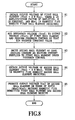
- FIG. 8 is a diagram showing a flowchart for explaining an embodiment of the position detecting method in accordance with the present invention.
- the amplified output voltage of the Hall element 22a is input to the PI regulator 41 via the feedback sample and hold circuit 36, and the PI regulator 41 adds the reference voltage (Vref) to the output voltage (Vhe1) of the Hall element 22a and carries out the feedback control in such a manner that its output becomes the constant value (step 2).
- the Hall element 22b is driven by the same driving current as the driving current supplied to the Hall element 22a under the feedback control (step 3).
- the amplified output voltage Vhe2 of the Hall element 22b is output in the form of the ratio (Bhe2/Bhe1) between the magnetic flux densities the Hall element 22a and Hall element 22b receive (step 5).
- the constant K is obtained from the output voltage of the first Hall element 22a, and the output of the magnetic flux density ratio Bhe2/Bhe1 is obtained from the relationships between the output voltage of the second Hall element 22b and the constant K
- the constant K can be obtained from the output voltage of the second Hall element 22b
- the output of the magnetic flux density ratio Bhe1/Bhe2 can be obtained from the relationships between the output voltage of the first Hall element 22a and the constant K.
- the foregoing embodiment is described by way of example having two Hall elements, it is obvious that it can be applied to the position detection having two or more Hall elements.
- the present invention which relates to a position detecting device and a position detecting method for detecting the origin of the autofocus or zoom position of a camera, can implement the position detecting device and the position detecting method that enable the cancellation of variation in the temperature characteristics and the elimination of an error owing to the looseness in the vertical direction by calculating the ratio between the output voltages of a plurality of Hall elements, and that enable miniaturization.
- the present invention employs the division method (ratio) so that the output at the origin becomes one (ratio) and the output at the time when the magnet is removed is zero, thereby being able to make the loaded or unloaded decision of the magnet.
Landscapes
- Physics & Mathematics (AREA)
- General Physics & Mathematics (AREA)
- Transmission And Conversion Of Sensor Element Output (AREA)
- Measurement Of Length, Angles, Or The Like Using Electric Or Magnetic Means (AREA)
- Lens Barrels (AREA)
Applications Claiming Priority (2)
| Application Number | Priority Date | Filing Date | Title |
|---|---|---|---|
| JP2006124224 | 2006-04-27 | ||
| PCT/JP2007/059114 WO2007126023A1 (fr) | 2006-04-27 | 2007-04-26 | Procédé et dispositif de détection de position |
Publications (2)
| Publication Number | Publication Date |
|---|---|
| EP2012094A1 true EP2012094A1 (fr) | 2009-01-07 |
| EP2012094A4 EP2012094A4 (fr) | 2013-07-31 |
Family
ID=38655547
Family Applications (1)
| Application Number | Title | Priority Date | Filing Date |
|---|---|---|---|
| EP07742549.4A Ceased EP2012094A4 (fr) | 2006-04-27 | 2007-04-26 | Procede et dispositif de detection de position |
Country Status (6)
| Country | Link |
|---|---|
| US (1) | US7818138B2 (fr) |
| EP (1) | EP2012094A4 (fr) |
| JP (2) | JP5051918B2 (fr) |
| KR (1) | KR101057951B1 (fr) |
| CN (1) | CN101432594B (fr) |
| WO (1) | WO2007126023A1 (fr) |
Cited By (2)
| Publication number | Priority date | Publication date | Assignee | Title |
|---|---|---|---|---|
| CN113219763A (zh) * | 2020-02-04 | 2021-08-06 | 三星电机株式会社 | 位置检测设备 |
| US11265482B2 (en) | 2019-12-27 | 2022-03-01 | Samsung Electro-Mechanics Co., Ltd. | Position detecting device of aperture module |
Families Citing this family (23)
| Publication number | Priority date | Publication date | Assignee | Title |
|---|---|---|---|---|
| JP5089999B2 (ja) * | 2007-01-24 | 2012-12-05 | オリンパス株式会社 | 位置検出回路及びその応用装置 |
| US7956604B2 (en) * | 2008-07-09 | 2011-06-07 | Infineon Technologies, Ag | Integrated sensor and magnetic field concentrator devices |
| KR101018798B1 (ko) | 2008-07-14 | 2011-03-03 | (주)모아린 | 물체 검출용 광학장치 |
| CN102789036A (zh) * | 2011-05-18 | 2012-11-21 | 亚洲光学股份有限公司 | 对焦机构 |
| US8717010B2 (en) * | 2011-08-19 | 2014-05-06 | Infineon Technologies Ag | Magnetic position sensors, systems and methods |
| JP5715023B2 (ja) * | 2011-10-12 | 2015-05-07 | 旭化成エレクトロニクス株式会社 | 位置検出装置及び位置検出方法並びにそれを用いた電子機器 |
| US9389247B2 (en) | 2011-11-04 | 2016-07-12 | Infineon Technologies Ag | Current sensors |
| JP5682798B2 (ja) * | 2012-08-06 | 2015-03-11 | 株式会社デンソー | 位置検出装置 |
| JP2014163691A (ja) * | 2013-02-21 | 2014-09-08 | Seiko Instruments Inc | 磁気センサ装置 |
| KR101588951B1 (ko) * | 2014-04-16 | 2016-01-26 | 삼성전기주식회사 | 보이스 코일 모터 액추에이터 구동 장치 |
| JP2016050841A (ja) * | 2014-08-29 | 2016-04-11 | 株式会社東海理化電機製作所 | 磁気検出装置 |
| JP6503735B2 (ja) | 2014-12-26 | 2019-04-24 | ミツミ電機株式会社 | レンズ駆動装置、カメラモジュール、及びカメラ搭載装置 |
| CN105865327A (zh) * | 2015-01-22 | 2016-08-17 | 成都飞机工业(集团)有限责任公司 | 基于变焦照片的相对位置的测量方法 |
| CN107923763B (zh) * | 2015-08-31 | 2020-11-06 | 日立汽车系统株式会社 | 位置传感器以及靶标 |
| JP6833204B2 (ja) * | 2016-02-25 | 2021-02-24 | セニス エージー | 磁界の角度を測定する角度センサ及び方法 |
| JP6934708B2 (ja) * | 2016-07-20 | 2021-09-15 | メレキシス テクノロジーズ エス エーMelexis Technologies SA | 変位検出装置 |
| CN106949822B (zh) * | 2017-01-24 | 2020-11-17 | 瑞声科技(新加坡)有限公司 | 微型器件的实时位移反馈系统及其反馈方法 |
| WO2019049652A1 (fr) | 2017-09-06 | 2019-03-14 | 株式会社村田製作所 | Dispositif de détection de déplacement |
| JP7194567B2 (ja) * | 2018-11-14 | 2022-12-22 | 旭化成エレクトロニクス株式会社 | カメラモジュール |
| CN110501797B (zh) * | 2019-09-20 | 2022-09-06 | 合肥英睿系统技术有限公司 | 一种可自动检测识别视场的红外镜头装置 |
| CN112325755A (zh) * | 2020-11-03 | 2021-02-05 | 上海艾为电子技术股份有限公司 | 一种位置传感系统、获取位置传感信号的方法及电子设备 |
| KR20230158195A (ko) * | 2022-05-11 | 2023-11-20 | 엘지이노텍 주식회사 | 카메라 모듈 및 이를 포함하는 광학기기 |
| CN115324946B (zh) * | 2022-10-11 | 2022-12-16 | 恒天益科技(深圳)有限公司 | 一种抽气量控制方法、装置及终端 |
Family Cites Families (21)
| Publication number | Priority date | Publication date | Assignee | Title |
|---|---|---|---|---|
| JP2570654B2 (ja) | 1987-12-08 | 1997-01-08 | 日本精工株式会社 | 変位検出装置 |
| US4970463A (en) * | 1989-03-13 | 1990-11-13 | Durakool Incorporated | Temperature stable proximity sensor with sensing of flux emanating from the lateral surface of a magnet |
| JPH05333048A (ja) * | 1992-06-02 | 1993-12-17 | Fujitsu Ltd | 磁気加速度センサ |
| JP3318045B2 (ja) * | 1993-05-28 | 2002-08-26 | オリンパス光学工業株式会社 | 落射蛍光顕微鏡 |
| US5932984A (en) * | 1995-09-04 | 1999-08-03 | Canon Kabushiki Kaisha | Driving apparatus and optical apparatus |
| JPH09231889A (ja) * | 1996-02-26 | 1997-09-05 | Matsushita Electric Works Ltd | 位置検出センサ |
| JPH11120733A (ja) * | 1997-10-17 | 1999-04-30 | Sony Corp | ディスクカートリッジおよびディスクドライブ装置 |
| JP4378814B2 (ja) * | 1999-07-16 | 2009-12-09 | 株式会社日本自動車部品総合研究所 | 回転角検出装置 |
| JP2001050956A (ja) * | 1999-08-05 | 2001-02-23 | Matsushita Electric Ind Co Ltd | 尿検査装置 |
| JP2001091298A (ja) * | 1999-09-21 | 2001-04-06 | Sumitomo Metal Mining Co Ltd | 非接触磁気式計測装置 |
| JP2002054903A (ja) * | 2000-08-10 | 2002-02-20 | Nippon Densan Corp | 変位検出装置 |
| EP1243897B1 (fr) * | 2001-03-23 | 2013-12-18 | Melexis Technologies NV | Capteur de position magnétique |
| KR100564866B1 (ko) * | 2002-03-22 | 2006-03-28 | 아사히 가세이 일렉트로닉스 가부시끼가이샤 | 각도 검출 장치 및 각도 검출 시스템 |
| JP2003344187A (ja) * | 2002-05-31 | 2003-12-03 | Kayaba Ind Co Ltd | トルク検出機構 |
| JP3967660B2 (ja) | 2002-10-09 | 2007-08-29 | ペンタックス株式会社 | 移動部材の原点位置検出機構 |
| WO2005033716A1 (fr) * | 2003-10-01 | 2005-04-14 | Eaton Corporation | Systeme et procede de detection de courant faisant appel a la detection de courant anti-differentielle et a correction d'erreurs |
| JP4729885B2 (ja) | 2004-07-20 | 2011-07-20 | パナソニック株式会社 | 撮像装置 |
| JP2005284169A (ja) | 2004-03-30 | 2005-10-13 | Konica Minolta Opto Inc | 駆動装置及び光学機器 |
| JP4049125B2 (ja) | 2004-05-20 | 2008-02-20 | コニカミノルタオプト株式会社 | 位置検出装置、手振れ補正機構、および撮像装置 |
| JP2006047054A (ja) | 2004-08-03 | 2006-02-16 | Konica Minolta Photo Imaging Inc | 位置検出装置、手ぶれ補正装置および撮像装置 |
| JP2006044448A (ja) * | 2004-08-04 | 2006-02-16 | Toyota Motor Corp | 車輪情報認識システム及び車体側車輪情報認識装置、車輪側車輪情報認識装置 |
-
2007
- 2007-04-26 US US12/298,445 patent/US7818138B2/en active Active
- 2007-04-26 EP EP07742549.4A patent/EP2012094A4/fr not_active Ceased
- 2007-04-26 KR KR1020087025959A patent/KR101057951B1/ko not_active Expired - Fee Related
- 2007-04-26 JP JP2008513274A patent/JP5051918B2/ja not_active Expired - Fee Related
- 2007-04-26 CN CN2007800149546A patent/CN101432594B/zh not_active Expired - Fee Related
- 2007-04-26 WO PCT/JP2007/059114 patent/WO2007126023A1/fr not_active Ceased
-
2012
- 2012-06-26 JP JP2012143434A patent/JP5735459B2/ja not_active Expired - Fee Related
Cited By (2)
| Publication number | Priority date | Publication date | Assignee | Title |
|---|---|---|---|---|
| US11265482B2 (en) | 2019-12-27 | 2022-03-01 | Samsung Electro-Mechanics Co., Ltd. | Position detecting device of aperture module |
| CN113219763A (zh) * | 2020-02-04 | 2021-08-06 | 三星电机株式会社 | 位置检测设备 |
Also Published As
| Publication number | Publication date |
|---|---|
| CN101432594B (zh) | 2011-02-16 |
| CN101432594A (zh) | 2009-05-13 |
| JP2012189613A (ja) | 2012-10-04 |
| US20090177436A1 (en) | 2009-07-09 |
| EP2012094A4 (fr) | 2013-07-31 |
| JP5051918B2 (ja) | 2012-10-17 |
| JPWO2007126023A1 (ja) | 2009-09-10 |
| US7818138B2 (en) | 2010-10-19 |
| WO2007126023A1 (fr) | 2007-11-08 |
| JP5735459B2 (ja) | 2015-06-17 |
| KR20090006117A (ko) | 2009-01-14 |
| KR101057951B1 (ko) | 2011-08-18 |
Similar Documents
| Publication | Publication Date | Title |
|---|---|---|
| EP2012094A1 (fr) | Procede et dispositif de detection de position | |
| JP5715023B2 (ja) | 位置検出装置及び位置検出方法並びにそれを用いた電子機器 | |
| KR101588951B1 (ko) | 보이스 코일 모터 액추에이터 구동 장치 | |
| JP5089999B2 (ja) | 位置検出回路及びその応用装置 | |
| US7315164B2 (en) | Drive unit provided with position detecting device | |
| US5932984A (en) | Driving apparatus and optical apparatus | |
| EP2015034B1 (fr) | Débitmètre de type Coriolis avec détecteur optique de vibrations | |
| US8509611B2 (en) | Lens controlling device and imaging apparatus using the same | |
| TWI461649B (zh) | 使用反射型光感測器之位置檢測裝置 | |
| KR20180115959A (ko) | 홀센서의 출력전압을 교정하여 렌즈위치를 검출하는 렌즈위치 검출장치 | |
| US7856126B2 (en) | Position sensing device | |
| US7405750B2 (en) | Position-detecting apparatus | |
| KR101625098B1 (ko) | 휴대폰 카메라의 액츄에이터 측정시스템 | |
| JP2017106954A (ja) | レンズ装置、カメラ本体および光学機器 | |
| CN113316708B (zh) | 位置检测装置 | |
| JP5345305B2 (ja) | 撮影装置及び撮影方法 | |
| US7885534B2 (en) | Light-amount adjusting system and optical apparatus | |
| JP2010038597A (ja) | 磁気利用の位置検出方法及び位置検出センサ | |
| KR100247766B1 (ko) | 비디오 카메라의 리니어모터 위치검출장치 | |
| JP2008180561A (ja) | 位置検出回路及び撮像装置 | |
| KR101742620B1 (ko) | 휴대폰 카메라의 액츄에이터 측정시스템 | |
| KR20220032754A (ko) | 렌즈구동 액츄에이터 | |
| JPH04217215A (ja) | レンズ位置検出装置 |
Legal Events
| Date | Code | Title | Description |
|---|---|---|---|
| PUAI | Public reference made under article 153(3) epc to a published international application that has entered the european phase |
Free format text: ORIGINAL CODE: 0009012 |
|
| 17P | Request for examination filed |
Effective date: 20081030 |
|
| AK | Designated contracting states |
Kind code of ref document: A1 Designated state(s): AT BE BG CH CY CZ DE DK EE ES FI FR GB GR HU IE IS IT LI LT LU LV MC MT NL PL PT RO SE SI SK TR |
|
| AX | Request for extension of the european patent |
Extension state: AL BA HR MK RS |
|
| DAX | Request for extension of the european patent (deleted) | ||
| RBV | Designated contracting states (corrected) |
Designated state(s): DE |
|
| A4 | Supplementary search report drawn up and despatched |
Effective date: 20130701 |
|
| RIC1 | Information provided on ipc code assigned before grant |
Ipc: G03B 13/36 20060101ALI20130625BHEP Ipc: G01D 5/14 20060101AFI20130625BHEP |
|
| STAA | Information on the status of an ep patent application or granted ep patent |
Free format text: STATUS: EXAMINATION IS IN PROGRESS |
|
| 17Q | First examination report despatched |
Effective date: 20170613 |
|
| REG | Reference to a national code |
Ref country code: DE Ref legal event code: R003 |
|
| RIN1 | Information on inventor provided before grant (corrected) |
Inventor name: SUZUKI, MASARU Inventor name: YOSHIDA, TAKASHI Inventor name: KAKUTA, KATSUMI |
|
| STAA | Information on the status of an ep patent application or granted ep patent |
Free format text: STATUS: THE APPLICATION HAS BEEN REFUSED |
|
| 18R | Application refused |
Effective date: 20200326 |