EP2013956B1 - Circuit regenerateur de commande de grille d'un mosfet de puissance - Google Patents
Circuit regenerateur de commande de grille d'un mosfet de puissance Download PDFInfo
- Publication number
- EP2013956B1 EP2013956B1 EP20070809031 EP07809031A EP2013956B1 EP 2013956 B1 EP2013956 B1 EP 2013956B1 EP 20070809031 EP20070809031 EP 20070809031 EP 07809031 A EP07809031 A EP 07809031A EP 2013956 B1 EP2013956 B1 EP 2013956B1
- Authority
- EP
- European Patent Office
- Prior art keywords
- switching device
- gate
- winding
- coupled
- mosfet
- Prior art date
- Legal status (The legal status is an assumption and is not a legal conclusion. Google has not performed a legal analysis and makes no representation as to the accuracy of the status listed.)
- Ceased
Links
Images



Classifications
-
- H—ELECTRICITY
- H03—ELECTRONIC CIRCUITRY
- H03K—PULSE TECHNIQUE
- H03K17/00—Electronic switching or gating, i.e. not by contact-making and –breaking
- H03K17/16—Modifications for eliminating interference voltages or currents
- H03K17/161—Modifications for eliminating interference voltages or currents in field-effect transistor switches
- H03K17/162—Modifications for eliminating interference voltages or currents in field-effect transistor switches without feedback from the output circuit to the control circuit
-
- H—ELECTRICITY
- H02—GENERATION; CONVERSION OR DISTRIBUTION OF ELECTRIC POWER
- H02M—APPARATUS FOR CONVERSION BETWEEN AC AND AC, BETWEEN AC AND DC, OR BETWEEN DC AND DC, AND FOR USE WITH MAINS OR SIMILAR POWER SUPPLY SYSTEMS; CONVERSION OF DC OR AC INPUT POWER INTO SURGE OUTPUT POWER; CONTROL OR REGULATION THEREOF
- H02M1/00—Details of apparatus for conversion
- H02M1/08—Circuits specially adapted for the generation of control voltages for semiconductor devices incorporated in static converters
- H02M1/088—Circuits specially adapted for the generation of control voltages for semiconductor devices incorporated in static converters for the simultaneous control of series or parallel connected semiconductor devices
-
- H—ELECTRICITY
- H03—ELECTRONIC CIRCUITRY
- H03K—PULSE TECHNIQUE
- H03K17/00—Electronic switching or gating, i.e. not by contact-making and –breaking
- H03K17/04—Modifications for accelerating switching
- H03K17/041—Modifications for accelerating switching without feedback from the output circuit to the control circuit
- H03K17/0412—Modifications for accelerating switching without feedback from the output circuit to the control circuit by measures taken in the control circuit
- H03K17/04123—Modifications for accelerating switching without feedback from the output circuit to the control circuit by measures taken in the control circuit in field-effect transistor switches
-
- H—ELECTRICITY
- H03—ELECTRONIC CIRCUITRY
- H03K—PULSE TECHNIQUE
- H03K2217/00—Indexing scheme related to electronic switching or gating, i.e. not by contact-making or -breaking covered by H03K17/00
- H03K2217/0036—Means reducing energy consumption
Definitions
- This invention relates generally to switched mode power converters and in particular to a regenerative gate drive circuit for voltage control of MOSFETs (Metal Oxide Silicon Field Effect Switching device) and IGBT (Insulated Gate Bipolar Switching device) having means for recovering energy stored in the gate capacitance and means for speeding up gate voltage transitions and reducing output impedance.
- MOSFETs Metal Oxide Silicon Field Effect Switching device
- IGBT Insulated Gate Bipolar Switching device
- Fig. 1 As conventional prior art gate drive circuit is shown in Fig. 1 comprising a totem pole pair of field effect switching devices Q1 and Q2 and a gate resistor, R g .
- This topology suffers from excessive power dissipation particularly at high frequency.
- the three major sources of power dissipation are as follows: 1. capacitive energy losses, 2. cross conduction power losses, and 3. linear operation losses.
- U.S. Patent No. 5,264,736 issued November 23, 1993 to B. Jacobson discloses a high frequency resonant gate drive for a Power MOSFET. This regenerative topology enables partial energy recovery and protects against cross-conduction. It also provides low output impedance because currents circulate in clamp diodes during the time interval between the gate voltage transitions. However, energy recovery takes place only during the narrow time interval prior to the turn off of the main switching device when voltage across the resonant inductor exceeds the bias supply.
- U.S. Patent No. 6,208,535 issued March 27, 2001 to David Parks discloses a resonant gate driver that provides a resonant switching for a field effect transistor (FET) and associated circuits such as power supplies with synchronous output rectifiers.
- FET field effect transistor
- the resonant switching for a junction FET invokes bipolar mode operation with a diode clamping of the gate, which results in bipolar mode operation without a separate bias power supply.
- this resonant gate driver does not provide energy recovery for efficiency improvement.
- a regenerative gate drive circuit comprising a positive power source coupled to a first switching device, a negative power source coupled to a second switching device, a first inductor network comprises a first winding and a second winding on each side of a center tap, said center tap being coupled to a gate input of a power MOSFET, a second inductor network comprises a first winding in series with a first blocking capacitor and a second winding in series with a second blocking capacitor on each side of a center tap, the center tap being coupled to the gate input of a power MOSFET and to the center tap of the first inductor network, the first switching device, coupled between the positive power source and the first winding of the first inductor network in parallel with the first blocking capacitor in series with the first winding of the second inductor network, provides a path for a first current to flow through the first switching device and the first winding of the first inductor network in parallel with the first winding of the second inductor which is in series with
- Each of the first switching device and the second switching device comprises a MOSFET.
- the first input signal is coupled to an input gate of the first MOSFET
- second input signal is coupled to an input gate of the second MOSFET.
- the first winding and the second winding of the first inductor network and the second inductor network comprises an equal number of turns.
- the second limiting means comprises a first diode coupled between the positive power source and the second switching device and a second diode coupled between the negative power source and the first switching device.
- the second inductor network provides reduced output impedance thereby improving noise immunity.
- the first inductor network and the second inductor network provide a high impedance between the first switching device and the second switching device when the switching devices are both conducting simultaneously.
- the circuit provides a dead time interval when the first input signal and the second input signal are at a level that turns-off the first switching device and the second switching device thereby enabling energy recovery.
- Control of the dead time interval is provided by means for sensing any one of an output voltage or output current of the power MOSFET, or power across the power MOSFET or temperature at a junction of the power MOSFET.
- a method for providing a regenerative gate drive circuit comprising the steps of providing a positive power source coupled to a first switching device, providing a negative power source coupled to a second switching device, providing a first inductor network having a first winding and a second winding on each side of a center tap, said center tap being coupled to a gate input of a power MOSFET, providing a second inductor network having a first winding in series with a first blocking capacitor and a second winding in series with a second blocking capacitor on each side of a center tap, the center tap being coupled to the gate input of a power MOSFET and to the center of tap of the first inductor network, providing a path for a first current to flow through the first switching device and the first winding of the first inductor network in parallel with the first winding of the second inductor which is in series with the first blocking capacitor, the first switching device being coupled between the positive power source and the first winding of the first inductor network in parallel with the first blocking capacitor
- the method includes the step of providing a MOSFET for each of the first switching device and the second switching device.
- the method comprises the steps of coupling the first input signal to an input gate of the first MOSFET, and coupling the second input signal to an input gate of the second MOSFET.
- the method further comprises the step of providing the first winding and the second winding of the first inductor network and the second inductor network with an equal number of turns.
- the step of limiting the voltage of the gate of the power MOSFET comprises the steps of providing a first diode coupled between the positive power source and the second switching device, and providing a second diode coupled between the negative power source and the first switching device.
- the regenerative gate drive circuit 10 comprises a pair of MOSFET (metal oxide silicon field effect switching) devices Q1, Q2 connected in a series with coupled inductors L1, L2 between them, the coupled inductors having a center tap 25 which is connected to a gate of a power MOSFET 38.
- the coupled inductors L1, L2 comprise an upper half winding and a lower half winding each having an inductance of 300 mH with an inductor coupling factor (k) of 0.92.
- Coupled in parallel with the main coupled inductors L1, L2 are coupled inductors L3, L4 with an inductor coupling factor (k) of 0.92 and blocking capacitators C1, C2.
- Blocking capacitor C1 is connected in series with inductor L3 and another blocking capacitator C2 is connected in series with inductor L4.
- the center tap 27 of coupled inductor L3, L4 connects to the center tap 25 of L1 and L2.
- a power or voltage source V dd has a positive terminal connected to a drain terminal of MOSFET Q1 and has a negative terminal connected to a positive terminal of voltage source V ss .
- the negative terminal of V ss connects to the source of MOSFET Q2.
- Two clamping diodes D1, D2 are provided wherein diode D1 is connected from the voltage source V dd to the drain of MOSFET Q2, and diode D2 is connected from the voltage source V ss to the source of MOSFET Q1.
- V dd provides 12.6 volts DC and V ss provides 5 volts DC.
- FIG. 3 is a graph of typical voltage and current waveforms at the gates of MOSFETS Q1 and Q2 and typical waveforms of the current through coupled inductors L1 and L2 and coupled inductors L3 and L4.
- FIG. 4 is a graph showing typical current waveforms through the voltage sources V ss and V ss , diodes D1 and D2, and MOSFET switching devices Q1 and Q2.
- the gate signal V gate Q2 provided by signal VG2 for the switching device Q2 is switched off (low) and it starts turning-off.
- Switching device Q1 is not turned-on yet, so the switching cycle begins with a dead time interval 41 when gate signals V gate Q1 and V gate Q2 to both switching devices are off.
- output of the gate driver 10 gate voltage of the power MOSFET 38
- diode D1 is off
- diode D2 conducts current through inductors L1, L2, and Q2.
- Q2 turns off, its voltage begins to rise and current in the inductor L2 diverts to the inductor L4.
- the dead time interval 41 ends at t ⁇ 50 ns when the gate signal V gate Q1 from VG1 starts turning on switching device Q1.
- the voltage is applied to the coupled inductors L1, L2 and L3, L4 and the power MOSFET 38 gate is resonantly charged by the sum of two currents.
- the source V dd generates the first current that flows through Q1 and L1 in parallel with L3.
- the second current is the one that was stored in L2 and L4 and it flows through the integral body diode of the switching device Q2 returning energy to the source V ss .
- the resonant gate drive circuit 10 has such non-linear elements as the power MOSFET 38 gate and reverse transfer capacitance, it is exceedingly difficult to obtain a closed form solution for its voltages and currents.
- the next time interval begins when the power MOSFET 38 starts turning-on at t ⁇ 100 ns.
- drain voltage of the switching device Q2 changes and becomes negative while current through Q2 approaches zero. Since currents in the inductors L2 and L4 pass through Q2 and can not disappear, the summary current I L2 + I L4 begins flowing through the diode D1 thereby returning energy stored in the inductors L2 and L4 to the power source V dd .
- the gate drive current 10 begins recharging its reverse transfer ("Miller") capacitance. A major part of this current comes from the source V dd through the inductors L1 and L3. The recharging of the Miller capacitance also causes a dip in the power MOSFET 38 gate voltage waveform V gate 44.
- the turn-off processes are similar to the ones that take place during the turn-on interval.
- the gate signal v gate Q1 from VG1 for the switching device Q1 is switched-off, and it starts turning-off.
- the switching device Q2 is not turned-on yet, so the turn-off interval begins with another "dread time" interval 43 when gate signals to both switching devices Q1 and Q2 are off.
- the output of the gate drive circuit 10 (to the power MOSFET 38 gate) is positive, D2 is off, and D1 conducts current through inductors L1, L2, and Q1.
- the dead time interval 43 ends at t ⁇ 550 ns when the gate signal V gate Q2 from VG2 starts turning-on the switching device Q2.
- the voltage is applied to the coupled inductors L1, L2 and L3, L4 and the power MOSFET 38 gate is resonantly discharged by the sum of two currents.
- the source voltage V ss generates the first current that flows through Q2 and L2 in parallel with L4.
- the second current is the one that is stored in inductors L1 and L3, and it flows through the integral body diode of the switching device Q1 returning energy to the source V dd .
- the next time interval begins when the power MOSFET 38 starts turning off at t ⁇ 600 ns.
- drain voltage of the switching device Q1 turns negative and its current declines. Since currents in the inductors L1 and L3 flowing through Q1 can not disappear, the summary current I L1 + I L3 flows through the diode D2 thereby returning energy stored in the inductors L1 and L3 to the power source V ss .
- the gate drive current begins recharging its reverse transfer (“Miller") capacitance. A major part of this current comes from the voltage source V ss through the inductors L2 and L4. The recharging of the Miller capacitance also causes a dip in MOSFET gate voltage waveform V gate 44.
- the energy regenerative gate drive circuit 10 has positive and negative voltage sources V dd , V ss .
- the negative source V ss improves noise immunity of the gate drive circuit 10 by developing negative voltage across the power MOSFET 38 gate during the off time. Both voltage sources take part in energy recovery wherein during turn-on of the MOSFET, energy is returned to the negative voltage source V ss , and during turn-off it is returned to the positive voltage source V dd . Therefore, the efficiency of the regenerative gate drive circuit 10 is improved.
- gate capacitance of the power MOSFET 38 is partially discharged prior to on-to-off and off-to-on transitions thereby speeding up both switching transitions compared to the circuit disclosed in U.S. Patent 5,264,736 .
- the partial discharge represents MOSFET gate energy recovery through clamp diodes D1 and D2 and resonant inductors L1, L2 and L3, L4.
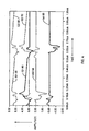
- FIG. 5 is a graph showing a measured power MOSFET 38 gate voltage relative to input gate signal VG1 generated by prior art gate drive circuit of FIG. 1
- FIG. 6 is a graph showing a measured power MOSFET 38 gate voltage relative to the input gate signal VG1, generated by the regenerative gate drive circuit 10 of FIG. 2
- the LLCC network 33 comprised of coupled inductors L3, L4 and capacitors C1, C2 speed-up charging and discharging power MOSFET 38 that is critically important to reducing switching losses.
- the conventional gate driver disclosed in U.S. Patent 5,264,736 has slower transitions.
- the LLCC network 33 also reduces the output impedance of the gate driver circuit 10 thereby improving its noise immunity, and it reduces the linear operation losses of the gate driver circuit 10 because gate drive switching devices Q1 and Q2 are decoupled from the power MOSFET 38 gate capacitance.
- the prior art conventional gate driver of FIG. 1 has 33% higher power consumption than that of the gate driver circuit 10 of FIG. 2 . This was determined by averaging measurements of four prototypes of the gate driver circuit 10 at 750 kHz switching frequency.
Landscapes
- Engineering & Computer Science (AREA)
- Power Engineering (AREA)
- Power Conversion In General (AREA)
- Electronic Switches (AREA)
- Dc-Dc Converters (AREA)
Claims (14)
- Circuit régénérateur d'attaque de grille comprenant :une source d'alimentation positive (Vdd) reliée à un premier dispositif de commutation (Q1) ;une source d'alimentation négative (Vss) reliée à un second dispositif de commutation (Q2) ;un premier réseau d'inductances comprenant un premier enroulement (L1) et un second enroulement (L2) de chaque côté d'une dérivation centrale (25), ladite dérivation centrale étant reliée à une entrée de grille d'un MOSFET de puissance ;un second réseau d'inductances comprenant un premier enroulement (L3) en série avec un premier condensateur de blocage (C1) et un second enroulement (L4) en série avec un second condensateur de blocage (C2) de chaque côté d'une dérivation centrale (27), ladite dérivation centrale étant reliée à ladite entrée de grille d'un MOSFET de puissance et à ladite dérivation centrale (25) dudit premier réseau d'inductances ;ledit premier dispositif de commutation (Q1) étant relié entre ladite source d'alimentation positive (Vdd) et ledit premier enroulement (L1) dudit premier réseau d'inductances qui est en parallèle avec ledit premier condensateur de blocage (C1) en série avec ledit premier enroulement (L3) dudit second réseau d'inductances, pour former un trajet destiné au passage d'un premier courant à travers ledit premier dispositif de commutation (Q1) et ledit premier enroulement (L1) dudit premier réseau d'inductances qui est en parallèle avec ledit premier enroulement (L3) dudit second réseau d'inductances qui est en série avec ledit premier condensateur de blocage (C1) ;ledit second dispositif de commutation (Q2) étant relié entre ladite source d'alimentation négative (Vss) et ledit second enroulement (L2) dudit premier réseau d'inductances qui est en parallèle avec ledit second enroulement (L4) dudit second réseau d'inductances, ledit second enroulement étant en série avec un second condensateur de blocage (C2), pour former un trajet destiné à une décharge raisonnante dudit MOSFET de puissance ;un premier signal d'entrée (VG1) relié à une grille dudit premier dispositif de commutation pour commander ledit premier dispositif de commutation ;un second signal d'entrée (VG2) relié à une grille dudit second dispositif de commutation pour commander ledit second dispositif de commutation ;un premier moyen relié audit premier dispositif de commutation et audit second dispositif de commutation pour limiter la tension fournie à la grille dudit MOSFET de puissance et pour conduire un courant d'induction ; etun second moyen (D1, D2) relié entre ladite source d'alimentation positive et ledit second dispositif de commutation et entre ladite source d'alimentation négative et ledit premier dispositif de commutation pour limiter la tension sur la grille dudit MOSFET de puissance et pour conduire un courant d'induction.
- Circuit régénérateur d'attaque de grille selon la revendication 1, dans lequel : chacun dudit premier dispositif de commutation et dudit second dispositif de commutation comprend un MOSFET.
- Circuit régénérateur d'attaque de grille selon la revendication 2, dans lequel : ledit premier signal d'entrée est relié à une grille d'entrée dudit premier MOSFET, et ledit second signal d'entrée est relié à une grille d'entrée dudit second MOSFET.
- Circuit régénérateur d'attaque de grille selon la revendication 1, dans lequel : ledit premier enroulement et ledit second enroulement dudit premier réseau d'inductances et dudit second réseau d'inductances comprennent un même nombre de spires.
- Circuit régénérateur d'attaque de grille selon la revendication 1, dans lequel : ledit second moyen de limitation comprend une première diode (D1) reliée entre ladite source d'alimentation positive et ledit second dispositif de commutation et une seconde diode (D2) reliée entre ladite source d'alimentation négative et ledit premier dispositif de commutation.
- Circuit régénérateur d'attaque de grille selon la revendication 1, dans lequel ledit second réseau d'inductances fournit une impédance de sortie réduite pour ainsi améliorer l'immunité au bruit.
- Circuit régénérateur d'attaque de grille selon la revendication 1, dans lequel ledit premier réseau d'inductances et ledit second réseau d'inductances fournissent une haute impédance entre ledit premier dispositif de commutation et ledit second dispositif de commutation lorsque lesdits dispositifs de commutation sont tous deux simultanément conducteurs.
- Circuit régénérateur d'attaque de grille selon la revendication 1, dans lequel ledit circuit fournit un intervalle de temps mort lorsque ledit premier signal d'entrée et ledit second signal d'entrée sont à un niveau qui rend non passant ledit premier dispositif de commutation et ledit second dispositif de commutation pour ainsi permettre une récupération d'énergie.
- Circuit régénérateur d'attaque de grille selon la revendication 8, dans lequel la commande dudit intervalle de temps mort est assurée par un moyen destiné à détecter l'une quelconque d'une tension de sortie ou d'un courant de sortie dudit MOSFET de puissance, ou d'une puissance aux bornes dudit MOSFET de puissance ou d'une température au niveau d'une jonction dudit MOSFET de puissance.
- Procédé de fourniture d'un circuit régénérateur d'attaque de grille comprenant les étapes consistant à :fournir une source d'alimentation positive (Vdd) reliée à un premier dispositif de commutation (Q1) ;fournir une source d'alimentation négative (Vss) reliée à un second dispositif de commutation (Q2) ;fournir un premier réseau d'inductances comprenant un premier enroulement (L1) et un second enroulement (L2) de chaque côté d'une dérivation centrale (25), ladite dérivation centrale étant reliée à une entrée de grille d'un MOSFET de puissance ;fournir un second réseau d'inductances comprenant un premier enroulement (L3) en série avec un premier condensateur de blocage (C3) et un second enroulement (L4) en série avec un second condensateur de blocage (C2) de chaque côté d'une dérivation centrale (27), ladite dérivation centrale étant reliée à ladite entrée de grille d'un MOSFET de puissance et à ladite dérivation centrale (25) du premier réseau d'inductances ;former un trajet destiné au passage d'un premier courant à travers ledit premier dispositif de commutation (Q1) et ledit premier enroulement (L1) dudit premier réseau d'inductances qui est en parallèle avec ledit premier enroulement (L3) de ladite seconde inductance qui est en série avec ledit premier condensateur de blocage (C1), ledit premier dispositif de commutation étant relié entre ladite source d'alimentation positive (Vdd) et ledit premier enroulement (L1) dudit premier réseau d'inductances qui est en parallèle avec ledit premier condensateur de blocage (C1) qui est en série avec ledit premier enroulement (L3) dudit second réseau d'inductances ;former un trajet qui est destiné à la décharge résonante dudit MOSFET de puissance à travers ledit second dispositif de commutation (Q2) relié entre ladite source d'alimentation négative (Vss) et ledit second enroulement (L2) dudit premier réseau d'inductances qui est en parallèle avec ledit second enroulement (L4) dudit second réseau d'inductances, ledit second enroulement étant en série avec un second condensateur de blocage (C2) ;commander ledit premier dispositif de commutation au moyen d'un premier signal d'entrée (VG1) relié à une grille dudit premier dispositif de commutation ;commander ledit second dispositif de commutation au moyen d'un second signal d'entrée (VG2) relié à une grille dudit second dispositif de commutation ;limiter la tension fournie sur la grille dudit MOSFET de puissance et conduire un courant d'induction à l'aide d'un moyen relié au premier dispositif de commutation et audit second dispositif de commutation ; etlimiter la tension fournie sur la grille dudit MOSFET de puissance et conduire un courant d'induction à l'aide d'un moyen (D1, D2) relié entre ladite source d'alimentation positive et ledit second dispositif de commutation et entre ladite source d'alimentation négative et ledit premier dispositif de commutation.
- Procédé selon la revendication 10, comprenant l'étape consistant à fournir un MOSFET pour chacun dudit premier dispositif de commutation et dudit second dispositif de commutation.
- Procédé selon la revendication 11, dans lequel ledit procédé comprend les étapes consistant à : relier ledit premier signal d'entrée à une grille d'entrée dudit premier MOSFET ; et
relier ledit second signal d'entrée à une grille d'entrée dudit second MOSFET. - Procédé selon la revendication 10, dans lequel ledit procédé comprend l'étape consistant à conférer audit premier enroulement et audit second enroulement dudit premier réseau d'inductances et dudit second réseau d'inductances un même nombre de spires.
- Procédé selon la revendication 10, dans lequel ladite seconde étape de limitation de la tension de la grille dudit MOSFET de puissance comprend les étapes consistant à :fournir une première diode (D1) reliée entre ladite source d'alimentation positive et ledit second dispositif de commutation ; etfournir une seconde diode (D2) reliée entre ladite source d'alimentation négative et ledit premier dispositif de commutation.
Applications Claiming Priority (2)
| Application Number | Priority Date | Filing Date | Title |
|---|---|---|---|
| US11/415,756 US7285876B1 (en) | 2006-05-01 | 2006-05-01 | Regenerative gate drive circuit for power MOSFET |
| PCT/US2007/010251 WO2007127378A2 (fr) | 2006-05-01 | 2007-04-27 | Circuit régénérateur de commande de grille d'un mosfet d'et puissance |
Publications (3)
| Publication Number | Publication Date |
|---|---|
| EP2013956A2 EP2013956A2 (fr) | 2009-01-14 |
| EP2013956A4 EP2013956A4 (fr) | 2010-10-13 |
| EP2013956B1 true EP2013956B1 (fr) | 2011-11-02 |
Family
ID=38607016
Family Applications (1)
| Application Number | Title | Priority Date | Filing Date |
|---|---|---|---|
| EP20070809031 Ceased EP2013956B1 (fr) | 2006-05-01 | 2007-04-27 | Circuit regenerateur de commande de grille d'un mosfet de puissance |
Country Status (5)
| Country | Link |
|---|---|
| US (1) | US7285876B1 (fr) |
| EP (1) | EP2013956B1 (fr) |
| JP (1) | JP4880751B2 (fr) |
| AT (1) | ATE532263T1 (fr) |
| WO (1) | WO2007127378A2 (fr) |
Families Citing this family (17)
| Publication number | Priority date | Publication date | Assignee | Title |
|---|---|---|---|---|
| US8985850B1 (en) | 2009-10-30 | 2015-03-24 | Cypress Semiconductor Corporation | Adaptive gate driver strength control |
| AR080428A1 (es) | 2010-01-20 | 2012-04-11 | Chugai Pharmaceutical Co Ltd | Formulaciones liquidas estabilizadas contentivas de anticuerpos |
| WO2012030867A2 (fr) * | 2010-08-30 | 2012-03-08 | The Trustees Of Dartmouth College | Circuit d'excitation de base à haut rendement pour transistors de puissance bipolaires à jonctions |
| US8847631B2 (en) | 2011-12-23 | 2014-09-30 | General Electric Company | High speed low loss gate drive circuit |
| EP2749442A3 (fr) | 2012-08-12 | 2014-09-24 | Richter, Berta | Système d'électromobilité de véhicule routier |
| US20150214830A1 (en) * | 2014-01-24 | 2015-07-30 | General Electric Company | System and method of power conversion |
| CN107210737B (zh) * | 2015-02-16 | 2020-07-31 | 爱信艾达株式会社 | 开关元件驱动电路 |
| US9755636B2 (en) | 2015-06-23 | 2017-09-05 | Microsoft Technology Licensing, Llc | Insulated gate device discharging |
| US10511218B2 (en) * | 2015-12-22 | 2019-12-17 | Mitsubishi Electric Corporation | Gate drive circuit, that supplies power to a gate of a semiconductor switching element, and carries out a driving on and off of the gate |
| EP3220546A1 (fr) | 2016-03-18 | 2017-09-20 | Neumüller Elektronik GmbH | Circuit de commande électronique et procédé d'exploitation pour au moins un transistor mosfet de puissance |
| JP6812912B2 (ja) * | 2017-06-26 | 2021-01-13 | Tdk株式会社 | Fet駆動回路 |
| US10250249B1 (en) | 2017-06-30 | 2019-04-02 | Bel Power Solutions Inc. | Recuperative gate drive circuit and method |
| EP3739755B1 (fr) | 2019-05-16 | 2025-07-02 | Solaredge Technologies Ltd. | Circuit d'attaque de grille pour commutation fiable |
| CN111355361B (zh) * | 2020-01-09 | 2021-05-25 | 南京航空航天大学 | 一种实现eGaN HEMT并联动态均流的耦合电感栅极驱动电路 |
| CN112491251B (zh) * | 2020-12-09 | 2021-12-03 | 华中科技大学 | 一种占空比可调节的一体化谐振驱动电路及控制方法 |
| CN115133752B (zh) * | 2021-03-25 | 2026-04-03 | 台达电子企业管理(上海)有限公司 | 驱动装置及其控制方法 |
| US12562733B2 (en) | 2023-04-12 | 2026-02-24 | Parker-Hannifin Corporation | Power MOSFET driving circuit with transfer curve gate driver and ground shift compensation |
Family Cites Families (10)
| Publication number | Priority date | Publication date | Assignee | Title |
|---|---|---|---|---|
| US5264736A (en) | 1992-04-28 | 1993-11-23 | Raytheon Company | High frequency resonant gate drive for a power MOSFET |
| US6208535B1 (en) | 1994-10-31 | 2001-03-27 | Texas Instruments Incorporated | Resonant gate driver |
| US5734205A (en) * | 1996-04-04 | 1998-03-31 | Jeol Ltd. | Power supply using batteries undergoing great voltage variations |
| JPH10136638A (ja) * | 1996-10-31 | 1998-05-22 | Fuji Electric Co Ltd | ゲート駆動回路 |
| EA200100030A1 (ru) | 1998-06-12 | 2001-06-25 | Саут Айлэнд Дискритс Лимитед | Возбуждение затвора для мощных полупроводниковых приборов с изолированным затвором |
| GB0109971D0 (en) * | 2001-04-24 | 2001-06-13 | Harvey Geoffrey P | Electronic logic driver circuit utilizing mutual induction between coupled inductors to drive capacitive loads with low power consumption |
| US6650169B2 (en) * | 2001-10-01 | 2003-11-18 | Koninklijke Philips Electronics N.V. | Gate driver apparatus having an energy recovering circuit |
| US6992520B1 (en) | 2002-01-22 | 2006-01-31 | Edward Herbert | Gate drive method and apparatus for reducing losses in the switching of MOSFETs |
| ATE352125T1 (de) * | 2003-08-01 | 2007-02-15 | Koninkl Philips Electronics Nv | Hochfrequenzregelung eines halbleiter-schalters |
| US7015720B2 (en) * | 2003-12-29 | 2006-03-21 | Intel Corporation | Driver circuit |
-
2006
- 2006-05-01 US US11/415,756 patent/US7285876B1/en active Active
-
2007
- 2007-04-27 EP EP20070809031 patent/EP2013956B1/fr not_active Ceased
- 2007-04-27 WO PCT/US2007/010251 patent/WO2007127378A2/fr not_active Ceased
- 2007-04-27 AT AT07809031T patent/ATE532263T1/de active
- 2007-04-27 JP JP2009509620A patent/JP4880751B2/ja active Active
Also Published As
| Publication number | Publication date |
|---|---|
| US7285876B1 (en) | 2007-10-23 |
| JP2009535986A (ja) | 2009-10-01 |
| US20070252442A1 (en) | 2007-11-01 |
| WO2007127378A2 (fr) | 2007-11-08 |
| ATE532263T1 (de) | 2011-11-15 |
| EP2013956A4 (fr) | 2010-10-13 |
| EP2013956A2 (fr) | 2009-01-14 |
| JP4880751B2 (ja) | 2012-02-22 |
| WO2007127378A3 (fr) | 2007-12-21 |
Similar Documents
| Publication | Publication Date | Title |
|---|---|---|
| EP2013956B1 (fr) | Circuit regenerateur de commande de grille d'un mosfet de puissance | |
| US11979141B2 (en) | Efficient IGBT switching | |
| US5264736A (en) | High frequency resonant gate drive for a power MOSFET | |
| Eberle et al. | A current source gate driver achieving switching loss savings and gate energy recovery at 1-MHz | |
| JP3752943B2 (ja) | 半導体素子の駆動装置及びその制御方法 | |
| Chen et al. | High speed switching issues of high power rated silicon-carbide devices and the mitigation methods | |
| US8085083B2 (en) | Current-source gate driver | |
| JP4188335B2 (ja) | 同期整流回路およびこの同期fetのソース共通インダクタンスを利用するための方法 | |
| JP2012527178A (ja) | エンハンスメントモード型およびデプレションモード型のワイドバンドギャップ半導体jfetのためのゲートドライバ | |
| CN102668381A (zh) | 栅极下拉的mosfet | |
| Wang et al. | Switching performance improvement of IGBT modules using an active gate driver | |
| WO2011050084A2 (fr) | Systèmes et procédés de commande de redresseur synchrone | |
| Zhang et al. | High-dv/dt-immune fine-controlled parameter-adaptive synchronous gate driving for GaN-based secondary rectifier in EV onboard charger | |
| Hou et al. | An ultrafast discrete short-circuit protection circuit for GaN HEMTs | |
| Zojer | Driving 600 V CoolGaN™ high electron mobility transistors | |
| Dong et al. | A gate drive circuit with mid-level voltage for GaN transistors in a 7-MHz isolated resonant converter | |
| Nagao et al. | Capacitor-based three-level gate driver for GaN HEMT only with a single voltage supply | |
| Ding et al. | Magnetic-coupled and low-cost gate driver for series-connected SiC MOSFETs | |
| Lagier et al. | Theoretical and experimental analysis of the soft switching process for SiC MOSFETs based Dual Active Bridge converters | |
| Philipps et al. | On dead-time optimization and active gate driving in flyback converters with synchronous rectifiers | |
| Varajao et al. | Driving GaN HEMT High-Voltage Half-Bridge with a Single-Channel Non-Isolated Gate Driver with Truly Differential Inputs | |
| Matrisciano et al. | Universal isolated gate driving platform for 650 v gan hemts half-bridge with dead-time control and integrated bias supply | |
| US20240348243A1 (en) | Method and system of operating a gate driver | |
| JP2006353093A (ja) | 半導体素子の制御方法 | |
| Zhang et al. | Topology and analysis of a new resonant gate driver |
Legal Events
| Date | Code | Title | Description |
|---|---|---|---|
| PUAI | Public reference made under article 153(3) epc to a published international application that has entered the european phase |
Free format text: ORIGINAL CODE: 0009012 |
|
| 17P | Request for examination filed |
Effective date: 20081028 |
|
| AK | Designated contracting states |
Kind code of ref document: A2 Designated state(s): AT BE BG CH CY CZ DE DK EE ES FI FR GB GR HU IE IS IT LI LT LU LV MC MT NL PL PT RO SE SI SK TR |
|
| AX | Request for extension of the european patent |
Extension state: AL BA HR MK RS |
|
| DAX | Request for extension of the european patent (deleted) | ||
| A4 | Supplementary search report drawn up and despatched |
Effective date: 20100910 |
|
| RIC1 | Information provided on ipc code assigned before grant |
Ipc: H03K 17/0412 20060101AFI20100906BHEP Ipc: H02J 3/00 20060101ALN20100906BHEP Ipc: H03K 17/16 20060101ALI20100906BHEP Ipc: H02M 1/088 20060101ALN20100906BHEP Ipc: H02J 1/00 20060101ALN20100906BHEP |
|
| REG | Reference to a national code |
Ref country code: DE Ref legal event code: R079 Ref document number: 602007018493 Country of ref document: DE Free format text: PREVIOUS MAIN CLASS: H02J0001000000 Ipc: H03K0017041200 |
|
| GRAP | Despatch of communication of intention to grant a patent |
Free format text: ORIGINAL CODE: EPIDOSNIGR1 |
|
| RIC1 | Information provided on ipc code assigned before grant |
Ipc: H02M 1/088 20060101ALN20110418BHEP Ipc: H03K 17/0412 20060101AFI20110418BHEP Ipc: H02J 3/00 20060101ALN20110418BHEP Ipc: H02J 1/00 20060101ALN20110418BHEP Ipc: H03K 17/16 20060101ALI20110418BHEP |
|
| GRAS | Grant fee paid |
Free format text: ORIGINAL CODE: EPIDOSNIGR3 |
|
| GRAA | (expected) grant |
Free format text: ORIGINAL CODE: 0009210 |
|
| AK | Designated contracting states |
Kind code of ref document: B1 Designated state(s): AT BE BG CH CY CZ DE DK EE ES FI FR GB GR HU IE IS IT LI LT LU LV MC MT NL PL PT RO SE SI SK TR |
|
| REG | Reference to a national code |
Ref country code: GB Ref legal event code: FG4D |
|
| REG | Reference to a national code |
Ref country code: CH Ref legal event code: EP |
|
| REG | Reference to a national code |
Ref country code: IE Ref legal event code: FG4D |
|
| REG | Reference to a national code |
Ref country code: DE Ref legal event code: R096 Ref document number: 602007018493 Country of ref document: DE Effective date: 20120112 |
|
| REG | Reference to a national code |
Ref country code: NL Ref legal event code: VDEP Effective date: 20111102 |
|
| LTIE | Lt: invalidation of european patent or patent extension |
Effective date: 20111102 |
|
| PG25 | Lapsed in a contracting state [announced via postgrant information from national office to epo] |
Ref country code: IS Free format text: LAPSE BECAUSE OF FAILURE TO SUBMIT A TRANSLATION OF THE DESCRIPTION OR TO PAY THE FEE WITHIN THE PRESCRIBED TIME-LIMIT Effective date: 20120302 Ref country code: LT Free format text: LAPSE BECAUSE OF FAILURE TO SUBMIT A TRANSLATION OF THE DESCRIPTION OR TO PAY THE FEE WITHIN THE PRESCRIBED TIME-LIMIT Effective date: 20111102 |
|
| PG25 | Lapsed in a contracting state [announced via postgrant information from national office to epo] |
Ref country code: BE Free format text: LAPSE BECAUSE OF FAILURE TO SUBMIT A TRANSLATION OF THE DESCRIPTION OR TO PAY THE FEE WITHIN THE PRESCRIBED TIME-LIMIT Effective date: 20111102 Ref country code: SE Free format text: LAPSE BECAUSE OF FAILURE TO SUBMIT A TRANSLATION OF THE DESCRIPTION OR TO PAY THE FEE WITHIN THE PRESCRIBED TIME-LIMIT Effective date: 20111102 Ref country code: GR Free format text: LAPSE BECAUSE OF FAILURE TO SUBMIT A TRANSLATION OF THE DESCRIPTION OR TO PAY THE FEE WITHIN THE PRESCRIBED TIME-LIMIT Effective date: 20120203 Ref country code: NL Free format text: LAPSE BECAUSE OF FAILURE TO SUBMIT A TRANSLATION OF THE DESCRIPTION OR TO PAY THE FEE WITHIN THE PRESCRIBED TIME-LIMIT Effective date: 20111102 Ref country code: LV Free format text: LAPSE BECAUSE OF FAILURE TO SUBMIT A TRANSLATION OF THE DESCRIPTION OR TO PAY THE FEE WITHIN THE PRESCRIBED TIME-LIMIT Effective date: 20111102 Ref country code: SI Free format text: LAPSE BECAUSE OF FAILURE TO SUBMIT A TRANSLATION OF THE DESCRIPTION OR TO PAY THE FEE WITHIN THE PRESCRIBED TIME-LIMIT Effective date: 20111102 Ref country code: PL Free format text: LAPSE BECAUSE OF FAILURE TO SUBMIT A TRANSLATION OF THE DESCRIPTION OR TO PAY THE FEE WITHIN THE PRESCRIBED TIME-LIMIT Effective date: 20111102 Ref country code: PT Free format text: LAPSE BECAUSE OF FAILURE TO SUBMIT A TRANSLATION OF THE DESCRIPTION OR TO PAY THE FEE WITHIN THE PRESCRIBED TIME-LIMIT Effective date: 20120302 |
|
| PG25 | Lapsed in a contracting state [announced via postgrant information from national office to epo] |
Ref country code: CY Free format text: LAPSE BECAUSE OF FAILURE TO SUBMIT A TRANSLATION OF THE DESCRIPTION OR TO PAY THE FEE WITHIN THE PRESCRIBED TIME-LIMIT Effective date: 20111102 |
|
| PG25 | Lapsed in a contracting state [announced via postgrant information from national office to epo] |
Ref country code: CZ Free format text: LAPSE BECAUSE OF FAILURE TO SUBMIT A TRANSLATION OF THE DESCRIPTION OR TO PAY THE FEE WITHIN THE PRESCRIBED TIME-LIMIT Effective date: 20111102 Ref country code: BG Free format text: LAPSE BECAUSE OF FAILURE TO SUBMIT A TRANSLATION OF THE DESCRIPTION OR TO PAY THE FEE WITHIN THE PRESCRIBED TIME-LIMIT Effective date: 20120202 Ref country code: EE Free format text: LAPSE BECAUSE OF FAILURE TO SUBMIT A TRANSLATION OF THE DESCRIPTION OR TO PAY THE FEE WITHIN THE PRESCRIBED TIME-LIMIT Effective date: 20111102 Ref country code: SK Free format text: LAPSE BECAUSE OF FAILURE TO SUBMIT A TRANSLATION OF THE DESCRIPTION OR TO PAY THE FEE WITHIN THE PRESCRIBED TIME-LIMIT Effective date: 20111102 Ref country code: DK Free format text: LAPSE BECAUSE OF FAILURE TO SUBMIT A TRANSLATION OF THE DESCRIPTION OR TO PAY THE FEE WITHIN THE PRESCRIBED TIME-LIMIT Effective date: 20111102 |
|
| PG25 | Lapsed in a contracting state [announced via postgrant information from national office to epo] |
Ref country code: RO Free format text: LAPSE BECAUSE OF FAILURE TO SUBMIT A TRANSLATION OF THE DESCRIPTION OR TO PAY THE FEE WITHIN THE PRESCRIBED TIME-LIMIT Effective date: 20111102 |
|
| PLBE | No opposition filed within time limit |
Free format text: ORIGINAL CODE: 0009261 |
|
| STAA | Information on the status of an ep patent application or granted ep patent |
Free format text: STATUS: NO OPPOSITION FILED WITHIN TIME LIMIT |
|
| REG | Reference to a national code |
Ref country code: AT Ref legal event code: MK05 Ref document number: 532263 Country of ref document: AT Kind code of ref document: T Effective date: 20111102 |
|
| 26N | No opposition filed |
Effective date: 20120803 |
|
| REG | Reference to a national code |
Ref country code: DE Ref legal event code: R097 Ref document number: 602007018493 Country of ref document: DE Effective date: 20120803 |
|
| PG25 | Lapsed in a contracting state [announced via postgrant information from national office to epo] |
Ref country code: MC Free format text: LAPSE BECAUSE OF NON-PAYMENT OF DUE FEES Effective date: 20120430 |
|
| REG | Reference to a national code |
Ref country code: CH Ref legal event code: PL |
|
| PG25 | Lapsed in a contracting state [announced via postgrant information from national office to epo] |
Ref country code: LI Free format text: LAPSE BECAUSE OF NON-PAYMENT OF DUE FEES Effective date: 20120430 Ref country code: CH Free format text: LAPSE BECAUSE OF NON-PAYMENT OF DUE FEES Effective date: 20120430 Ref country code: AT Free format text: LAPSE BECAUSE OF FAILURE TO SUBMIT A TRANSLATION OF THE DESCRIPTION OR TO PAY THE FEE WITHIN THE PRESCRIBED TIME-LIMIT Effective date: 20111102 |
|
| PG25 | Lapsed in a contracting state [announced via postgrant information from national office to epo] |
Ref country code: IE Free format text: LAPSE BECAUSE OF NON-PAYMENT OF DUE FEES Effective date: 20120427 Ref country code: ES Free format text: LAPSE BECAUSE OF FAILURE TO SUBMIT A TRANSLATION OF THE DESCRIPTION OR TO PAY THE FEE WITHIN THE PRESCRIBED TIME-LIMIT Effective date: 20120213 |
|
| PG25 | Lapsed in a contracting state [announced via postgrant information from national office to epo] |
Ref country code: FI Free format text: LAPSE BECAUSE OF FAILURE TO SUBMIT A TRANSLATION OF THE DESCRIPTION OR TO PAY THE FEE WITHIN THE PRESCRIBED TIME-LIMIT Effective date: 20111102 |
|
| PG25 | Lapsed in a contracting state [announced via postgrant information from national office to epo] |
Ref country code: MT Free format text: LAPSE BECAUSE OF FAILURE TO SUBMIT A TRANSLATION OF THE DESCRIPTION OR TO PAY THE FEE WITHIN THE PRESCRIBED TIME-LIMIT Effective date: 20111102 |
|
| PG25 | Lapsed in a contracting state [announced via postgrant information from national office to epo] |
Ref country code: TR Free format text: LAPSE BECAUSE OF FAILURE TO SUBMIT A TRANSLATION OF THE DESCRIPTION OR TO PAY THE FEE WITHIN THE PRESCRIBED TIME-LIMIT Effective date: 20111102 |
|
| PG25 | Lapsed in a contracting state [announced via postgrant information from national office to epo] |
Ref country code: LU Free format text: LAPSE BECAUSE OF NON-PAYMENT OF DUE FEES Effective date: 20120427 |
|
| PG25 | Lapsed in a contracting state [announced via postgrant information from national office to epo] |
Ref country code: HU Free format text: LAPSE BECAUSE OF FAILURE TO SUBMIT A TRANSLATION OF THE DESCRIPTION OR TO PAY THE FEE WITHIN THE PRESCRIBED TIME-LIMIT Effective date: 20070427 |
|
| REG | Reference to a national code |
Ref country code: DE Ref legal event code: R082 Ref document number: 602007018493 Country of ref document: DE Representative=s name: SAMSON & PARTNER PATENTANWAELTE MBB, DE |
|
| REG | Reference to a national code |
Ref country code: FR Ref legal event code: PLFP Year of fee payment: 10 |
|
| REG | Reference to a national code |
Ref country code: FR Ref legal event code: PLFP Year of fee payment: 11 |
|
| REG | Reference to a national code |
Ref country code: FR Ref legal event code: PLFP Year of fee payment: 12 |
|
| P01 | Opt-out of the competence of the unified patent court (upc) registered |
Effective date: 20230530 |
|
| PGFP | Annual fee paid to national office [announced via postgrant information from national office to epo] |
Ref country code: GB Payment date: 20240320 Year of fee payment: 18 |
|
| PGFP | Annual fee paid to national office [announced via postgrant information from national office to epo] |
Ref country code: IT Payment date: 20240320 Year of fee payment: 18 Ref country code: FR Payment date: 20240320 Year of fee payment: 18 |
|
| PGFP | Annual fee paid to national office [announced via postgrant information from national office to epo] |
Ref country code: DE Payment date: 20240320 Year of fee payment: 18 |
|
| REG | Reference to a national code |
Ref country code: DE Ref legal event code: R119 Ref document number: 602007018493 Country of ref document: DE |
|
| GBPC | Gb: european patent ceased through non-payment of renewal fee |
Effective date: 20250427 |
|
| PG25 | Lapsed in a contracting state [announced via postgrant information from national office to epo] |
Ref country code: DE Free format text: LAPSE BECAUSE OF NON-PAYMENT OF DUE FEES Effective date: 20251104 |
|
| PG25 | Lapsed in a contracting state [announced via postgrant information from national office to epo] |
Ref country code: GB Free format text: LAPSE BECAUSE OF NON-PAYMENT OF DUE FEES Effective date: 20250427 |
|
| PG25 | Lapsed in a contracting state [announced via postgrant information from national office to epo] |
Ref country code: FR Free format text: LAPSE BECAUSE OF NON-PAYMENT OF DUE FEES Effective date: 20250430 |
|
| PG25 | Lapsed in a contracting state [announced via postgrant information from national office to epo] |
Ref country code: IT Free format text: LAPSE BECAUSE OF NON-PAYMENT OF DUE FEES Effective date: 20250427 |