EP2014802A1 - Bearbeitungsverfahren von Scheiben aus Halbleitermaterial durch Formen und gesteuerte Kristallisation - Google Patents
Bearbeitungsverfahren von Scheiben aus Halbleitermaterial durch Formen und gesteuerte Kristallisation Download PDFInfo
- Publication number
- EP2014802A1 EP2014802A1 EP08354042A EP08354042A EP2014802A1 EP 2014802 A1 EP2014802 A1 EP 2014802A1 EP 08354042 A EP08354042 A EP 08354042A EP 08354042 A EP08354042 A EP 08354042A EP 2014802 A1 EP2014802 A1 EP 2014802A1
- Authority
- EP
- European Patent Office
- Prior art keywords
- mold
- seed
- semiconductor material
- crucible
- silicon
- Prior art date
- Legal status (The legal status is an assumption and is not a legal conclusion. Google has not performed a legal analysis and makes no representation as to the accuracy of the status listed.)
- Withdrawn
Links
- 239000000463 material Substances 0.000 title claims abstract description 37
- 239000004065 semiconductor Substances 0.000 title claims abstract description 32
- 238000000465 moulding Methods 0.000 title claims abstract description 7
- 238000004519 manufacturing process Methods 0.000 title claims description 11
- 238000002425 crystallisation Methods 0.000 title claims description 6
- 229910052710 silicon Inorganic materials 0.000 claims abstract description 49
- 239000010703 silicon Substances 0.000 claims abstract description 49
- 238000007711 solidification Methods 0.000 claims abstract description 21
- 230000008023 solidification Effects 0.000 claims abstract description 21
- 239000007788 liquid Substances 0.000 claims abstract description 17
- OKTJSMMVPCPJKN-UHFFFAOYSA-N Carbon Chemical compound [C] OKTJSMMVPCPJKN-UHFFFAOYSA-N 0.000 claims abstract description 5
- 229910002804 graphite Inorganic materials 0.000 claims abstract description 5
- 239000010439 graphite Substances 0.000 claims abstract description 5
- 229910052732 germanium Inorganic materials 0.000 claims abstract description 3
- GNPVGFCGXDBREM-UHFFFAOYSA-N germanium atom Chemical compound [Ge] GNPVGFCGXDBREM-UHFFFAOYSA-N 0.000 claims abstract description 3
- 238000000034 method Methods 0.000 claims description 28
- 238000002844 melting Methods 0.000 claims description 8
- 230000008018 melting Effects 0.000 claims description 8
- 238000011049 filling Methods 0.000 claims description 6
- 230000008025 crystallization Effects 0.000 claims description 5
- 239000011248 coating agent Substances 0.000 claims description 4
- 238000000576 coating method Methods 0.000 claims description 4
- 238000000926 separation method Methods 0.000 claims description 2
- 235000012431 wafers Nutrition 0.000 abstract description 19
- 238000007713 directional crystallization Methods 0.000 abstract 2
- 239000000155 melt Substances 0.000 abstract 2
- XUIMIQQOPSSXEZ-UHFFFAOYSA-N Silicon Chemical compound [Si] XUIMIQQOPSSXEZ-UHFFFAOYSA-N 0.000 description 46
- 239000012071 phase Substances 0.000 description 6
- 238000001816 cooling Methods 0.000 description 4
- 238000000605 extraction Methods 0.000 description 4
- 125000006850 spacer group Chemical group 0.000 description 4
- 229910052581 Si3N4 Inorganic materials 0.000 description 2
- 239000004020 conductor Substances 0.000 description 2
- 239000013078 crystal Substances 0.000 description 2
- 238000010438 heat treatment Methods 0.000 description 2
- 229910021421 monocrystalline silicon Inorganic materials 0.000 description 2
- HQVNEWCFYHHQES-UHFFFAOYSA-N silicon nitride Chemical compound N12[Si]34N5[Si]62N3[Si]51N64 HQVNEWCFYHHQES-UHFFFAOYSA-N 0.000 description 2
- OAICVXFJPJFONN-UHFFFAOYSA-N Phosphorus Chemical compound [P] OAICVXFJPJFONN-UHFFFAOYSA-N 0.000 description 1
- 230000001464 adherent effect Effects 0.000 description 1
- 229910045601 alloy Inorganic materials 0.000 description 1
- 239000000956 alloy Substances 0.000 description 1
- PNEYBMLMFCGWSK-UHFFFAOYSA-N aluminium oxide Inorganic materials [O-2].[O-2].[O-2].[Al+3].[Al+3] PNEYBMLMFCGWSK-UHFFFAOYSA-N 0.000 description 1
- 230000015572 biosynthetic process Effects 0.000 description 1
- 239000000919 ceramic Substances 0.000 description 1
- 229910021419 crystalline silicon Inorganic materials 0.000 description 1
- 230000001687 destabilization Effects 0.000 description 1
- 238000006073 displacement reaction Methods 0.000 description 1
- 238000009826 distribution Methods 0.000 description 1
- 239000002019 doping agent Substances 0.000 description 1
- 239000000945 filler Substances 0.000 description 1
- 230000004927 fusion Effects 0.000 description 1
- 230000035784 germination Effects 0.000 description 1
- 239000012535 impurity Substances 0.000 description 1
- 230000001939 inductive effect Effects 0.000 description 1
- 230000003993 interaction Effects 0.000 description 1
- 239000011229 interlayer Substances 0.000 description 1
- 238000003698 laser cutting Methods 0.000 description 1
- 239000007791 liquid phase Substances 0.000 description 1
- 238000004377 microelectronic Methods 0.000 description 1
- 238000002156 mixing Methods 0.000 description 1
- 230000000877 morphologic effect Effects 0.000 description 1
- 230000003071 parasitic effect Effects 0.000 description 1
- 229910052698 phosphorus Inorganic materials 0.000 description 1
- 239000011574 phosphorus Substances 0.000 description 1
- 239000000843 powder Substances 0.000 description 1
- 239000010453 quartz Substances 0.000 description 1
- 238000005204 segregation Methods 0.000 description 1
- 238000007493 shaping process Methods 0.000 description 1
- HBMJWWWQQXIZIP-UHFFFAOYSA-N silicon carbide Chemical compound [Si+]#[C-] HBMJWWWQQXIZIP-UHFFFAOYSA-N 0.000 description 1
- 229910010271 silicon carbide Inorganic materials 0.000 description 1
- VYPSYNLAJGMNEJ-UHFFFAOYSA-N silicon dioxide Inorganic materials O=[Si]=O VYPSYNLAJGMNEJ-UHFFFAOYSA-N 0.000 description 1
- 229910021422 solar-grade silicon Inorganic materials 0.000 description 1
- 239000007787 solid Substances 0.000 description 1
- 239000007790 solid phase Substances 0.000 description 1
- 238000009987 spinning Methods 0.000 description 1
- 239000000126 substance Substances 0.000 description 1
- 238000004781 supercooling Methods 0.000 description 1
- 230000000930 thermomechanical effect Effects 0.000 description 1
- XLYOFNOQVPJJNP-UHFFFAOYSA-N water Substances O XLYOFNOQVPJJNP-UHFFFAOYSA-N 0.000 description 1
Images

Classifications
-
- C—CHEMISTRY; METALLURGY
- C30—CRYSTAL GROWTH
- C30B—SINGLE-CRYSTAL GROWTH; UNIDIRECTIONAL SOLIDIFICATION OF EUTECTIC MATERIAL OR UNIDIRECTIONAL DEMIXING OF EUTECTOID MATERIAL; REFINING BY ZONE-MELTING OF MATERIAL; PRODUCTION OF A HOMOGENEOUS POLYCRYSTALLINE MATERIAL WITH DEFINED STRUCTURE; SINGLE CRYSTALS OR HOMOGENEOUS POLYCRYSTALLINE MATERIAL WITH DEFINED STRUCTURE; AFTER-TREATMENT OF SINGLE CRYSTALS OR A HOMOGENEOUS POLYCRYSTALLINE MATERIAL WITH DEFINED STRUCTURE; APPARATUS THEREFOR
- C30B11/00—Single-crystal growth by normal freezing or freezing under temperature gradient, e.g. Bridgman-Stockbarger method
- C30B11/002—Crucibles or containers for supporting the melt
-
- C—CHEMISTRY; METALLURGY
- C30—CRYSTAL GROWTH
- C30B—SINGLE-CRYSTAL GROWTH; UNIDIRECTIONAL SOLIDIFICATION OF EUTECTIC MATERIAL OR UNIDIRECTIONAL DEMIXING OF EUTECTOID MATERIAL; REFINING BY ZONE-MELTING OF MATERIAL; PRODUCTION OF A HOMOGENEOUS POLYCRYSTALLINE MATERIAL WITH DEFINED STRUCTURE; SINGLE CRYSTALS OR HOMOGENEOUS POLYCRYSTALLINE MATERIAL WITH DEFINED STRUCTURE; AFTER-TREATMENT OF SINGLE CRYSTALS OR A HOMOGENEOUS POLYCRYSTALLINE MATERIAL WITH DEFINED STRUCTURE; APPARATUS THEREFOR
- C30B11/00—Single-crystal growth by normal freezing or freezing under temperature gradient, e.g. Bridgman-Stockbarger method
- C30B11/007—Mechanisms for moving either the charge or the heater
-
- C—CHEMISTRY; METALLURGY
- C30—CRYSTAL GROWTH
- C30B—SINGLE-CRYSTAL GROWTH; UNIDIRECTIONAL SOLIDIFICATION OF EUTECTIC MATERIAL OR UNIDIRECTIONAL DEMIXING OF EUTECTOID MATERIAL; REFINING BY ZONE-MELTING OF MATERIAL; PRODUCTION OF A HOMOGENEOUS POLYCRYSTALLINE MATERIAL WITH DEFINED STRUCTURE; SINGLE CRYSTALS OR HOMOGENEOUS POLYCRYSTALLINE MATERIAL WITH DEFINED STRUCTURE; AFTER-TREATMENT OF SINGLE CRYSTALS OR A HOMOGENEOUS POLYCRYSTALLINE MATERIAL WITH DEFINED STRUCTURE; APPARATUS THEREFOR
- C30B29/00—Single crystals or homogeneous polycrystalline material with defined structure characterised by the material or by their shape
- C30B29/02—Elements
- C30B29/06—Silicon
-
- C—CHEMISTRY; METALLURGY
- C30—CRYSTAL GROWTH
- C30B—SINGLE-CRYSTAL GROWTH; UNIDIRECTIONAL SOLIDIFICATION OF EUTECTIC MATERIAL OR UNIDIRECTIONAL DEMIXING OF EUTECTOID MATERIAL; REFINING BY ZONE-MELTING OF MATERIAL; PRODUCTION OF A HOMOGENEOUS POLYCRYSTALLINE MATERIAL WITH DEFINED STRUCTURE; SINGLE CRYSTALS OR HOMOGENEOUS POLYCRYSTALLINE MATERIAL WITH DEFINED STRUCTURE; AFTER-TREATMENT OF SINGLE CRYSTALS OR A HOMOGENEOUS POLYCRYSTALLINE MATERIAL WITH DEFINED STRUCTURE; APPARATUS THEREFOR
- C30B29/00—Single crystals or homogeneous polycrystalline material with defined structure characterised by the material or by their shape
- C30B29/02—Elements
- C30B29/08—Germanium
-
- C—CHEMISTRY; METALLURGY
- C30—CRYSTAL GROWTH
- C30B—SINGLE-CRYSTAL GROWTH; UNIDIRECTIONAL SOLIDIFICATION OF EUTECTIC MATERIAL OR UNIDIRECTIONAL DEMIXING OF EUTECTOID MATERIAL; REFINING BY ZONE-MELTING OF MATERIAL; PRODUCTION OF A HOMOGENEOUS POLYCRYSTALLINE MATERIAL WITH DEFINED STRUCTURE; SINGLE CRYSTALS OR HOMOGENEOUS POLYCRYSTALLINE MATERIAL WITH DEFINED STRUCTURE; AFTER-TREATMENT OF SINGLE CRYSTALS OR A HOMOGENEOUS POLYCRYSTALLINE MATERIAL WITH DEFINED STRUCTURE; APPARATUS THEREFOR
- C30B29/00—Single crystals or homogeneous polycrystalline material with defined structure characterised by the material or by their shape
- C30B29/60—Single crystals or homogeneous polycrystalline material with defined structure characterised by the material or by their shape characterised by shape
Definitions
- the invention relates to a process for producing platelets made of semiconductor material, by molding and directed crystallization of a liquid mass of this material, by means of a device comprising a crucible and a mold, constituted by a plurality interposed spacers spaced from each other, the method comprising introducing a charge of semiconductor material into the crucible, its melting, its solidification directed into the mold, the separation of the seed and solidified semiconductor material .
- photovoltaic cells are mainly made from monocrystalline silicon or polycrystalline.
- the most common crystalline silicon production line involves the solidification of ingots from a liquid silicon bath. The ingot is then cut into platelets, which can be transformed into photovoltaic cells.
- Another approach is to use direct manufacturing processes of silicon wafers (typically of thickness between 100 and 500 ⁇ m) by liquid route.
- the latter are for the most part so-called scrolling processes, that is to say processes in which a liquid silicon film is drawn from a molten bath and then solidified.
- the silicon ribbon thus obtained can be either self-supporting or pulled on a foreign support.
- the patent JP 2947529 describes the simultaneous production of a large number of silicon wafers by molding and solidification.
- the filling of the volume between the different plates of the mold with molten silicon is carried out by means of a piston.
- the crystallinity of the ingot obtained is not satisfactory.
- the use of a graphite mold or quartz does not allow easy removal of the platelets.
- the patent EP0115711 discloses a method of preparing silicon wafers in a crucible using a movable mold consisting of a plurality of parallel plates.
- An additional material having a lower melting temperature than silicon and having a high wettability is used to avoid contact between the molten silicon and the walls of the crucible and the mold.
- any parasitic interaction between the silicon and the walls of the crucible and the mold is eliminated.
- a better crystalline structure is thus obtained.
- One of the drawbacks of this approach is the need to use and manage additional low melting and high wettability material. This does not allow to realize monocrystalline silicon wafers economically.
- the orientation of the grains and the reproducibility of this orientation are very difficult to control. Indeed, in this case, the orientation of the grains is controlled solely by the thermal gradient which is not sufficient to obtain good crystallinity.
- the silicon wafers must be cleaned before use so as to eliminate traces of the additional material on their surfaces.
- the subject of the invention is a method for manufacturing platelets made of semiconductor material that does not have these drawbacks and more particularly a device and a method which are easy to implement while ensuring good crystallographic quality and allowing high solidification rates.
- this object is achieved by a production method according to the appended claims and more particularly by the fact that a seed is placed at the bottom of the crucible, before introduction of the charge and, after melting the charge, a face in contact with the liquid mass, the face of the seed having an orientation along non-dense crystallographic planes.
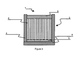
- a device 1 for producing wafers of semiconductor material comprises a crucible 2 having a bottom 3 and side walls 4.
- the device 1 also comprises a mold 5 consisting of spaced apart spacers 6, spaced apart from each other and fixed at their upper end to a movable support 7.
- the Interlayers 6 are for example constituted by flat plates or having a groove or flanges corresponding to the dimensions of the wafers of semiconductor material to be formed.
- a seed 8, made of semiconductor material, is located at the bottom of the crucible 2.
- a charge made of semiconductor material, preferably of microelectronic or photovoltaic quality, is placed in the crucible 2 on the seed 8.
- the material charge semiconductor is for example silicon, germanium or an alloy thereof.
- the seed 8 is made of the same material as the filler.
- the seed 8 is in monocrystalline or polycrystalline form, preferably coarse grain.
- the choice of the crystallinity of the seed 8, monocrystalline or polycrystalline, is a function of the desired crystallinity of the platelets.
- the seed advantageously has on its face in contact with the feed a crystalline orientation along non-dense crystallographic planes of the material of the load. It can be, for example, for the silicon of the plane ⁇ 112>
- the charge of semiconductor material for example silicon
- heating means (not shown), which can be achieved by any suitable technique, while taking care not to melt the seed 8.
- the load is heated laterally for example by inductive turns.
- a liquid silicon phase 9 is then formed above and in contact with the seed 8 and a thermal gradient is created between the seed 8 and the liquid silicon 9.
- the device 1 also comprises, conventionally, a cooling system comprising heat extraction means (not shown), for example a water circulation cooling system, advantageously located under the crucible 2.
- the device 1 further comprises advantageously, means for producing the vacuum in the enclosure of the device (not shown).
- the intermediate elements 6 serve to define the dimensions of the wafers to be molded.
- the intermediate elements 6 of the mold 5 conventionally allow the simultaneous production of a plurality of silicon wafers.
- the silicon wafers thus formed have a thickness generally of between 100 and 500 ⁇ m.
- the wafers may for example be of rectangular or square shape and typically have an area of between 50x50 and 250x250 mm 2 .
- the mold materials 5 are chosen so as not to react chemically with the molten silicon 9, in order to minimize the risk of chemical pollution of the liquid silicon 9.
- the materials used for producing the mold 5, including the intermediate elements 6 are, for example, graphite or other ceramics such as alumina, silicon nitride or silicon carbide. These materials are advantageously coated on their surface with a non-adherent deposit with respect to silicon (not shown).
- This non-stick deposit may for example be a deposit based on silicon nitride powder, the method of production of which is described in particular by Hide ("Mold Shaping Silicon Crystal Growth With a Coating Material by the Spinning Method" Journal of Crystal Growth 79 (1986) 583-589 ) and Saito (A New Directional Solidification Technique for Polycrystalline Solar Grade Silicon® XV IEEE Photovoltaic Specialists Conference, 1981, p.576 ).
- the crucible 2 can be covered by the same non-stick deposit. This type of coating has the advantage of allowing the reuse of the mold 5 for the subsequent manufacture of other silicon wafers.
- the intermediate elements 6 of the mold 5 are advantageously made of a more thermally conductive material than silicon, for example graphite.
- the mold can be filled by the molten silicon 9 by means of a piston.
- the piston is formed by the support 7 of the mold.
- the mold 5 is filled by the molten silicon 9.
- the filling of the mold 5 is complete when it is completely immersed in the liquid silicon 9.
- the mold 5 Prior to its introduction into the liquid silicon 9, the mold 5 is preferably heated to a temperature above the melting temperature of the silicon.
- the mold 5 is first brought into the crucible 2 in direct contact with the seed 8 and the charge of semiconductor material is initially disposed above the intermediate elements 6 of the mold 5.
- the filling of the mold 5 by the molten silicon 9 is then obtained by creating a pressure difference within the device 1, for example, by applying a gas overpressure on the free surface of the molten silicon bath 9 or by suction from the bottom of the intermediate elements 6.
- the thermal gradient existing between the silicon in the liquid phase 9 and the seed 8 is controlled so as to maintain the seed 8 in the solid phase.
- the silicon When the molten silicon 9 fills the mold 5, the silicon is solidified, directed at low speed, typically in a range between 0.01 and 1 cm / min, so as to obtain a good crystalline quality. Directed solidification can be achieved by displacement of the heating and / or controlled cooling system.
- the cooling system allows the heat flow to be unidirectionally discharged in the plane of the silicon wafers, perpendicular to the surface of the seed 8. The use of unidirectional heat extraction makes it possible to minimize the thermomechanical stresses and to obtain a macroscopically plane solidification front leading to a columnar grain structure if the seed 8 is polycrystalline.
- the spacer elements 6 being formed in a more thermally conductive material than silicon, the heat of the wafers is extracted laterally and transmitted to the bottom 3 of the crucible 2 via the intermediate elements 6. If the silicon charge contains very little impurities, the solidification rate remains below the critical rate of morphological destabilization of the solid / liquid front. Under these conditions, the maximum solidification rate is only limited by the heat extraction capacity of the device 1.
- the use of a mold having spacers more thermally conductive than silicon increases the extraction capacity of the device. heat flow with respect to ingot crystallization.
- the use of a seed 8 associated with a mold 6 makes it possible to use a faster rate of solidification than by a process for crystallizing an ingot from a seed.
- a seed 8 having on its upper surface an orientation along non-dense crystallographic planes leads to a lower silicon growth undercooling compared to a seed 8 oriented in dense planes.
- a seed 8 oriented along non-dense crystallographic planes makes it possible to use faster solidification rates, while limiting the supercooling of the liquid to a lower value than that which causes heterogeneous germination ahead of the solidification front and therefore equiaxed growth.
- the reduced size of the space between the intermediate elements 6 constituting the molding element does not allow a good mixing of the liquid silicon 9.
- the segregation of the species including the doping species is limited. It follows that along the (vertical) direction of solidification, for example the distribution of dopants for example phosphorus is more homogeneous than with most other techniques including the crystallization of an ingot. This device is therefore well suited to the production of silicon wafers advantageously doped n-type.
- the silicon wafers are integral with the seed 8. They are then separated from the seed, for example by laser cutting. Thus the seed 8 can be reused for the formation of new silicon wafers. After their release from germ 8, the platelets are directly usable, possibly after removal of a portion of the release coating adhered to their surface.
Landscapes
- Chemical & Material Sciences (AREA)
- Engineering & Computer Science (AREA)
- Crystallography & Structural Chemistry (AREA)
- Materials Engineering (AREA)
- Metallurgy (AREA)
- Organic Chemistry (AREA)
- Silicon Compounds (AREA)
- Crystals, And After-Treatments Of Crystals (AREA)
Applications Claiming Priority (1)
| Application Number | Priority Date | Filing Date | Title |
|---|---|---|---|
| FR0704690A FR2918080B1 (fr) | 2007-06-29 | 2007-06-29 | Dispositif et procede d'elaboration de plaquettes en materiau semi-conducteur par moulage et cristallisation dirigee |
Publications (1)
| Publication Number | Publication Date |
|---|---|
| EP2014802A1 true EP2014802A1 (de) | 2009-01-14 |
Family
ID=39092117
Family Applications (1)
| Application Number | Title | Priority Date | Filing Date |
|---|---|---|---|
| EP08354042A Withdrawn EP2014802A1 (de) | 2007-06-29 | 2008-06-20 | Bearbeitungsverfahren von Scheiben aus Halbleitermaterial durch Formen und gesteuerte Kristallisation |
Country Status (4)
| Country | Link |
|---|---|
| US (1) | US7601618B2 (de) |
| EP (1) | EP2014802A1 (de) |
| JP (1) | JP5425421B2 (de) |
| FR (1) | FR2918080B1 (de) |
Cited By (3)
| Publication number | Priority date | Publication date | Assignee | Title |
|---|---|---|---|---|
| WO2009108358A1 (en) * | 2008-02-29 | 2009-09-03 | Corning Incorporated | Methods of making an unsupported article of pure or doped semiconducting material |
| WO2010132651A1 (en) * | 2009-05-14 | 2010-11-18 | Corning Incorporated | Methods of making an article of semiconducting material on a mold comprising semiconducting material |
| US8540920B2 (en) | 2009-05-14 | 2013-09-24 | Corning Incorporated | Methods of making an article of semiconducting material on a mold comprising particles of a semiconducting material |
Families Citing this family (7)
| Publication number | Priority date | Publication date | Assignee | Title |
|---|---|---|---|---|
| CN102421947B (zh) | 2009-03-09 | 2016-09-28 | 1366科技公司 | 从已熔化材料制造薄半导体本体的方法和装置 |
| US8591795B2 (en) * | 2009-12-04 | 2013-11-26 | Corning Incorporated | Method of exocasting an article of semiconducting material |
| US20120027996A1 (en) * | 2010-07-27 | 2012-02-02 | Glen Bennett Cook | Mold shape to optimize thickness uniformity of silicon film |
| CN101928980B (zh) * | 2010-09-17 | 2012-10-03 | 浙江碧晶科技有限公司 | 一种用于定向凝固法生长硅晶体的引晶导向模 |
| DE102012224196A1 (de) | 2012-12-21 | 2014-06-26 | Siemens Aktiengesellschaft | Ultraschallvorrichtung und Haltegerät zum Reinigen von Bauteiloberflächen |
| US10460955B2 (en) * | 2014-08-25 | 2019-10-29 | The United States Of America As Represented By The Secretary Of The Army | Methodology for annealing group III-nitride semiconductor device structures using novel weighted cover systems |
| WO2026009355A1 (ja) * | 2024-07-03 | 2026-01-08 | ユニオンマテリアル株式会社 | 単結晶ウエハー及びその製造方法 |
Citations (4)
| Publication number | Priority date | Publication date | Assignee | Title |
|---|---|---|---|---|
| EP0115711A1 (de) * | 1983-02-09 | 1984-08-15 | Commissariat à l'Energie Atomique | Verfahren zur Herstellung von Platten aus metallischem oder halbleitendem Material durch Abformen ohne direkte Berührung mit den Wänden der Form |
| GB2139916A (en) * | 1983-05-19 | 1984-11-21 | Mobil Solar Energy Corp | EFG Apparatus |
| JP2001163698A (ja) * | 1999-12-06 | 2001-06-19 | Hitachi Cable Ltd | 液相エピタキシャル成長方法 |
| EP1329538A2 (de) * | 1995-09-29 | 2003-07-23 | Union Material Inc. | Verfahren zur Herstellung geformter Kristalle durch Aufwärtsspritzen einer Flüssigkeit unter Druck |
Family Cites Families (5)
| Publication number | Priority date | Publication date | Assignee | Title |
|---|---|---|---|---|
| JP2947529B2 (ja) | 1991-03-19 | 1999-09-13 | ユニオンマテリアル株式会社 | 整形結晶の製造方法及び製造装置 |
| JP3151759B2 (ja) * | 1994-12-22 | 2001-04-03 | モリックス株式会社 | 熱電半導体針状結晶及び熱電半導体素子の製造方法 |
| US6774009B1 (en) * | 2001-03-27 | 2004-08-10 | Academy Corporation | Silicon target assembly |
| KR101470814B1 (ko) * | 2006-01-20 | 2014-12-09 | 에이엠지 아이디얼캐스트 솔라 코포레이션 | 광전 변환 소자용 단결정 캐스트 실리콘 및 단결정 캐스트 실리콘 바디들을 제조하는 방법 및 장치 |
| US7547360B2 (en) * | 2006-09-27 | 2009-06-16 | Ii-Vi Incorporated | Reduction of carbon inclusions in sublimation grown SiC single crystals |
-
2007
- 2007-06-29 FR FR0704690A patent/FR2918080B1/fr active Active
-
2008
- 2008-06-20 EP EP08354042A patent/EP2014802A1/de not_active Withdrawn
- 2008-06-24 US US12/213,751 patent/US7601618B2/en not_active Expired - Fee Related
- 2008-06-30 JP JP2008170776A patent/JP5425421B2/ja not_active Expired - Fee Related
Patent Citations (4)
| Publication number | Priority date | Publication date | Assignee | Title |
|---|---|---|---|---|
| EP0115711A1 (de) * | 1983-02-09 | 1984-08-15 | Commissariat à l'Energie Atomique | Verfahren zur Herstellung von Platten aus metallischem oder halbleitendem Material durch Abformen ohne direkte Berührung mit den Wänden der Form |
| GB2139916A (en) * | 1983-05-19 | 1984-11-21 | Mobil Solar Energy Corp | EFG Apparatus |
| EP1329538A2 (de) * | 1995-09-29 | 2003-07-23 | Union Material Inc. | Verfahren zur Herstellung geformter Kristalle durch Aufwärtsspritzen einer Flüssigkeit unter Druck |
| JP2001163698A (ja) * | 1999-12-06 | 2001-06-19 | Hitachi Cable Ltd | 液相エピタキシャル成長方法 |
Cited By (6)
| Publication number | Priority date | Publication date | Assignee | Title |
|---|---|---|---|---|
| WO2009108358A1 (en) * | 2008-02-29 | 2009-09-03 | Corning Incorporated | Methods of making an unsupported article of pure or doped semiconducting material |
| US8617447B2 (en) | 2008-02-29 | 2013-12-31 | Corning Incorporated | Methods of making an unsupported article of pure or doped semiconducting material |
| WO2010132651A1 (en) * | 2009-05-14 | 2010-11-18 | Corning Incorporated | Methods of making an article of semiconducting material on a mold comprising semiconducting material |
| CN102597335A (zh) * | 2009-05-14 | 2012-07-18 | 康宁股份有限公司 | 在包括半导体材料的模具上制造半导体材料制品的方法 |
| US8398768B2 (en) | 2009-05-14 | 2013-03-19 | Corning Incorporated | Methods of making an article of semiconducting material on a mold comprising semiconducting material |
| US8540920B2 (en) | 2009-05-14 | 2013-09-24 | Corning Incorporated | Methods of making an article of semiconducting material on a mold comprising particles of a semiconducting material |
Also Published As
| Publication number | Publication date |
|---|---|
| FR2918080B1 (fr) | 2010-12-17 |
| US7601618B2 (en) | 2009-10-13 |
| FR2918080A1 (fr) | 2009-01-02 |
| US20090004835A1 (en) | 2009-01-01 |
| JP5425421B2 (ja) | 2014-02-26 |
| JP2009013055A (ja) | 2009-01-22 |
Similar Documents
| Publication | Publication Date | Title |
|---|---|---|
| FR2918080A1 (fr) | Dispositif et procede d'elaboration de plaquettes en materiau semi-conducteur par moulage et cristallisation dirigee | |
| EP2089319B1 (de) | Verfahren zur reinigung von metallurgischem silicium durch gerichtete erstarrung | |
| EP2014803B1 (de) | Vorrichtung zur Herstellung eines Blocks aus kristallinem Material mit Modulation der Wärmeleitfähigkeit | |
| CN102127805A (zh) | 连续浇铸单晶硅带的设备和方法 | |
| KR20100123745A (ko) | 순수 또는 도핑된 반도체 물질의 비지지 제품을 제조하는 방법 | |
| JP7145763B2 (ja) | パターン形成された突起構造層を有するシリコンインゴット成長用のるつぼ | |
| EP3198061B1 (de) | Schmelztiegel zur gerichteten erstarrung von multi- kristallinem oder quasi-einkristallinem silizium auf keim(en) | |
| US20100291380A1 (en) | Methods of making an article of semiconducting material on a mold comprising particles of a semiconducting material | |
| JP4060106B2 (ja) | 一方向凝固シリコンインゴット及びこの製造方法並びにシリコン板及び太陽電池用基板及びスパッタリング用ターゲット素材 | |
| JP2007019209A (ja) | 太陽電池用多結晶シリコンおよびその製造方法 | |
| JP6401051B2 (ja) | 多結晶シリコンインゴットの製造方法 | |
| JP4011335B2 (ja) | 固相シートの製造方法 | |
| WO2007048904A1 (fr) | Dispositif de fabrication d'un ruban de silicium ou autres materiaux cristallins et procede de fabrication | |
| JP4497943B2 (ja) | シリコン鋳造用鋳型とそれを用いたシリコン鋳造装置 | |
| JP2008239438A (ja) | 球状結晶の製造方法及び製造装置 | |
| KR20140006940A (ko) | 거대 입자 다결정 실리콘막을 형성하기 위한 방법 및 제품 | |
| JP2004322195A (ja) | 一方向凝固シリコンインゴット及びこの製造方法並びにシリコン板及び太陽電池用基板 | |
| KR20140033411A (ko) | 복합 활성 몰드 및 반도체 물질의 제품을 제조하기 위한 방법 | |
| EP0115711B1 (de) | Verfahren zur Herstellung von Platten aus metallischem oder halbleitendem Material durch Abformen ohne direkte Berührung mit den Wänden der Form | |
| TWI642819B (zh) | 製造半導體薄片之方法及執行該方法之製造設備 | |
| JP6487675B2 (ja) | 多結晶シリコンインゴット製造方法、多結晶シリコンインゴットの用途の製造方法及び多結晶シリコンインゴット | |
| FR3105267A1 (fr) | Procédé de solidification par tirage au moyen d’une filière flottante | |
| WO2013105019A1 (fr) | Procede de preparation de silicium a l'etat solide |
Legal Events
| Date | Code | Title | Description |
|---|---|---|---|
| PUAI | Public reference made under article 153(3) epc to a published international application that has entered the european phase |
Free format text: ORIGINAL CODE: 0009012 |
|
| AK | Designated contracting states |
Kind code of ref document: A1 Designated state(s): AT BE BG CH CY CZ DE DK EE ES FI FR GB GR HR HU IE IS IT LI LT LU LV MC MT NL NO PL PT RO SE SI SK TR |
|
| AX | Request for extension of the european patent |
Extension state: AL BA MK RS |
|
| 17P | Request for examination filed |
Effective date: 20090627 |
|
| AKX | Designation fees paid |
Designated state(s): AT BE BG CH CY CZ DE DK EE ES FI FR GB GR HR HU IE IS IT LI LT LU LV MC MT NL NO PL PT RO SE SI SK TR |
|
| 17Q | First examination report despatched |
Effective date: 20090922 |
|
| RAP1 | Party data changed (applicant data changed or rights of an application transferred) |
Owner name: COMMISSARIAT A L'ENERGIE ATOMIQUE ET AUX ENERGIES |
|
| 17Q | First examination report despatched |
Effective date: 20110811 |
|
| STAA | Information on the status of an ep patent application or granted ep patent |
Free format text: STATUS: EXAMINATION IS IN PROGRESS |
|
| STAA | Information on the status of an ep patent application or granted ep patent |
Free format text: STATUS: THE APPLICATION IS DEEMED TO BE WITHDRAWN |
|
| 18D | Application deemed to be withdrawn |
Effective date: 20200103 |