EP2015087A1 - Dispositif de test de composants électroniques, en particulier IC, doté d'une carte d'étanchéité installée à l'intérieur d'une chambre de test de la pression - Google Patents
Dispositif de test de composants électroniques, en particulier IC, doté d'une carte d'étanchéité installée à l'intérieur d'une chambre de test de la pression Download PDFInfo
- Publication number
- EP2015087A1 EP2015087A1 EP08011535A EP08011535A EP2015087A1 EP 2015087 A1 EP2015087 A1 EP 2015087A1 EP 08011535 A EP08011535 A EP 08011535A EP 08011535 A EP08011535 A EP 08011535A EP 2015087 A1 EP2015087 A1 EP 2015087A1
- Authority
- EP
- European Patent Office
- Prior art keywords
- contact
- contact element
- pressure chamber
- element sections
- components
- Prior art date
- Legal status (The legal status is an assumption and is not a legal conclusion. Google has not performed a legal analysis and makes no representation as to the accuracy of the status listed.)
- Granted
Links
- 238000012360 testing method Methods 0.000 title claims abstract description 53
- 238000007789 sealing Methods 0.000 title claims abstract description 9
- 230000000149 penetrating effect Effects 0.000 claims description 2
- 238000006243 chemical reaction Methods 0.000 description 4
- 238000000034 method Methods 0.000 description 3
- 125000006850 spacer group Chemical group 0.000 description 3
- 238000005259 measurement Methods 0.000 description 2
- 230000006978 adaptation Effects 0.000 description 1
- 239000002131 composite material Substances 0.000 description 1
- 150000001875 compounds Chemical class 0.000 description 1
- 238000001514 detection method Methods 0.000 description 1
- 238000006073 displacement reaction Methods 0.000 description 1
- 238000004519 manufacturing process Methods 0.000 description 1
- 239000011159 matrix material Substances 0.000 description 1
Images


Classifications
-
- G—PHYSICS
- G01—MEASURING; TESTING
- G01R—MEASURING ELECTRIC VARIABLES; MEASURING MAGNETIC VARIABLES
- G01R31/00—Arrangements for testing electric properties; Arrangements for locating electric faults; Arrangements for electrical testing characterised by what is being tested not provided for elsewhere
- G01R31/28—Testing of electronic circuits, e.g. by signal tracer
- G01R31/2851—Testing of integrated circuits [IC]
- G01R31/2855—Environmental, reliability or burn-in testing
- G01R31/2872—Environmental, reliability or burn-in testing related to electrical or environmental aspects, e.g. temperature, humidity, vibration, nuclear radiation
- G01R31/2881—Environmental, reliability or burn-in testing related to electrical or environmental aspects, e.g. temperature, humidity, vibration, nuclear radiation related to environmental aspects other than temperature, e.g. humidity or vibrations
-
- G—PHYSICS
- G01—MEASURING; TESTING
- G01R—MEASURING ELECTRIC VARIABLES; MEASURING MAGNETIC VARIABLES
- G01R31/00—Arrangements for testing electric properties; Arrangements for locating electric faults; Arrangements for electrical testing characterised by what is being tested not provided for elsewhere
- G01R31/28—Testing of electronic circuits, e.g. by signal tracer
- G01R31/2851—Testing of integrated circuits [IC]
- G01R31/2855—Environmental, reliability or burn-in testing
- G01R31/286—External aspects, e.g. related to chambers, contacting devices or handlers
- G01R31/2862—Chambers or ovens; Tanks
Definitions
- the invention relates to a device for testing electronic components, in particular ICs under certain pressure conditions, according to the preamble of claim 1.
- Electronic components such as MEMS (Micro-Electro-Mechanical System) used for pressure detection are usually subjected to pressure tests after their production in order to check their proper functioning or to compensate for their characteristic curve at different temperatures, ie to calibrate. For this it is sometimes necessary to determine several hundred parameters.
- the pressure tests take place in pressure test chambers, which consist of two separable pressure chamber halves.
- the components to be tested are placed in one of the pressure chamber halves, whereupon these pressure chamber half then against the other pressure chamber half is driven until it is in close contact with this other half of the pressure chamber. In this process, contacts of the components are connected with contact elements projecting into the cavity of the pressure test chamber and leading to an electronic test device.
- the desired test pressure within the cavity of the pressure test chamber can be built up as quickly as possible and maintained constant during the test. It is therefore necessary reliably seal the cavity to the outside.
- the seal must often be able to withstand high test pressures of, for example, 20 bar or more.
- the pressure test chambers should be constructed so that they can be converted in the simplest possible way for different components.
- the invention has for its object to provide a device for testing electronic components, in particular IC's, under certain pressure conditions, which is as simple as possible and adaptable to different components in a simple and cost-effective manner and maintains the desired pressure conditions in a reliable manner.
- each contact element is subdivided into a first contact element section penetrating the pressure chamber half and a second contact element section spaced from the first contact element section, which is arranged inside the cavity.
- an air-permeable Abdichtboard is arranged, which extends transversely across the contact elements and the edge sealed to the associated pressure chamber half, wherein the first contact element sections are arranged on one side of the Abdichtboards and the first contact element sections associated second contact element sections on the opposite side of the Abdichtboards , Furthermore, the first contact element sections electrically connected to the opposite second contact element portions via conductive portions of the Abdichtboards.
- the device according to the invention it is thus not necessary to seal the first contact element sections, which penetrate the pressure chamber and extend outward from the cavity, individually. Rather, all first contact element sections are sealed together by the Abdichtboard. On the opposite side of the Abdichtboards then the second contact element sections are fixed, which - separated by the Abdichtboard - are already in that region of the cavity in which the desired test pressure is built up.
- a component-specific DUT board is provided, which is arranged within the cavity between the second contact element sections and the third contact element sections spaced from the second contact element sections, with which the contacts of the components can be brought into contact.
- a darieri design allows a particularly simple conversion of the device with different components and strip geometries. The number of parts to be changed during conversion can be greatly reduced. It is particularly advantageous that the Abdichtboard can remain identical even with different components and strip geometries and - since the component-specific adaptation already takes place through the arranged inside the cavity DUT board - and the outside of the pressure test chamber to the contact elements subsequent facilities, such as an interface board and / or A DIB (Data Input Bus Board) board can remain the same. As a result, the conversion costs and the conversion time can be reduced.
- DIB Data Input Bus Board
- a component-specific DUT board is provided, which is arranged outside the pressure test chamber and in contact with the first contact element sections, while the second contact element sections are adapted to the contacts of the components to be tested and face these contacts, the contacts of the components can be brought into contact with the second contact element sections.
- At least the first contact element sections consist of spring pins which are resilient in their longitudinal direction (pogo pins). It is advantageous if the second contact element sections and optionally also the third contact element sections consist of such resilient contact pins. Alternatively, however, it is also conceivable that those contact element portions with which the components are brought into contact, are designed differently, for example, have the form of curved contact springs.
- FIG. 1 a pressure test chamber with a first, lower pressure chamber half 1 and a second, upper pressure chamber half 2 can be seen.
- the upper pressure chamber half 2 is arranged stationary, while the lower pressure chamber half 1 by means of a lifting device, not shown in the vertical direction, ie in the z-direction, can be raised or lowered.
- FIG. 1 a two swing jaws 3 comprehensive locking mechanism can be seen.
- the swivel jaws 3 are about pivot axes 4 between a in FIG. 1 shown opening position and one in the Figures 2 and 3 pivoted lock position shown.
- the two pivot axes 4 are parallel to each other and can either - as in FIG. 1 shown - be mounted on the upper half of the pressure chamber 2 or alternatively also above the pressure chamber half. 2
- the two pressure chamber halves 1, 2 have at least substantially a rectangular shape in plan view.
- the lower pressure chamber half 1 has a recess 5, in which a plurality of juxtaposed components 18 (FIG. FIGS. 2 to 4 ) can be used when the lower pressure chamber half 1 is at a sufficient distance from the upper pressure chamber half 3.
- the components 18 are adjacent to each other in the form of a composite, which is formed as a rectangular strip 6.
- Each strip 6 can have a plurality of components 18 both in the longitudinal and in the transverse direction, which are arranged in matrix form in the xy plane.
- the strip 6 can be placed on a strip tray 7 (FIG. FIGS. 1 and 3 ) and placed together with the strip tray 7 in the recess 5 of the lower pressure chamber half 1. It is also possible to insert the strip 6 without the strip tray 7 in the recess 5, if the lower pressure chamber half 1 itself has a corresponding support means for the strip 6.
- the upper pressure chamber half 2 has a recess 8 which is opposite to the recess 5 of the lower pressure chamber half 1 and together with this forms a closed cavity when the lower pressure chamber half 1 is moved up to the upper pressure chamber half 2.
- the pressure chamber halves 1, 2 have mutually facing surfaces 9, 10, which are parallel to each other and flat.
- a seal 12 is embedded in the form of an O-ring. The seal 12 is down over the Surface 10 before, so that the surface 9 of the lower pressure chamber half 1 can be pressed against the seal 12, whereby the cavity is closed pressure-tight with compressed pressure chamber halves 1, 2 together.
- contact elements 13 project into the cavity, which can be brought into contact with corresponding contacts of the components 18 placed in the recess 5 when the two pressure chamber halves 1, 2 are moved together.
- the contact elements 13 extend, as described below with reference to FIGS. 2 to 4 will be explained in more detail, through the upper half of the pressure chamber 2 through the outside of the pressure test chamber and are connected to an electronic test device, not shown, conveniently via a test head.
- each pivoting jaw 3 has at least one lifting device, not shown, which comprises a pivoting jaw 3 arranged in the pneumatic cylinder, which acts on a plunger 17 via a lever mechanism.
- the plunger 17 is mounted longitudinally displaceable in the support portion 15 and can be moved from a substantially retracted position, the FIG. 1 is shown, are extended by means of the piston upwards over the support portion 15, so that he closed bottom jaws 3, the lower half of the pressure chamber 1 firmly against the upper pressure chamber half 2 or against the seal 12 presses, so that the cavity is sealed.
- the swivel jaws 3 may have a mechanical locking device, not shown, can be inserted with the spacer plates in the space between the support portions 15 and the edge portions 16 of the lower pressure chamber half 1, after the plunger 17, the lower pressure chamber half 1 against the seal 12 of the upper pressure chamber half. 2 pressed. In this way, the tight contact of the lower pressure chamber half 1 can be maintained at the upper pressure chamber half 2 in a mechanical manner, so that the lifting devices can be relieved.
- the lower pressure chamber half 1 is raised by means of the lifting device, not shown, in the z-direction to the immediate vicinity of the upper pressure chamber half, the lower pressure chamber half 1 is positioned in a precise test position relative to the upper pressure chamber half 2.
- the two pivoting jaws 3 are pivoted inwardly, wherein the support portions 15, the edge portions 16 of the lower pressure chamber half 1 engage under.
- the plunger 17 are extended upward, so that the lower pressure chamber half 1 is pressed against the seal of the upper pressure chamber half 2, and this seal 12 deforms correspondingly elastic.
- the spacer plates are retracted by means of the mechanical locking device into the intermediate space between the support sections 15 of the swivel jaws 3 and the lower pressure chamber half 1.
- the plunger 17 can now be moved back, the dense system of the lower pressure chamber half 1 is maintained at the seal 12. In this position, the contacts of the components 18 are contacted with the contact elements 13 of the upper pressure chamber half 2.
- the desired test pressure is built up in the cavity. If this test pressure is reached, the electronic measurement of the components 18 is performed.
- the pressure in the cavity is reduced.
- the plungers 17 are extended for a short time in order to be able to pull back the spacer plates. Then the plunger 17 are retracted back into the support portions 15.
- the swivel jaws 3 can now return to the in FIG. 1 shown opened position, whereupon the lower pressure chamber half 1 is moved away from the upper half of the pressure chamber, so that the tested components 18, optionally with the striptape 7, from the lower pressure chamber half 1 can be removed.
- the pressure test chamber can thus be loaded again with new components 18.
- the lower pressure chamber half 1 can be displaceable relative to the upper pressure chamber half 2 in the x- and / or y-direction and / or about the z-axis, so that the number of contact elements 13 is lower than that of the contacts of the components 18 inserted into the cavity can be. In this case, at first only a part of the inserted components 18 is contacted and tested, then the lower pressure chamber half 1 is displaced and / or rotated and subsequently a further part of the inserted components 18 is contacted and tested. This process is repeated until all inserted components 18 have been contacted and tested. Only then is the pressure chamber half 1 lowered so far that the tested components 18 are removed and new components 18 can be inserted. However, this type of stepwise testing with lateral displacement and / or rotation of the lower pressure chamber half 1 is merely optional in the context of the present invention.
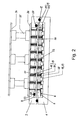
- the contact element sections 19, 20 consist in the illustrated embodiment in each case of resilient pins (Pogo pins), wherein a plurality of adjacent pins in the form of so-called Pogo stacks 21, 22 may be bundled.
- the first contact element portions 19 and Pogo stacks 21 penetrate the upper wall 23 of the upper pressure chamber half 2.
- the outer ends of the first contact element portions 19 are associated with contacts of a DUT board 24 (Device Under Test Board) in electrical contact, which is located above the upper pressure chamber half 2 and thus outside of the pressure test chamber.
- the DUT board 24 is a component-specific, exchangeable board.
- the DUT board 24 is connected via electrical connection elements 25 to a DIB board (Data Input Bus Board), via which an electrical connection to the (not shown) electronic test device is provided.
- DIB board Data Input Bus Board
- the inner ends of the first contact element portions 19 that extend inwardly slightly beyond the underside of the upper wall 23 are in contact with associated contacts on the top of a sealing board 26.
- the Abdichtboard 26 is formed as an airtight plate or board, which extends transversely to the longitudinal extent of the contact elements 13 over all contact elements 13 and the first contact element portions 19 from the second contact element sections 20 spatially separated.
- the Abdichtboard 26 is attached to the wall 23 of the upper pressure chamber half 2 and sealed in its edge region by means of a circumferential seal 27 against the wall 23 airtight.
- the Abdichtboard 26 thus prevents air or other gas from the Kavticians Symposium in which the test pressure is built (by means not shown lines) through the openings in the wall 23 in which the first contact element portions 19 or Pogo stacks 21 are arranged can go outside (or inside).
- the Abdichtboard 26 has on its underside electrical contacts which correspond to the contacts on its upper side and are electrically connected thereto. At These lower-side contacts are the upper ends of the second contact element portions 20, so that they are electrically connected to the respective associated first contact element portions 19.
- the second contact element portions 20 or Pogo stacks 22 are in contact sockets, which are attached from below to Abdichtboard 26.
- the lower ends of the second contact element sections 20 are arranged corresponding to the contacts of the components 18 to be tested, so that the component contacts can be contacted with the second contact element sections 20 when the lower pressure chamber half 1 is pressed into tight contact with the upper pressure chamber half 2.
- the seal 12 prevents air from passing between the pressure chamber halves 1, 2 out of the cavity to the outside or vice versa from the outside into the cavity, as shown by FIG. 1 has been described.
- the strip 6 is placed on a plurality of support elements 28 (lead backers) which are located at the bottom of the recess 5 and support the strip 6 in the area of the component contacts.
- the component body 29 is arranged between support elements 28.
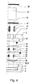
- This second embodiment differs from the first embodiment described above essentially in that the DUT board 24 is not disposed outside, but within the cavity of the pressure test chamber and between the Abdichtboard 26th and the devices 18 to be tested.
- the two pressure chamber halves 1, 2, their mutual sealing by means of the seal 12, the first contact element portions 19 and Pogo stacks 21 and their sealing means of the Abdichtboards 26 and the seal 27 are the same or quite similar to the first embodiment formed and arranged so that in this regard reference is made to the first embodiment.
- the DUT board 24 is arranged parallel to the sealing board 26, ie horizontally in the present embodiment, between the lower ends of the second contact element sections 20 and associated third contact element sections 30.
- the third contact element sections 30 in turn consist of resilient contact pins (Pogo pins), which are arranged according to the contacts of the components 18 to be contacted, so that the component contacts with the third contact element sections 30 can be contacted when the lower pressure chamber half 1 in tight contact with the upper Pressure chamber half 2 is pressed.
- the third contact element sections 30 may in turn be bundled in the form of pogo stacks 31 and are fixed by means of contact sockets on the underside of the DUT board 24.
- the replaceable, component-specific DUT board 24 is used in this embodiment to through-contact the third contact element sections 30 to the second contact element sections 20 and thereby the component-specific arranged and formed third contact element sections 30 with the associated second contact element sections 20 to be contacted, which need not be specific to the building and / or trained.
- This second embodiment thus has the advantage that when changing the type of components to be tested only the DUT board 24 and the third contact element sections 30 must be replaced on the side of the upper half of the pressure chamber 2, while the components arranged above the DUT boards 24 can be used universally are, that are suitable for different types of components.
- the strip 6 is located in the region of the component contacts on support elements 28 (lead backers), which are arranged on an insertable into the recess 5 Striptablett 7.
- the upper ends of the first contact element sections 19 are in contact with a universal interface board 32, which is arranged above the upper pressure chamber half 2 and thus outside the pressure test chamber.
- This interface board 32 is again in contact via a universal punch-through board 33 (through board) with a DIB board 34 (Data Input Bus Board).
- DIB board 34 Data Input Bus Board
- the interface board, puncture board 33 and DIB board 34 are thus equally suitable for testing different types of components.
Landscapes
- Engineering & Computer Science (AREA)
- Environmental & Geological Engineering (AREA)
- Health & Medical Sciences (AREA)
- Toxicology (AREA)
- Computer Hardware Design (AREA)
- Microelectronics & Electronic Packaging (AREA)
- General Engineering & Computer Science (AREA)
- Physics & Mathematics (AREA)
- General Physics & Mathematics (AREA)
- Testing Of Individual Semiconductor Devices (AREA)
Applications Claiming Priority (1)
| Application Number | Priority Date | Filing Date | Title |
|---|---|---|---|
| DE102007032557A DE102007032557B4 (de) | 2007-07-12 | 2007-07-12 | Vorrichtung zum Testen von elektronischen Bauelementen, insbesondere IC's, mit innerhalb einer Drucktestkammer angeordnetem Abdichtboard |
Publications (2)
| Publication Number | Publication Date |
|---|---|
| EP2015087A1 true EP2015087A1 (fr) | 2009-01-14 |
| EP2015087B1 EP2015087B1 (fr) | 2011-12-21 |
Family
ID=39709098
Family Applications (1)
| Application Number | Title | Priority Date | Filing Date |
|---|---|---|---|
| EP08011535A Ceased EP2015087B1 (fr) | 2007-07-12 | 2008-06-25 | Dispositif de test de composants électroniques, en particulier IC, doté d'une carte d'étanchéité installée à l'intérieur d'une chambre de test de la pression |
Country Status (4)
| Country | Link |
|---|---|
| US (1) | US7633304B2 (fr) |
| EP (1) | EP2015087B1 (fr) |
| DE (1) | DE102007032557B4 (fr) |
| MY (1) | MY147709A (fr) |
Cited By (2)
| Publication number | Priority date | Publication date | Assignee | Title |
|---|---|---|---|---|
| EP2672283A1 (fr) * | 2012-06-05 | 2013-12-11 | Multitest elektronische Systeme GmbH | Dispositif de test, système de test, procédé et support pour tester des composants électroniques dans des conditions de pression variable |
| CN113433410A (zh) * | 2021-07-02 | 2021-09-24 | 国网山东省电力公司菏泽供电公司 | 一种多功能电力元器件检测装置 |
Families Citing this family (10)
| Publication number | Priority date | Publication date | Assignee | Title |
|---|---|---|---|---|
| US8564304B2 (en) | 2010-04-23 | 2013-10-22 | AFA Micro Co. | Integrated circuit device test apparatus |
| US9751757B2 (en) * | 2013-03-04 | 2017-09-05 | Kionix, Inc. | Single motor dynamic calibration unit |
| KR102243278B1 (ko) * | 2014-09-18 | 2021-04-23 | 삼성전자주식회사 | 핸들러 및 그의 관리 방법 |
| US10330202B2 (en) * | 2015-03-18 | 2019-06-25 | Nok Corporation | Sealing device |
| TWI640056B (zh) * | 2017-12-28 | 2018-11-01 | 京元電子股份有限公司 | 半導體元件測試載盤及其測試裝置與設備 |
| CN108444827A (zh) * | 2018-04-28 | 2018-08-24 | 无锡盛赛传感科技有限公司 | 一种传感器陶瓷膜片耐压测试装置 |
| CN111190087B (zh) * | 2018-11-15 | 2022-03-15 | 京元电子股份有限公司 | 具浮动容置座的半导体元件测试载盘及其测试设备 |
| DE102019004446B4 (de) * | 2019-06-24 | 2025-08-28 | Yamaichi Electronics Deutschland Gmbh | Testvorrichtung zum Testen elektrischer Bauteile, Verfahren zum Testen elektrischer Bauteile mittels der Testvorrichtung und Verwendung der Testvorrichtung |
| TWI718815B (zh) * | 2019-12-18 | 2021-02-11 | 四方自動化機械股份有限公司 | 多晶片多功能測試系統 |
| AT526936B1 (de) * | 2023-04-18 | 2024-09-15 | Rainer Gaggl Dipl Ing Dr | Vorrichtung zum elektrischen Prüfen von Halbleiterbauelementen |
Citations (7)
| Publication number | Priority date | Publication date | Assignee | Title |
|---|---|---|---|---|
| GB2285348A (en) * | 1993-12-28 | 1995-07-05 | Yamaichi Electronics Co Ltd | Connector with contacts pressed together by gas pressure difference |
| US6072325A (en) * | 1993-07-20 | 2000-06-06 | Tokyo Electron Kabushiki Kaisha | Probe device |
| EP1011134A1 (fr) * | 1998-12-18 | 2000-06-21 | Fujitsu Limited | Contacteur pour dispositifs semi-conducteurs, dispositif de test utilisant un tel contacteur, méthode de test utilisant un tel contacteur et méthode de nettoyage d'un tel contacteur |
| WO2001013130A1 (fr) * | 1999-08-17 | 2001-02-22 | Formfactor, Inc. | Contacteur electrique, plus particulierement contacteur au niveau de la plaquette, utilisant la pression par fluide |
| EP1186903A2 (fr) | 2000-08-28 | 2002-03-13 | Nec Corporation | Dispositif et méthode d'inspection de plaquettes |
| US6812718B1 (en) * | 1999-05-27 | 2004-11-02 | Nanonexus, Inc. | Massively parallel interface for electronic circuits |
| EP1596429A1 (fr) * | 2003-02-18 | 2005-11-16 | JSR Corporation | Connecteur conducteur anisotrope, element de sonde et dispositif et procede d'inspection de tranche |
Family Cites Families (6)
| Publication number | Priority date | Publication date | Assignee | Title |
|---|---|---|---|---|
| US3016489A (en) * | 1959-07-17 | 1962-01-09 | Drexel Dynamics Corp | Test jig for contacting circuit card positions |
| US4777716A (en) * | 1986-08-25 | 1988-10-18 | Motorola Inc. | Method for low pressure testing of a solid state pressure sensor |
| US5336992A (en) * | 1992-06-03 | 1994-08-09 | Trw Inc. | On-wafer integrated circuit electrical testing |
| US5479109A (en) * | 1992-06-03 | 1995-12-26 | Trw Inc. | Testing device for integrated circuits on wafer |
| DE19654404A1 (de) * | 1996-12-24 | 1998-06-25 | Hewlett Packard Co | Adaptationsvorrichtung zum elektrischen Test von Leiterplatten |
| US7368930B2 (en) * | 2006-08-04 | 2008-05-06 | Formfactor, Inc. | Adjustment mechanism |
-
2007
- 2007-07-12 DE DE102007032557A patent/DE102007032557B4/de not_active Expired - Fee Related
-
2008
- 2008-06-25 EP EP08011535A patent/EP2015087B1/fr not_active Ceased
- 2008-07-04 MY MYPI20082478A patent/MY147709A/en unknown
- 2008-07-09 US US12/169,899 patent/US7633304B2/en not_active Expired - Fee Related
Patent Citations (7)
| Publication number | Priority date | Publication date | Assignee | Title |
|---|---|---|---|---|
| US6072325A (en) * | 1993-07-20 | 2000-06-06 | Tokyo Electron Kabushiki Kaisha | Probe device |
| GB2285348A (en) * | 1993-12-28 | 1995-07-05 | Yamaichi Electronics Co Ltd | Connector with contacts pressed together by gas pressure difference |
| EP1011134A1 (fr) * | 1998-12-18 | 2000-06-21 | Fujitsu Limited | Contacteur pour dispositifs semi-conducteurs, dispositif de test utilisant un tel contacteur, méthode de test utilisant un tel contacteur et méthode de nettoyage d'un tel contacteur |
| US6812718B1 (en) * | 1999-05-27 | 2004-11-02 | Nanonexus, Inc. | Massively parallel interface for electronic circuits |
| WO2001013130A1 (fr) * | 1999-08-17 | 2001-02-22 | Formfactor, Inc. | Contacteur electrique, plus particulierement contacteur au niveau de la plaquette, utilisant la pression par fluide |
| EP1186903A2 (fr) | 2000-08-28 | 2002-03-13 | Nec Corporation | Dispositif et méthode d'inspection de plaquettes |
| EP1596429A1 (fr) * | 2003-02-18 | 2005-11-16 | JSR Corporation | Connecteur conducteur anisotrope, element de sonde et dispositif et procede d'inspection de tranche |
Cited By (2)
| Publication number | Priority date | Publication date | Assignee | Title |
|---|---|---|---|---|
| EP2672283A1 (fr) * | 2012-06-05 | 2013-12-11 | Multitest elektronische Systeme GmbH | Dispositif de test, système de test, procédé et support pour tester des composants électroniques dans des conditions de pression variable |
| CN113433410A (zh) * | 2021-07-02 | 2021-09-24 | 国网山东省电力公司菏泽供电公司 | 一种多功能电力元器件检测装置 |
Also Published As
| Publication number | Publication date |
|---|---|
| MY147709A (en) | 2013-01-15 |
| EP2015087B1 (fr) | 2011-12-21 |
| US7633304B2 (en) | 2009-12-15 |
| DE102007032557B4 (de) | 2010-09-16 |
| DE102007032557A1 (de) | 2009-01-15 |
| US20090015277A1 (en) | 2009-01-15 |
Similar Documents
| Publication | Publication Date | Title |
|---|---|---|
| EP2015087B1 (fr) | Dispositif de test de composants électroniques, en particulier IC, doté d'une carte d'étanchéité installée à l'intérieur d'une chambre de test de la pression | |
| DE102004057775B4 (de) | Handhabungsvorrichtung zum Zuführen von elektronischen Bauelementen, insbesondere IC's, zu einer Testvorrichtung | |
| DE102012112271A1 (de) | Zusammenführvorrichtung | |
| DE102015119181B4 (de) | Prüfvorrichtung und Verwendung einer solchen | |
| EP2918351A1 (fr) | Dispositif de vérification de composants électroniques | |
| EP0204291B1 (fr) | Dispositif à tester et trier des composants électroniques, en particulier des puces intégrées | |
| EP1902325B1 (fr) | Dispositif de test pour tester des composants électroniques | |
| DE102004057776A1 (de) | Lagekorrektureinrichtung zur Korrektur der Position eines Bauelementehalters für elektronische Bauelemente | |
| DE19901922A1 (de) | Vorrichtung zum Be-/Entladen eines modularen IC's in eine bzw. aus einer Buchse einer Handhabe für modulare IC's | |
| DE2905175C2 (de) | Adaptiervorrichtung für das Verbinden von zu prüfenden Elektronikbaugruppen mit Prüfgeräten | |
| EP2142935B1 (fr) | Mécanisme de fermeture pour chambres d'essai de pression pour tester des composants électroniques, en particulier des circuits intégrés | |
| DE102012209353B4 (de) | Prüfvorrichtung zum Testen einer Flachbaugruppe | |
| DE102020131098A1 (de) | Vorrichtung zum Verschließen von pharmazeutischen Behältnissen | |
| EP3847466A1 (fr) | Procédé de positionnement d'un substrat d'essai, de sondes et d'une unité d'inspection l'un par rapport à l'autre, et appareil de test pour la mise en ?uvre de ce procédé | |
| EP3715863B1 (fr) | Dispositif destiné aux essais des composants électriques, utilisation du dispositif d'essai pour faire des essais sur un composant électrique et procédé d'essai des composants électriques au moyen du dispositif d'essai | |
| DE2625738C2 (de) | Automatische Einrichtung zum Bestücken von Leiterplatten | |
| DE2918030A1 (de) | Vorrichtung zum pruefen von formationen aus zigaretten | |
| DE3248796C2 (de) | Pneumatische Kontaktiereinrichtung zur automatischen Prüfung von Flachbaugruppen | |
| CH633403A5 (de) | Vorrichtung zum pruefen und bearbeiten elektromechanischer und elektronischer bauteile. | |
| DE4419700A1 (de) | Vorrichtung zur Aufnahme von Werkstücken für Bearbeitungsvorgänge, insbesondere zum Nähen | |
| DE202020103655U1 (de) | Prüfadapter zum Prüfen einer Platine | |
| DE102016102836A1 (de) | Vorrichtung zum Ausrichten von zwei Testeinheiten | |
| DE2323174A1 (de) | Vorrichtung fuer den transport von gefertigten werkstuecken und fuer die ausmessung derselben | |
| DE102006053006A1 (de) | Wechselrahmen für Prüfvorrichtungen | |
| DE112024002821T5 (de) | Anordnung und verfahren zum elektrischen prüfen einer komponente |
Legal Events
| Date | Code | Title | Description |
|---|---|---|---|
| PUAI | Public reference made under article 153(3) epc to a published international application that has entered the european phase |
Free format text: ORIGINAL CODE: 0009012 |
|
| AK | Designated contracting states |
Kind code of ref document: A1 Designated state(s): AT BE BG CH CY CZ DE DK EE ES FI FR GB GR HR HU IE IS IT LI LT LU LV MC MT NL NO PL PT RO SE SI SK TR |
|
| AX | Request for extension of the european patent |
Extension state: AL BA MK RS |
|
| 17P | Request for examination filed |
Effective date: 20090604 |
|
| 17Q | First examination report despatched |
Effective date: 20090710 |
|
| AKX | Designation fees paid |
Designated state(s): DE IT |
|
| GRAP | Despatch of communication of intention to grant a patent |
Free format text: ORIGINAL CODE: EPIDOSNIGR1 |
|
| GRAS | Grant fee paid |
Free format text: ORIGINAL CODE: EPIDOSNIGR3 |
|
| GRAA | (expected) grant |
Free format text: ORIGINAL CODE: 0009210 |
|
| AK | Designated contracting states |
Kind code of ref document: B1 Designated state(s): DE IT |
|
| REG | Reference to a national code |
Ref country code: DE Ref legal event code: R096 Ref document number: 502008005904 Country of ref document: DE Effective date: 20120301 |
|
| PLBE | No opposition filed within time limit |
Free format text: ORIGINAL CODE: 0009261 |
|
| STAA | Information on the status of an ep patent application or granted ep patent |
Free format text: STATUS: NO OPPOSITION FILED WITHIN TIME LIMIT |
|
| 26N | No opposition filed |
Effective date: 20120924 |
|
| REG | Reference to a national code |
Ref country code: DE Ref legal event code: R097 Ref document number: 502008005904 Country of ref document: DE Effective date: 20120924 |
|
| REG | Reference to a national code |
Ref country code: DE Ref legal event code: R082 Ref document number: 502008005904 Country of ref document: DE Representative=s name: FLACH BAUER STAHL PATENTANWAELTE PARTNERSCHAFT, DE |
|
| PGFP | Annual fee paid to national office [announced via postgrant information from national office to epo] |
Ref country code: DE Payment date: 20180625 Year of fee payment: 11 |
|
| PGFP | Annual fee paid to national office [announced via postgrant information from national office to epo] |
Ref country code: IT Payment date: 20180622 Year of fee payment: 11 |
|
| REG | Reference to a national code |
Ref country code: DE Ref legal event code: R119 Ref document number: 502008005904 Country of ref document: DE |
|
| PG25 | Lapsed in a contracting state [announced via postgrant information from national office to epo] |
Ref country code: IT Free format text: LAPSE BECAUSE OF NON-PAYMENT OF DUE FEES Effective date: 20190625 Ref country code: DE Free format text: LAPSE BECAUSE OF NON-PAYMENT OF DUE FEES Effective date: 20200101 |