EP2015126B1 - Leuchtdiode mit einer Strahlformungsvorrichtung zur Hintergrundbeleuchtung einer Instrumententafel - Google Patents
Leuchtdiode mit einer Strahlformungsvorrichtung zur Hintergrundbeleuchtung einer Instrumententafel Download PDFInfo
- Publication number
- EP2015126B1 EP2015126B1 EP07121961A EP07121961A EP2015126B1 EP 2015126 B1 EP2015126 B1 EP 2015126B1 EP 07121961 A EP07121961 A EP 07121961A EP 07121961 A EP07121961 A EP 07121961A EP 2015126 B1 EP2015126 B1 EP 2015126B1
- Authority
- EP
- European Patent Office
- Prior art keywords
- source
- optical means
- lighting device
- substrate
- profile
- Prior art date
- Legal status (The legal status is an assumption and is not a legal conclusion. Google has not performed a legal analysis and makes no representation as to the accuracy of the status listed.)
- Not-in-force
Links
Images






Classifications
-
- G—PHYSICS
- G02—OPTICS
- G02B—OPTICAL ELEMENTS, SYSTEMS OR APPARATUS
- G02B6/00—Light guides; Structural details of arrangements comprising light guides and other optical elements, e.g. couplings
- G02B6/0001—Light guides; Structural details of arrangements comprising light guides and other optical elements, e.g. couplings specially adapted for lighting devices or systems
- G02B6/0011—Light guides; Structural details of arrangements comprising light guides and other optical elements, e.g. couplings specially adapted for lighting devices or systems the light guides being planar or of plate-like form
- G02B6/0066—Light guides; Structural details of arrangements comprising light guides and other optical elements, e.g. couplings specially adapted for lighting devices or systems the light guides being planar or of plate-like form characterised by the light source being coupled to the light guide
- G02B6/0073—Light emitting diode [LED]
-
- B—PERFORMING OPERATIONS; TRANSPORTING
- B60—VEHICLES IN GENERAL
- B60K—ARRANGEMENT OR MOUNTING OF PROPULSION UNITS OR OF TRANSMISSIONS IN VEHICLES; ARRANGEMENT OR MOUNTING OF PLURAL DIVERSE PRIME-MOVERS IN VEHICLES; AUXILIARY DRIVES FOR VEHICLES; INSTRUMENTATION OR DASHBOARDS FOR VEHICLES; ARRANGEMENTS IN CONNECTION WITH COOLING, AIR INTAKE, GAS EXHAUST OR FUEL SUPPLY OF PROPULSION UNITS IN VEHICLES
- B60K35/00—Instruments specially adapted for vehicles; Arrangement of instruments in or on vehicles
- B60K35/20—Output arrangements, i.e. from vehicle to user, associated with vehicle functions or specially adapted therefor
-
- B—PERFORMING OPERATIONS; TRANSPORTING
- B60—VEHICLES IN GENERAL
- B60K—ARRANGEMENT OR MOUNTING OF PROPULSION UNITS OR OF TRANSMISSIONS IN VEHICLES; ARRANGEMENT OR MOUNTING OF PLURAL DIVERSE PRIME-MOVERS IN VEHICLES; AUXILIARY DRIVES FOR VEHICLES; INSTRUMENTATION OR DASHBOARDS FOR VEHICLES; ARRANGEMENTS IN CONNECTION WITH COOLING, AIR INTAKE, GAS EXHAUST OR FUEL SUPPLY OF PROPULSION UNITS IN VEHICLES
- B60K37/00—Dashboards
-
- B—PERFORMING OPERATIONS; TRANSPORTING
- B60—VEHICLES IN GENERAL
- B60Q—ARRANGEMENT OF SIGNALLING OR LIGHTING DEVICES, THE MOUNTING OR SUPPORTING THEREOF OR CIRCUITS THEREFOR, FOR VEHICLES IN GENERAL
- B60Q3/00—Arrangement of lighting devices for vehicle interiors; Lighting devices specially adapted for vehicle interiors
- B60Q3/10—Arrangement of lighting devices for vehicle interiors; Lighting devices specially adapted for vehicle interiors for dashboards
- B60Q3/14—Arrangement of lighting devices for vehicle interiors; Lighting devices specially adapted for vehicle interiors for dashboards lighting through the surface to be illuminated
-
- G—PHYSICS
- G01—MEASURING; TESTING
- G01D—MEASURING NOT SPECIALLY ADAPTED FOR A SPECIFIC VARIABLE; ARRANGEMENTS FOR MEASURING TWO OR MORE VARIABLES NOT COVERED IN A SINGLE OTHER SUBCLASS; TARIFF METERING APPARATUS; MEASURING OR TESTING NOT OTHERWISE PROVIDED FOR
- G01D11/00—Component parts of measuring arrangements not specially adapted for a specific variable
- G01D11/28—Structurally-combined illuminating devices
-
- B—PERFORMING OPERATIONS; TRANSPORTING
- B60—VEHICLES IN GENERAL
- B60K—ARRANGEMENT OR MOUNTING OF PROPULSION UNITS OR OF TRANSMISSIONS IN VEHICLES; ARRANGEMENT OR MOUNTING OF PLURAL DIVERSE PRIME-MOVERS IN VEHICLES; AUXILIARY DRIVES FOR VEHICLES; INSTRUMENTATION OR DASHBOARDS FOR VEHICLES; ARRANGEMENTS IN CONNECTION WITH COOLING, AIR INTAKE, GAS EXHAUST OR FUEL SUPPLY OF PROPULSION UNITS IN VEHICLES
- B60K2360/00—Indexing scheme associated with groups B60K35/00 or B60K37/00 relating to details of instruments or dashboards
- B60K2360/20—Optical features of instruments
- B60K2360/33—Illumination features
-
- G—PHYSICS
- G02—OPTICS
- G02B—OPTICAL ELEMENTS, SYSTEMS OR APPARATUS
- G02B27/00—Optical systems or apparatus not provided for by any of the groups G02B1/00 - G02B26/00, G02B30/00
- G02B27/09—Beam shaping, e.g. changing the cross-sectional area, not otherwise provided for
- G02B27/0938—Using specific optical elements
- G02B27/095—Refractive optical elements
- G02B27/0955—Lenses
-
- G—PHYSICS
- G02—OPTICS
- G02B—OPTICAL ELEMENTS, SYSTEMS OR APPARATUS
- G02B5/00—Optical elements other than lenses
- G02B5/04—Prisms
- G02B5/045—Prism arrays
-
- G—PHYSICS
- G02—OPTICS
- G02B—OPTICAL ELEMENTS, SYSTEMS OR APPARATUS
- G02B6/00—Light guides; Structural details of arrangements comprising light guides and other optical elements, e.g. couplings
- G02B6/0001—Light guides; Structural details of arrangements comprising light guides and other optical elements, e.g. couplings specially adapted for lighting devices or systems
- G02B6/0011—Light guides; Structural details of arrangements comprising light guides and other optical elements, e.g. couplings specially adapted for lighting devices or systems the light guides being planar or of plate-like form
- G02B6/0013—Means for improving the coupling-in of light from the light source into the light guide
- G02B6/0015—Means for improving the coupling-in of light from the light source into the light guide provided on the surface of the light guide or in the bulk of it
- G02B6/002—Means for improving the coupling-in of light from the light source into the light guide provided on the surface of the light guide or in the bulk of it by shaping at least a portion of the light guide, e.g. with collimating, focussing or diverging surfaces
- G02B6/0021—Means for improving the coupling-in of light from the light source into the light guide provided on the surface of the light guide or in the bulk of it by shaping at least a portion of the light guide, e.g. with collimating, focussing or diverging surfaces for housing at least a part of the light source, e.g. by forming holes or recesses
-
- G—PHYSICS
- G02—OPTICS
- G02B—OPTICAL ELEMENTS, SYSTEMS OR APPARATUS
- G02B6/00—Light guides; Structural details of arrangements comprising light guides and other optical elements, e.g. couplings
- G02B6/0001—Light guides; Structural details of arrangements comprising light guides and other optical elements, e.g. couplings specially adapted for lighting devices or systems
- G02B6/0011—Light guides; Structural details of arrangements comprising light guides and other optical elements, e.g. couplings specially adapted for lighting devices or systems the light guides being planar or of plate-like form
- G02B6/0033—Means for improving the coupling-out of light from the light guide
- G02B6/0035—Means for improving the coupling-out of light from the light guide provided on the surface of the light guide or in the bulk of it
- G02B6/0038—Linear indentations or grooves, e.g. arc-shaped grooves or meandering grooves, extending over the full length or width of the light guide
-
- G—PHYSICS
- G02—OPTICS
- G02B—OPTICAL ELEMENTS, SYSTEMS OR APPARATUS
- G02B6/00—Light guides; Structural details of arrangements comprising light guides and other optical elements, e.g. couplings
- G02B6/0001—Light guides; Structural details of arrangements comprising light guides and other optical elements, e.g. couplings specially adapted for lighting devices or systems
- G02B6/0011—Light guides; Structural details of arrangements comprising light guides and other optical elements, e.g. couplings specially adapted for lighting devices or systems the light guides being planar or of plate-like form
- G02B6/0033—Means for improving the coupling-out of light from the light guide
- G02B6/005—Means for improving the coupling-out of light from the light guide provided by one optical element, or plurality thereof, placed on the light output side of the light guide
- G02B6/0053—Prismatic sheet or layer; Brightness enhancement element, sheet or layer
Definitions
- the present invention relates to lighting devices of the type comprising a substantially plane substrate and one or more semiconductor light sources (LEDs or chip-LEDs), distributed over the substrate and electrically connected to conductive supply paths, that are suited for example for back-lighting a display or the dashboard of a motor vehicle or for lighting up the passenger compartment of a motor vehicle and more in general are able to generate a beam of light characterized by a controlled illuminance profile emitted by an area with substantially uniform illuminance profile.
- LEDs or chip-LEDs semiconductor light sources
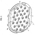
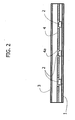
- Figures 1 and 2 of the annexed plates of drawings show, respectively, a perspective view and a schematic cross-sectional view of a back-lighting device for displays of a known type, which can be used, for example, for displays provided on dashboards of motor vehicles.
- Devices of this type comprise a substrate 1, on which a plurality of LED sources 2 of the SMD type are distributed, each of which is supplied by means of conductive paths (not illustrated) deposited on the substrate 1.
- a diffuser element 3 Set on top of the substrate 1 and of the LED sources 2 is a diffuser element 3 having a plane conformation.
- a back-diffuser 4 having a series of openings 4a in positions corresponding to the various LED sources 2.
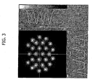
- Figure 3 of the annexed plates of drawings illustrates the typical illumination that can be obtained with the known device of Figures 1 and 2 and measured in a plane set immediately on top of the diffuser element 3.
- the resulting illuminance profile is not uniform but substantially presents the so-called "dot-effect".
- variable transmittance being maximum in the areas corresponding to a minimum illumination (for example, the areas located between two adjacent sources 2) and minimum in the areas corresponding to a maximum illumination (for example, the areas located in positions corresponding to the sources 2).
- Said patent describes an optical system designed to gather a substantially collimated beam of light to concentrate it in its focus.
- Said optical system is curved, with the concavity facing the focus, and is characterized by a saw-tooth profile operating in total internal reflection (TIR) for focusing the rays.
- TIR total internal reflection
- Said patent contemplates the embodiment in which a source of light is set in the focus, in which case the beam coming out of the optical system would be substantially collimated and parallel to the optical axis of said optical system.
- the optical system according to said embodiment is not able to guarantee a constant luminance on the surface of exit of the beam.
- the patent No. US5577493 illustrates an optical system that overcomes the problem of lack of uniformity of the patent previously referred to by setting between said source and the collimating lens an additional lens, designed to render the outcoming beam uniform. Said optical system maintains the curvature of the collimating lens with the concavity facing the source, and is applied to sources immersed in the additional lens.
- a device of the type indicated in the precharacterizing part of Claim 1 is known from the document No. WO 2007/036186 A .
- the device described in said document would in theory be able to illuminate a plane surface orthogonal to the optical axis of the source uniformly, for a limited area, but the divergence of the rays coming out of said optical system is in any case very wide, up to a maximum of approximately 180°, and is not controllable.
- the peripheral regions of the illuminated area to emit rays in a direction close to that of the optical axis of the system it would be necessary to introduce a diffuser with high divergence, with a consequent reduction in the overall efficiency of the system.
- the purpose of the present invention is to overcome the limitations of the known art, by providing a lighting device based upon semiconductor sources suitable for back-lighting dashboards for motor vehicles, that will be very compact, in particular with a very contained thickness, for example less than 20 mm, and that even so will be characterized by a substantially uniform outcoming light beam with a controlled divergence (for example, very small or else reduced in one direction and extended in the direction normal to the first).
- a lighting device based upon semiconductor sources suitable for back-lighting dashboards for motor vehicles that will be very compact, in particular with a very contained thickness, for example less than 20 mm, and that even so will be characterized by a substantially uniform outcoming light beam with a controlled divergence (for example, very small or else reduced in one direction and extended in the direction normal to the first).
- forming a purpose of the invention is the production of a lighting device based upon semiconductor sources suitable, for example, for back-lighting dashboards for motor vehicles that will make it possible to obtain:
- forming the subject of the present invention is a lighting device having the characteristics specified in Claim 1.
- the aforesaid predetermined distance is less than 20 mm.
- said distance can be in the region of 15 mm.
- the primary optical system and the secondary optical system are defined by two elements separate from one another.
- the primary optical system and the secondary optical system are defined by opposite surfaces of one and the same element.
- the invention applies both to the case of a single semiconductor source (LED or chip-LED) and to the case of a number of semiconductor sources (LEDs or chip-LEDs) designed to light up a predetermined area: in the latter case, the device forming the subject of the present patent is made up of the sum of a plurality of sub-devices substantially identical to one another and set alongside one another, each comprising a single semiconductor source associated to a primary optical system and a secondary optical system, said primary optical system being optimized so that the illuminance profile resulting therefrom, alongside the illuminance profile generated by the adjacent primary optical systems, forms a substantially uniform overall illuminance profile.
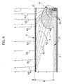
- the device f is optimized in the form of a back-lighter and comprises a substrate 1, set on which is a single light source 2 of a compact semiconductor type, for example of the SMD LED type or of the chip-LED type.
- the source 2 set on the substantially plane substrate 1 is immersed in a cap 5 constituted by a material having a refractive index higher than 1, for example resin, polycarbonate, polymethyl methacrylate, or glass.
- Said cap 5 constitutes a primary optical system for the respective LED source 2 and has an outer surface shaped so that the light emitted by the source immersed therein is refracted on the outer surface of the cap (see rays R1 and R2 in Figure 4 ) in such a way as to form, in a plane P-P ( Figure 4 ) substantially parallel to the substrate 1 and set at a predetermined distance D therefrom, typically not greater than 20 mm, a substantially uniform illuminance profile, by which it is meant that lighting-up of the plane P-P remains substantially constant from one point to another of the plane P-P.
- the surface in the plane P-P with substantially constant illuminance is linearly very extensive in a direction orthogonal to the principal axis of emission (i.e., in the horizontal direction in the figure), about at least twice the distance between the plane P-P and the source 2.
- Said cap 5 can be obtained using processes of a type in themselves known; for example:
- a secondary optical system is set, which, in the case of the embodiment illustrated in Figures 4 and 6 , is constituted by an element separate from the primary optical system 5, in the form of a plate 6.
- the plate 6 is made of a material having a refractive index higher than 1, for example polycarbonate or polymethyl methacrylate, of which at most one of the faces, for example the top face 6A (as viewed in Figure 10 ) is substantially plane and the other face 6B defines an optical surface, for example with circular symmetry, concentric with respect to the axis 7 passing through the centre of the cap 5 and of the emitting area of the source 2 and normal to the substrate 1.
- the optical surface 6b of the plate 6 is shaped so as to deviate the rays R2 ( Figure 4 ) into rays R3 that propagate in a direction such as to form a predetermined illuminance profile.
- said rays R3 can form a substantially collimated beam and hence originate an illuminance profile, such as the one represented in Figure 7 , where the semi-divergence is less than approximately 10°.
- the profile of the optical surface 6b can be:
- the Fresnel profile of the optical surface 6B is constituted by a combination of the previous two solutions; i.e., it is made up of direct regions and TIR regions so as to optimize the overall efficiency of the optical system.
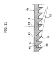
- the Fresnel profile can be obtained completely within the plate 6 constituting the secondary optical system, or else can be simplified by partly filling the grooves 6c of said Fresnel profile, that is ignoring the portions thereof that would be optically inactive, i.e., that would not be touched by the light rays emitted by the source and deviated by the primary optical system 5 (portions designated in Figure 11 by 6c).
- the marked thinning of the plate 6 in areas corresponding to said grooves 6c is eliminated, with considerable reduction in the aspect ratio of the profile of said secondary optical system, to the advantage of simplification of the production process.
- Figure 6 shows the advantages of the exemplary device in terms of uniformity of illuminance in a plane set downstream and in the proximity of the secondary optical system 6.
- the device comprises a substrate 1, distributed over which, in a way similar to what is illustrated in Figure 1 with reference to the known device, is a plurality of light sources 2 of a compact semiconductor type, for example of the SMD LED type or of the chip-LED type (see Figure 8 ).
- each source 2 set on the substantially plane substrate 1 is immersed in a cap 5 having a shape substantially resembling the first example described previously (see Figure 4 ).
- the difference with respect to the solution of Figure 4 lies in the fact that, in this case, the final profile is obtained by a plurality of sources 2.
- Each cap 5 in the solution of Figure 8 hence forms a primary optical system for the respective LED source 2 and has an outer surface shaped so that the light emitted by the source 2 immersed therein is refracted in an area corresponding to the outer surface of the cap 5 in such a way that the sum of the illuminance profiles formed by each cap 5 forms, in a plane P-P ( Figure 4 ) substantially parallel to the substrate 1 and set at a predetermined distance D therefrom, typically not greater than 20 mm, a substantially uniform illuminance profile. This means that the lighting of the plane P-P remains substantially constant from one point to another of the plane P-P (see Figure 9 ).
- Figure 18 shows a further variant, which amounts, for example, to the configuration exemplified in Figure 8 , where the multiplicity of caps 5 corresponding to the multiplicity of sources 2 is joined by a base-plate 15, the bottom surface of which is close to the substantially plane substrate 1 on which the multiplicity of sources 2 is deposited.
- Figure 5 illustrates a further example, in which, set on top of the substantially plane substrate 1, housing one or more sources 2, is a plate made of transparent material 10 (for example, polycarbonate or polymethyl methacrylate), the face 11 of which facing the substrate 1 has one or more cavities 12 (just one of which is visible in Figure 5 ), each in an area corresponding to a respective source 2, shaped like a solid of rotation about the axis 7, the surface of which has a profile shaped in such a way that the rays R1 of light emitted by the source 2 are refracted in rays R2 that propagate through the plate 10 until they form a substantially uniform illuminance profile in the proximity of the plane P-P parallel to the substrate 1 and set at a distance therefrom by a predetermined distance D.
- transparent material 10 for example, polycarbonate or polymethyl methacrylate
- said distance is less than 20 mm. Said distance may, for example, be 15 mm.
- the top surface 13 of the plate 10 is substantially parallel and coplanar to the plane P-P and defines an optical surface 13 shaped in a such a way as to deflect the rays R2 in rays R3 exiting according to a predetermined illuminance profile. Said optical surface 13 can be obtained:
- the optical system forming the subject of the present patent can be, for example, used as back-lighting system for dashboards.
- An example of mask for a dashboard is represented in Figure 12 :
- the central mobile pointer I is typically backlighted using a multiplicity of semiconductor sources 16, for example arranged as schematically represented in Figure 13 .
- the arrangement in Figure 13 is used for minimizing the lack of uniformity of lighting of the pointer during its rotation.
- the primary optical system (5, 12) can be used for forming an illuminance profile of the type represented in Figure 14 , constituted by:
- the primary optical system 5 has a shape such that the rays emitted by a single source 2 are deviated in such a way as to illuminate two regions 16 and 17 of the secondary optical system 6 uniformly, leaving the intermediate region 18 substantially in darkness.
- the secondary optical system has an appropriate optical profile, according to one of the embodiments described previously in the present patent, to form the desired illuminance profile.
- Said further embodiment of the present patent described with reference to the optical scheme presented in Figure 4 , can obviously be adapted to the optical scheme presented in Figure 5 .
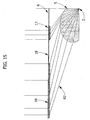
- the optical system can be used for providing an illuminance profile of the type represented in Figure 16 , constituted by:
- the primary optical system 5 has a form such as to direct the rays emitted by a single source 2 in such a way as to illuminate two regions 16 and 17 of the secondary optical system 6 uniformly, leaving the intermediate region 18 substantially in darkness.
- the secondary optical system has an appropriate optical profile, according to one of the embodiments described previously in the present patent, to form the desired illuminance profile.
- a multiplicity of optical systems 15 are provided in the plate 14, each of which is designed to gather the light emitted by a corresponding source 2 and direct it into a portion 18a of said region in darkness 18, in order to back-light a corresponding icon.
- Said region 18a can present a secondary optical system, appropriately shaped, according to what is described in the present patent, to form a given illuminance profile.
- the lighting device according to the invention is based upon the idea of providing, for each source, a primary optical system and a secondary optical system in order to obtain a substantially uniform outgoing light beam having a predetermined illuminance profile, minimizing the thickness of the device.
Landscapes
- Engineering & Computer Science (AREA)
- Mechanical Engineering (AREA)
- Physics & Mathematics (AREA)
- Transportation (AREA)
- Chemical & Material Sciences (AREA)
- Combustion & Propulsion (AREA)
- General Physics & Mathematics (AREA)
- Microelectronics & Electronic Packaging (AREA)
- Optics & Photonics (AREA)
- Planar Illumination Modules (AREA)
- Led Device Packages (AREA)
- Instrument Panels (AREA)
- Liquid Crystal (AREA)
- Details Of Measuring Devices (AREA)
Claims (21)
- Beleuchtungsvorrichtung, die für die Hintergrundbeleuchtung des Armaturenbrettes eines Kraftfahrzeugs verwendet wird, wobei die Vorrichtung enthält:- ein im wesentlichen ebenes Substrat (1);- wenigstens eine Halbleiter-LED- oder Chip-LED-Lichtquelle (2), die über das Substrat (1) verteilt ist und mit leitfähigen Versorgungswegen elektrisch verbunden ist;- primäre optische Einrichtungen (5; 12), die der Halbleiterquelle oder jeder Halbleiterquelle zugeordnet und dazu bestimmt sind, das Licht zu brechen, das von der Halbleiterquelle (2) emittiert wird; und- sekundäre optische Einrichtungen (6; 13), die die Divergenz der Lichtstrahlen steuern, die von den primären optischen Einrichtungen (5; 12) gebrochen werden,
wobei die Vorrichtung dadurch gekennzeichnet ist, dass:- die primären optischen Einrichtungen (5; 12) mit einer Oberfläche ausgestattet sind, die derart geformt ist, dass das Licht, das von einer einzelnen Halbleiterquelle (2) emittiert wird, derart gebrochen wird, dass eine im wesentlichen einheitliche Beleuchtung in einer Ebene (P-P) im wesentlichen parallel zu dem Substrat (1) und in einem Abstand erzeugt wird, der weniger als 20 mm von dem Substrat (1) entfernt ist, wobei die im wesentlichen einheitliche Beleuchtung für eine Oberflächenausdehnung erzeugt wird, die Bereiche enthält, die einer minimalen linearen Ausdehnung von etwa wenigstens dem Doppelten des Abstandes zwischen der Ebene (P-P) und der Quelle (2) entsprechen; und dadurch, dass:die sekundären optischen Einrichtungen (6; 13) in der Ebene (P-P) parallel zu dem Substrat (1) und im wesentlichen in den Bereichen angeordnet sind, die von den primären optischen Einrichtungen beleuchtet werden, um die Lichtstrahlen, die von den primären optischen Einrichtungen eintreffen, derart zu brechen, dass die Divergenz der Strahlen, die die sekundären optischen Einrichtungen verlassen, in einem gegebenen Winkel enthalten ist,- wobei die primären optischen Einrichtungen (5, 12) derart geformt sind, dass das Licht, das von einer einzigen Halbleiterquelle (2) emittiert wird, derart gebrochen wird, dass auf der Ebene (P-P) eine nicht kontinuierlich beleuchtete Oberfläche (16, 17) erzeugt wird, die eine Vielzahl separater Bereiche enthält, wobei jeder der Komponentenbereiche durch ein vorbestimmtes Beleuchtungsprofil gekennzeichnet ist,- wobei die separaten beleuchteten Bereiche wenigstens einen ersten, äußeren Bereich, der wie ein Ring geformt ist, um die Ziffernskala des Armaturenbrettes zu beleuchten, und einen zweiten, inneren Bereich enthalten, der wie ein Ring geformt ist, um einen Zeiger zu beleuchten. - Beleuchtungsvorrichtung nach Anspruch 1, dadurch gekennzeichnet, dass die primären optischen Einrichtungen und die sekundären optischen Einrichtungen durch zwei Elemente (5, 6) definiert sind, die voneinander getrennt sind.
- Beleuchtungsvorrichtung nach Anspruch 1, dadurch gekennzeichnet, dass die primären optischen Einrichtungen und die sekundären optischen Einrichtungen durch zwei Oberflächen (12, 13) ein und desselben Elementes (10) definiert sind.
- Beleuchtungsvorrichtung nach Anspruch 2, dadurch gekennzeichnet, dass die primären optischen Einrichtungen für jede Quelle (2) eine Kappe (5) enthalten, die aus einem Material besteht, das einen Brechungsindex von mehr als 1 hat, mit einer Außenoberfläche, die derart geformt ist, dass das Licht, das von der entsprechenden Quelle (2) emittiert wird, die darin enthalten ist, gebrochen wird und in der Ebene (P-P), die im wesentlichen parallel zum Substrat (1) ist, ein im wesentlichen einheitliches Beleuchtungsprofil ausbildet.
- Beleuchtungsvorrichtung nach Anspruch 4, dadurch gekennzeichnet, dass jede Kappe (5) direkt um die entsprechende Quelle (2) flüssig oder in Gelform mit Hilfe einer Form und anschließender thermischer Behandlung oder UV-Behandlung eingespritzt ist.
- Beleuchtungsvorrichtung nach Anspruch 4, dadurch gekennzeichnet, dass jede Kappe (5) vorab geformt und anschließend auf das Substrat (1) gesetzt wird, das die Quellen (2) aufnimmt, wobei jede Kappe (5) ihren eigenen Bodenflächenhohlraum (14) hat, der die entsprechende Quelle (2) aufnimmt.
- Beleuchtungsvorrichtung nach Anspruch 6, dadurch gekennzeichnet, dass der Hohlraum (14), der in der Bodenfläche der Kappe ausgebildet ist, eine im wesentlichen halbkugelförmige Form hat und sich sein Zentrum auf der Achse befindet, die durch das Zentrum des Emittierbereiches der Quelle (2) und orthogonal zu dem Substrat (1) verläuft.
- Beleuchtungsvorrichtung nach Anspruch 6, dadurch gekennzeichnet, dass der Abstand zwischen der Quelle (2) und der Oberfläche des Hohlraumes (14), der in der Bodenfläche der Kappe (5) ausgebildet ist, mit einem Material gefüllt ist, das einen Brechungsindex hat, der dem der Kappe gleichkommt.
- Beleuchtungsvorrichtung nach Anspruch 6, dadurch gekennzeichnet, dass die Oberfläche des Hohlraums (14) etwa so geformt ist, dass die Position der virtuellen Quelle (2') der Strahlen (R1), die die Kappe (5) durchlaufen, vorbestimmt ist.
- Beleuchtungsvorrichtung nach Anspruch 2, dadurch gekennzeichnet, dass die sekundären optischen Einrichtungen aus einer Platte (6) bestehen, die aus einem Material gefertigt ist, das einen Brechungsindex größer 1 hat, und eine erste im wesentlichen plane Fläche (6a) sowie eine zweite Fläche (6b) aufweist, die eine optische Oberfläche bildet, die dazu bestimmt ist, den Strahl einfallender Strahlen gemäß einem vorbestimmten Beleuchtungsprofil abzulenken.
- Beleuchtungsvorrichtung nach Anspruch 10, dadurch gekennzeichnet, dass die optische Oberfläche (6b) ein Fresnel-Profil definiert, das derart geformt ist, dass es eine Brechung des einfallenden Lichtes innerhalb des Profils bestimmt, wobei die Lichtstrahlen, die von dem Fresnel-Profil gebrochen werden, anschließend einer weiteren Brechung an dem Ausgang aus den sekundären optischen Einrichtungen unterzogen werden.
- Beleuchtungsvorrichtung nach Anspruch 10, dadurch gekennzeichnet, dass die optische Oberfläche (6b) ein Fresnel-Profil definiert, das so geformt ist, dass eine Brechung des einfallenden Strahls und anschließend eine innere Totalreflexion desselben bestimmt wird, wobei die Lichtstrahlen einer anschließenden Brechung an dem Ausgang aus dem optischen System unterzogen werden.
- Beleuchtungsvorrichtung nach Anspruch 10, dadurch gekennzeichnet, dass das Fresnel-Profil derart geformt ist, dass es Bereiche enthält, die dazu bestimmt sind, eine Brechung des einfallenden Strahls zu bestimmen, und Bereiche, die dazu bestimmt sind, eine Brechung des einfallenden Strahls und anschließend eine innere Totalreflexion desselben zu bestimmen, wobei die Lichtstrahlen einer anschließenden Brechung an dem Ausgang aus dem optischen System unterzogen werden.
- Beleuchtungsvorrichtung nach Anspruch 10, dadurch gekennzeichnet, dass die optische Oberfläche (6b) einem theoretischen Fresnel-Profil mit Ausnahme optisch inaktiver Abschnitte der Platte (6) insoweit entspricht, als sie nicht von den Lichtstrahlen berührt wird, die von der Quelle emittiert und von den primären optischen Einrichtungen abgelenkt werden, wobei die Dicke der Platte im Bezug auf das theoretische Fresnel-Profil erhöht ist, um das Bildseitenverhältnis des finalen Profils der Platte zu verringern.
- Beleuchtungsvorrichtung nach Anspruch 3, dadurch gekennzeichnet, dass die primären optischen Einrichtungen und die sekundären optischen Einrichtungen durch die gegenüberliegenden Oberflächen (11, 13) einer Platte definiert sind, die aus einem transparenten Material (10) besteht, das auf der Oberseite des Substrates (1) angeordnet ist.
- Beleuchtungsvorrichtung nach Anspruch 15, dadurch gekennzeichnet, dass auf der Fläche der Platte (10), die dem Substrat (1) zugewandt ist, eine Vielzahl von Hohlräumen (12) ausgebildet ist, wobei jeder Hohlraum einer jeweiligen Quelle (2) entspricht und wie ein Rotationskörper um eine Achse (7) geformt ist, die orthogonal zu dem Substrat und durch das Zentrum (2) der Quelle verläuft, wobei die Oberfläche des Hohlraums (12) derart geformt ist, dass das Licht, das von der Quelle emittiert wird, von der Oberfläche gebrochen wird, um ein im wesentlichen einheitliches Beleuchtungsprofil in der Nähe der zweiten Fläche (13) der Platte (10) zu definieren.
- Beleuchtungsvorrichtung nach Anspruch 16, dadurch gekennzeichnet, dass auf der Fläche der Platte (10), die jener gegenüberliegt, die den Quellen (2) zugewandt ist, eine optische Oberfläche (13) definiert ist, die dazu bestimmt ist, den Strahl ausgehender Strahlen gemäß einem vorbestimmten Beleuchtungsprofil abzulenken, das gemäß einem Fresnel-Profil mit Kreissymmetrie geformt ist, wobei das Zentrum auf der Achse liegt, die orthogonal zu dem Substrat (1) und durch das Zentrum des Emissionsbereiches der entsprechenden Quelle (2) verläuft.
- Beleuchtungsvorrichtung nach Anspruch 4, dadurch gekennzeichnet, dass die primären optischen Einrichtungen aus einer Vielzahl von Kappen (5) bestehen, die miteinander durch eine Platte verbunden sind, die aus einem transparenten Material (19) besteht, das auf dem Substrat (1) ruht.
- Vorrichtung nach Anspruch 1, dadurch gekennzeichnet, dass die separaten beleuchteten Bereiche darüber hinaus eine Vielzahl dritter Bereiche enthalten, die in Umfangsrichtung zwischen dem ersten Bereich und dem zweiten Bereich verteilt sind, um eine Vielzahl von Symbolen auf dem Armaturenbrett zu beleuchten.
- Vorrichtung nach Anspruch 19, dadurch gekennzeichnet, dass die primären optischen Einrichtungen eine Vielzahl von Zusatz-LED-Quellen (16) zum Beleuchten der dritten Bereiche enthalten.
- Vorrichtung nach Anspruch 1, dadurch gekennzeichnet, dass die Divergenz der Strahlen, die die sekundären optischen Einrichtungen (5; 12) verlassen, nicht größer als 20° ist.
Priority Applications (1)
| Application Number | Priority Date | Filing Date | Title |
|---|---|---|---|
| EP07121961A EP2015126B1 (de) | 2007-07-10 | 2007-11-30 | Leuchtdiode mit einer Strahlformungsvorrichtung zur Hintergrundbeleuchtung einer Instrumententafel |
Applications Claiming Priority (2)
| Application Number | Priority Date | Filing Date | Title |
|---|---|---|---|
| EP07425427A EP2015127A1 (de) | 2007-07-10 | 2007-07-10 | Leuchtdiode mit Strahlformungsvorrichtung für die Hintergrundbeleuchtung einer Anzeigevorrichtung oder einer Instrumententafel |
| EP07121961A EP2015126B1 (de) | 2007-07-10 | 2007-11-30 | Leuchtdiode mit einer Strahlformungsvorrichtung zur Hintergrundbeleuchtung einer Instrumententafel |
Publications (2)
| Publication Number | Publication Date |
|---|---|
| EP2015126A1 EP2015126A1 (de) | 2009-01-14 |
| EP2015126B1 true EP2015126B1 (de) | 2011-01-26 |
Family
ID=38626413
Family Applications (2)
| Application Number | Title | Priority Date | Filing Date |
|---|---|---|---|
| EP07425427A Withdrawn EP2015127A1 (de) | 2007-07-10 | 2007-07-10 | Leuchtdiode mit Strahlformungsvorrichtung für die Hintergrundbeleuchtung einer Anzeigevorrichtung oder einer Instrumententafel |
| EP07121961A Not-in-force EP2015126B1 (de) | 2007-07-10 | 2007-11-30 | Leuchtdiode mit einer Strahlformungsvorrichtung zur Hintergrundbeleuchtung einer Instrumententafel |
Family Applications Before (1)
| Application Number | Title | Priority Date | Filing Date |
|---|---|---|---|
| EP07425427A Withdrawn EP2015127A1 (de) | 2007-07-10 | 2007-07-10 | Leuchtdiode mit Strahlformungsvorrichtung für die Hintergrundbeleuchtung einer Anzeigevorrichtung oder einer Instrumententafel |
Country Status (3)
| Country | Link |
|---|---|
| EP (2) | EP2015127A1 (de) |
| AT (1) | ATE497188T1 (de) |
| DE (1) | DE602007012227D1 (de) |
Families Citing this family (7)
| Publication number | Priority date | Publication date | Assignee | Title |
|---|---|---|---|---|
| DE102010054449B4 (de) * | 2010-12-14 | 2018-10-11 | Trw Automotive Electronics & Components Gmbh | Optische Projektionsvorrichtung |
| JP5642631B2 (ja) * | 2011-07-06 | 2014-12-17 | カルソニックカンセイ株式会社 | 計器照明装置 |
| JP5917180B2 (ja) * | 2012-02-09 | 2016-05-11 | ミネベア株式会社 | 面状照明装置 |
| AT514573B1 (de) * | 2013-08-27 | 2015-02-15 | Univ Wien Tech | Lichtlenkvorrichtung und Beleuchtungseinheit mit einer solchen Lichtlenkvorrichtung |
| DE102014103849B4 (de) * | 2014-03-20 | 2020-08-06 | Bcs Automotive Interface Solutions Gmbh | Linsenplatte |
| TW201727275A (zh) * | 2015-11-05 | 2017-08-01 | 康寧公司 | 具有菲涅耳光學系統的發光單元以及使用該發光單元的發光裝置及顯示系統 |
| US11623562B2 (en) | 2020-01-15 | 2023-04-11 | Aptiv Technologies Limited | Light control apparatus and method |
Family Cites Families (9)
| Publication number | Priority date | Publication date | Assignee | Title |
|---|---|---|---|---|
| US5148317A (en) * | 1991-06-24 | 1992-09-15 | The United States Of America As Represented By The Secretary Of The Air Force | Diffractive optical element for collimating and redistributing Gaussian input beam |
| US5404869A (en) | 1992-04-16 | 1995-04-11 | Tir Technologies, Inc. | Faceted totally internally reflecting lens with individually curved faces on facets |
| US5703612A (en) * | 1995-01-20 | 1997-12-30 | Nu-Tech & Engineering, Inc. | Illuminated pointer for an analog gauge and related method of use and manufacture |
| PT806039E (pt) * | 1995-08-30 | 2002-10-31 | Samsung Electronics Co Ltd | Dispositivo de lente e aparelho de captacao optica que usa esse dispositivo |
| ES2157846B1 (es) * | 1999-12-02 | 2002-03-01 | Univ Madrid Politecnica | Dispositivo con lente discontinua de reflexion total interna y dioptrico asferico para concentracion o colimacion de energia radiante. |
| US20050286145A1 (en) * | 2004-06-25 | 2005-12-29 | Swarco Futurit Verkehrssignalsysteme Ges.M.B.H. | Invention concerning a condensor lens |
| KR101080355B1 (ko) * | 2004-10-18 | 2011-11-04 | 삼성전자주식회사 | 발광다이오드와 그 렌즈 |
| JP2007079528A (ja) * | 2005-08-16 | 2007-03-29 | Toshiba Corp | 照明装置及び照明装置付撮像装置 |
| DE102005061798A1 (de) * | 2005-09-30 | 2007-04-05 | Osram Opto Semiconductors Gmbh | Beleuchtungsanordnung |
-
2007
- 2007-07-10 EP EP07425427A patent/EP2015127A1/de not_active Withdrawn
- 2007-11-30 AT AT07121961T patent/ATE497188T1/de not_active IP Right Cessation
- 2007-11-30 DE DE602007012227T patent/DE602007012227D1/de active Active
- 2007-11-30 EP EP07121961A patent/EP2015126B1/de not_active Not-in-force
Also Published As
| Publication number | Publication date |
|---|---|
| EP2015126A1 (de) | 2009-01-14 |
| ATE497188T1 (de) | 2011-02-15 |
| EP2015127A1 (de) | 2009-01-14 |
| DE602007012227D1 (de) | 2011-03-10 |
Similar Documents
| Publication | Publication Date | Title |
|---|---|---|
| US7218830B2 (en) | Surface illuminator using point light source | |
| JP4655155B2 (ja) | 発光装置および画像表示装置 | |
| EP2015126A1 (de) | Leuchtdiode mit einer Strahlformungsvorrichtung zur Hintergrundbeleuchtung einer Instrumententafel | |
| US20130208502A1 (en) | Spread illuminating apparatus | |
| JP2005135844A (ja) | 光学素子及びバックライト装置 | |
| EP2578931B1 (de) | Oberflächen-emittierende led-abdeckung, beleuchtungsvorrichtung und anzeigevorrichtung | |
| KR20050041965A (ko) | 도광판 및 백라이트 장치 | |
| US9310546B2 (en) | Backlight unit and display device having the same | |
| EP2279374B1 (de) | Optisches element für asymmetrische lichtverteilung | |
| KR20090009968A (ko) | 조광기능을 가진 입력장치 | |
| JP2013062074A (ja) | 車両用灯具のコンビネーションランプ | |
| KR20150117510A (ko) | 광학 부재, 및 이를 포함하는 백라이트 유닛 | |
| CN109061942B (zh) | 侧入式背光模组及显示装置 | |
| KR102467552B1 (ko) | 자동차 계기판용 글로우 링 | |
| JP2005302485A (ja) | 面状照明装置 | |
| JP4755165B2 (ja) | バックライトモジュール | |
| CN115769020A (zh) | 面状照明装置 | |
| JP4360862B2 (ja) | 導光板ユニットならびに平面照明装置 | |
| JP3936871B2 (ja) | 導光ブロック | |
| CN113260908B (zh) | 显示装置、照明装置、导光部件及导光构造 | |
| JPH1172787A (ja) | 照明装置、液晶表示装置及び電子機器 | |
| KR101488382B1 (ko) | 측면 방출형 발광다이오드용 렌즈, 이를 구비하는 백라이트유닛 및 표시장치 | |
| KR101398186B1 (ko) | 측면 방출형 발광다이오드용 렌즈, 이를 구비하는 백라이트유닛 및 표시장치 | |
| CN120202428A (zh) | 光学元件、光学系统和车辆窗板和/或窗板层压件 | |
| CN115349101B (zh) | 照明装置 |
Legal Events
| Date | Code | Title | Description |
|---|---|---|---|
| PUAI | Public reference made under article 153(3) epc to a published international application that has entered the european phase |
Free format text: ORIGINAL CODE: 0009012 |
|
| 17P | Request for examination filed |
Effective date: 20081111 |
|
| AK | Designated contracting states |
Kind code of ref document: A1 Designated state(s): AT BE BG CH CY CZ DE DK EE ES FI FR GB GR HU IE IS IT LI LT LU LV MC MT NL PL PT RO SE SI SK TR |
|
| AX | Request for extension of the european patent |
Extension state: AL BA HR MK RS |
|
| 17Q | First examination report despatched |
Effective date: 20090722 |
|
| AKX | Designation fees paid |
Designated state(s): AT BE BG CH CY CZ DE DK EE ES FI FR GB GR HU IE IS IT LI LT LU LV MC MT NL PL PT RO SE SI SK TR |
|
| GRAP | Despatch of communication of intention to grant a patent |
Free format text: ORIGINAL CODE: EPIDOSNIGR1 |
|
| RIN1 | Information on inventor provided before grant (corrected) |
Inventor name: BERNARD, STEFANO Inventor name: BOLLEA, DENIS Inventor name: INNOCENTI, GIANFRANCO |
|
| GRAS | Grant fee paid |
Free format text: ORIGINAL CODE: EPIDOSNIGR3 |
|
| GRAA | (expected) grant |
Free format text: ORIGINAL CODE: 0009210 |
|
| AK | Designated contracting states |
Kind code of ref document: B1 Designated state(s): AT BE BG CH CY CZ DE DK EE ES FI FR GB GR HU IE IS IT LI LT LU LV MC MT NL PL PT RO SE SI SK TR |
|
| REG | Reference to a national code |
Ref country code: GB Ref legal event code: FG4D |
|
| REG | Reference to a national code |
Ref country code: CH Ref legal event code: EP |
|
| REG | Reference to a national code |
Ref country code: IE Ref legal event code: FG4D |
|
| REF | Corresponds to: |
Ref document number: 602007012227 Country of ref document: DE Date of ref document: 20110310 Kind code of ref document: P |
|
| REG | Reference to a national code |
Ref country code: DE Ref legal event code: R096 Ref document number: 602007012227 Country of ref document: DE Effective date: 20110310 |
|
| REG | Reference to a national code |
Ref country code: NL Ref legal event code: VDEP Effective date: 20110126 |
|
| LTIE | Lt: invalidation of european patent or patent extension |
Effective date: 20110126 |
|
| PG25 | Lapsed in a contracting state [announced via postgrant information from national office to epo] |
Ref country code: ES Free format text: LAPSE BECAUSE OF FAILURE TO SUBMIT A TRANSLATION OF THE DESCRIPTION OR TO PAY THE FEE WITHIN THE PRESCRIBED TIME-LIMIT Effective date: 20110507 Ref country code: LT Free format text: LAPSE BECAUSE OF FAILURE TO SUBMIT A TRANSLATION OF THE DESCRIPTION OR TO PAY THE FEE WITHIN THE PRESCRIBED TIME-LIMIT Effective date: 20110126 Ref country code: SE Free format text: LAPSE BECAUSE OF FAILURE TO SUBMIT A TRANSLATION OF THE DESCRIPTION OR TO PAY THE FEE WITHIN THE PRESCRIBED TIME-LIMIT Effective date: 20110126 Ref country code: PT Free format text: LAPSE BECAUSE OF FAILURE TO SUBMIT A TRANSLATION OF THE DESCRIPTION OR TO PAY THE FEE WITHIN THE PRESCRIBED TIME-LIMIT Effective date: 20110526 Ref country code: LV Free format text: LAPSE BECAUSE OF FAILURE TO SUBMIT A TRANSLATION OF THE DESCRIPTION OR TO PAY THE FEE WITHIN THE PRESCRIBED TIME-LIMIT Effective date: 20110126 Ref country code: IS Free format text: LAPSE BECAUSE OF FAILURE TO SUBMIT A TRANSLATION OF THE DESCRIPTION OR TO PAY THE FEE WITHIN THE PRESCRIBED TIME-LIMIT Effective date: 20110526 Ref country code: GR Free format text: LAPSE BECAUSE OF FAILURE TO SUBMIT A TRANSLATION OF THE DESCRIPTION OR TO PAY THE FEE WITHIN THE PRESCRIBED TIME-LIMIT Effective date: 20110427 |
|
| PG25 | Lapsed in a contracting state [announced via postgrant information from national office to epo] |
Ref country code: FI Free format text: LAPSE BECAUSE OF FAILURE TO SUBMIT A TRANSLATION OF THE DESCRIPTION OR TO PAY THE FEE WITHIN THE PRESCRIBED TIME-LIMIT Effective date: 20110126 Ref country code: BE Free format text: LAPSE BECAUSE OF FAILURE TO SUBMIT A TRANSLATION OF THE DESCRIPTION OR TO PAY THE FEE WITHIN THE PRESCRIBED TIME-LIMIT Effective date: 20110126 Ref country code: SI Free format text: LAPSE BECAUSE OF FAILURE TO SUBMIT A TRANSLATION OF THE DESCRIPTION OR TO PAY THE FEE WITHIN THE PRESCRIBED TIME-LIMIT Effective date: 20110126 Ref country code: NL Free format text: LAPSE BECAUSE OF FAILURE TO SUBMIT A TRANSLATION OF THE DESCRIPTION OR TO PAY THE FEE WITHIN THE PRESCRIBED TIME-LIMIT Effective date: 20110126 Ref country code: AT Free format text: LAPSE BECAUSE OF FAILURE TO SUBMIT A TRANSLATION OF THE DESCRIPTION OR TO PAY THE FEE WITHIN THE PRESCRIBED TIME-LIMIT Effective date: 20110126 Ref country code: BG Free format text: LAPSE BECAUSE OF FAILURE TO SUBMIT A TRANSLATION OF THE DESCRIPTION OR TO PAY THE FEE WITHIN THE PRESCRIBED TIME-LIMIT Effective date: 20110426 Ref country code: CY Free format text: LAPSE BECAUSE OF FAILURE TO SUBMIT A TRANSLATION OF THE DESCRIPTION OR TO PAY THE FEE WITHIN THE PRESCRIBED TIME-LIMIT Effective date: 20110126 Ref country code: PL Free format text: LAPSE BECAUSE OF FAILURE TO SUBMIT A TRANSLATION OF THE DESCRIPTION OR TO PAY THE FEE WITHIN THE PRESCRIBED TIME-LIMIT Effective date: 20110126 |
|
| PG25 | Lapsed in a contracting state [announced via postgrant information from national office to epo] |
Ref country code: DK Free format text: LAPSE BECAUSE OF FAILURE TO SUBMIT A TRANSLATION OF THE DESCRIPTION OR TO PAY THE FEE WITHIN THE PRESCRIBED TIME-LIMIT Effective date: 20110126 Ref country code: EE Free format text: LAPSE BECAUSE OF FAILURE TO SUBMIT A TRANSLATION OF THE DESCRIPTION OR TO PAY THE FEE WITHIN THE PRESCRIBED TIME-LIMIT Effective date: 20110126 |
|
| PG25 | Lapsed in a contracting state [announced via postgrant information from national office to epo] |
Ref country code: CZ Free format text: LAPSE BECAUSE OF FAILURE TO SUBMIT A TRANSLATION OF THE DESCRIPTION OR TO PAY THE FEE WITHIN THE PRESCRIBED TIME-LIMIT Effective date: 20110126 Ref country code: SK Free format text: LAPSE BECAUSE OF FAILURE TO SUBMIT A TRANSLATION OF THE DESCRIPTION OR TO PAY THE FEE WITHIN THE PRESCRIBED TIME-LIMIT Effective date: 20110126 Ref country code: RO Free format text: LAPSE BECAUSE OF FAILURE TO SUBMIT A TRANSLATION OF THE DESCRIPTION OR TO PAY THE FEE WITHIN THE PRESCRIBED TIME-LIMIT Effective date: 20110126 |
|
| PLBE | No opposition filed within time limit |
Free format text: ORIGINAL CODE: 0009261 |
|
| STAA | Information on the status of an ep patent application or granted ep patent |
Free format text: STATUS: NO OPPOSITION FILED WITHIN TIME LIMIT |
|
| 26N | No opposition filed |
Effective date: 20111027 |
|
| REG | Reference to a national code |
Ref country code: DE Ref legal event code: R097 Ref document number: 602007012227 Country of ref document: DE Effective date: 20111027 |
|
| PG25 | Lapsed in a contracting state [announced via postgrant information from national office to epo] |
Ref country code: MC Free format text: LAPSE BECAUSE OF NON-PAYMENT OF DUE FEES Effective date: 20111130 |
|
| REG | Reference to a national code |
Ref country code: CH Ref legal event code: PL |
|
| GBPC | Gb: european patent ceased through non-payment of renewal fee |
Effective date: 20111130 |
|
| PG25 | Lapsed in a contracting state [announced via postgrant information from national office to epo] |
Ref country code: LI Free format text: LAPSE BECAUSE OF NON-PAYMENT OF DUE FEES Effective date: 20111130 Ref country code: CH Free format text: LAPSE BECAUSE OF NON-PAYMENT OF DUE FEES Effective date: 20111130 |
|
| REG | Reference to a national code |
Ref country code: IE Ref legal event code: MM4A |
|
| PG25 | Lapsed in a contracting state [announced via postgrant information from national office to epo] |
Ref country code: GB Free format text: LAPSE BECAUSE OF NON-PAYMENT OF DUE FEES Effective date: 20111130 Ref country code: IE Free format text: LAPSE BECAUSE OF NON-PAYMENT OF DUE FEES Effective date: 20111130 |
|
| PG25 | Lapsed in a contracting state [announced via postgrant information from national office to epo] |
Ref country code: MT Free format text: LAPSE BECAUSE OF FAILURE TO SUBMIT A TRANSLATION OF THE DESCRIPTION OR TO PAY THE FEE WITHIN THE PRESCRIBED TIME-LIMIT Effective date: 20110126 |
|
| PG25 | Lapsed in a contracting state [announced via postgrant information from national office to epo] |
Ref country code: LU Free format text: LAPSE BECAUSE OF NON-PAYMENT OF DUE FEES Effective date: 20111130 |
|
| PG25 | Lapsed in a contracting state [announced via postgrant information from national office to epo] |
Ref country code: TR Free format text: LAPSE BECAUSE OF FAILURE TO SUBMIT A TRANSLATION OF THE DESCRIPTION OR TO PAY THE FEE WITHIN THE PRESCRIBED TIME-LIMIT Effective date: 20110126 |
|
| PG25 | Lapsed in a contracting state [announced via postgrant information from national office to epo] |
Ref country code: HU Free format text: LAPSE BECAUSE OF FAILURE TO SUBMIT A TRANSLATION OF THE DESCRIPTION OR TO PAY THE FEE WITHIN THE PRESCRIBED TIME-LIMIT Effective date: 20110126 |
|
| REG | Reference to a national code |
Ref country code: FR Ref legal event code: PLFP Year of fee payment: 9 |
|
| REG | Reference to a national code |
Ref country code: FR Ref legal event code: PLFP Year of fee payment: 10 |
|
| REG | Reference to a national code |
Ref country code: FR Ref legal event code: PLFP Year of fee payment: 11 |
|
| PGFP | Annual fee paid to national office [announced via postgrant information from national office to epo] |
Ref country code: FR Payment date: 20171129 Year of fee payment: 11 |
|
| PGFP | Annual fee paid to national office [announced via postgrant information from national office to epo] |
Ref country code: IT Payment date: 20171116 Year of fee payment: 11 |
|
| PGFP | Annual fee paid to national office [announced via postgrant information from national office to epo] |
Ref country code: DE Payment date: 20180131 Year of fee payment: 11 |
|
| REG | Reference to a national code |
Ref country code: DE Ref legal event code: R119 Ref document number: 602007012227 Country of ref document: DE |
|
| PG25 | Lapsed in a contracting state [announced via postgrant information from national office to epo] |
Ref country code: DE Free format text: LAPSE BECAUSE OF NON-PAYMENT OF DUE FEES Effective date: 20190601 Ref country code: IT Free format text: LAPSE BECAUSE OF NON-PAYMENT OF DUE FEES Effective date: 20181130 Ref country code: FR Free format text: LAPSE BECAUSE OF NON-PAYMENT OF DUE FEES Effective date: 20181130 |