EP2015307B1 - Magnetoresistive Vorrichtung - Google Patents
Magnetoresistive Vorrichtung Download PDFInfo
- Publication number
- EP2015307B1 EP2015307B1 EP07112497.8A EP07112497A EP2015307B1 EP 2015307 B1 EP2015307 B1 EP 2015307B1 EP 07112497 A EP07112497 A EP 07112497A EP 2015307 B1 EP2015307 B1 EP 2015307B1
- Authority
- EP
- European Patent Office
- Prior art keywords
- ferromagnetic
- pulse
- magnetisation
- applying
- layer
- Prior art date
- Legal status (The legal status is an assumption and is not a legal conclusion. Google has not performed a legal analysis and makes no representation as to the accuracy of the status listed.)
- Ceased
Links
- 230000005291 magnetic effect Effects 0.000 claims description 126
- 230000005294 ferromagnetic effect Effects 0.000 claims description 100
- 230000005415 magnetization Effects 0.000 claims description 48
- 230000005684 electric field Effects 0.000 claims description 37
- 238000000034 method Methods 0.000 claims description 31
- 229910052748 manganese Inorganic materials 0.000 claims description 27
- 230000008859 change Effects 0.000 claims description 20
- 230000004888 barrier function Effects 0.000 claims description 16
- 238000012546 transfer Methods 0.000 claims description 16
- 238000009826 distribution Methods 0.000 claims description 14
- 239000004065 semiconductor Substances 0.000 claims description 14
- 239000002800 charge carrier Substances 0.000 claims description 13
- 239000011572 manganese Substances 0.000 description 52
- JBRZTFJDHDCESZ-UHFFFAOYSA-N AsGa Chemical compound [As]#[Ga] JBRZTFJDHDCESZ-UHFFFAOYSA-N 0.000 description 38
- 229910001218 Gallium arsenide Inorganic materials 0.000 description 33
- 239000000758 substrate Substances 0.000 description 27
- MDPILPRLPQYEEN-UHFFFAOYSA-N aluminium arsenide Chemical compound [As]#[Al] MDPILPRLPQYEEN-UHFFFAOYSA-N 0.000 description 16
- 230000000694 effects Effects 0.000 description 15
- 238000005259 measurement Methods 0.000 description 15
- 239000010931 gold Substances 0.000 description 7
- 229910052738 indium Inorganic materials 0.000 description 7
- APFVFJFRJDLVQX-UHFFFAOYSA-N indium atom Chemical compound [In] APFVFJFRJDLVQX-UHFFFAOYSA-N 0.000 description 7
- 238000000059 patterning Methods 0.000 description 7
- 238000001020 plasma etching Methods 0.000 description 6
- 239000013590 bulk material Substances 0.000 description 5
- 238000000609 electron-beam lithography Methods 0.000 description 5
- 238000004088 simulation Methods 0.000 description 5
- 229910000530 Gallium indium arsenide Inorganic materials 0.000 description 4
- 238000004364 calculation method Methods 0.000 description 4
- 239000013078 crystal Substances 0.000 description 4
- 238000013016 damping Methods 0.000 description 4
- 239000003302 ferromagnetic material Substances 0.000 description 4
- 239000000463 material Substances 0.000 description 4
- PWHULOQIROXLJO-UHFFFAOYSA-N Manganese Chemical compound [Mn] PWHULOQIROXLJO-UHFFFAOYSA-N 0.000 description 3
- 230000002547 anomalous effect Effects 0.000 description 3
- 230000008901 benefit Effects 0.000 description 3
- 230000008878 coupling Effects 0.000 description 3
- 238000010168 coupling process Methods 0.000 description 3
- 238000005859 coupling reaction Methods 0.000 description 3
- 230000007423 decrease Effects 0.000 description 3
- 230000001419 dependent effect Effects 0.000 description 3
- 239000010408 film Substances 0.000 description 3
- 230000006870 function Effects 0.000 description 3
- PCHJSUWPFVWCPO-UHFFFAOYSA-N gold Chemical compound [Au] PCHJSUWPFVWCPO-UHFFFAOYSA-N 0.000 description 3
- 229910052737 gold Inorganic materials 0.000 description 3
- 230000001965 increasing effect Effects 0.000 description 3
- 238000004519 manufacturing process Methods 0.000 description 3
- 229910052751 metal Inorganic materials 0.000 description 3
- 239000002184 metal Substances 0.000 description 3
- 239000000203 mixture Substances 0.000 description 3
- 230000010355 oscillation Effects 0.000 description 3
- 230000005355 Hall effect Effects 0.000 description 2
- XEEYBQQBJWHFJM-UHFFFAOYSA-N Iron Chemical compound [Fe] XEEYBQQBJWHFJM-UHFFFAOYSA-N 0.000 description 2
- KFZMGEQAYNKOFK-UHFFFAOYSA-N Isopropanol Chemical compound CC(C)O KFZMGEQAYNKOFK-UHFFFAOYSA-N 0.000 description 2
- 229910003910 SiCl4 Inorganic materials 0.000 description 2
- KXNLCSXBJCPWGL-UHFFFAOYSA-N [Ga].[As].[In] Chemical compound [Ga].[As].[In] KXNLCSXBJCPWGL-UHFFFAOYSA-N 0.000 description 2
- 229910052785 arsenic Inorganic materials 0.000 description 2
- 239000000969 carrier Substances 0.000 description 2
- 229910003460 diamond Inorganic materials 0.000 description 2
- 239000010432 diamond Substances 0.000 description 2
- 238000010894 electron beam technology Methods 0.000 description 2
- 230000001747 exhibiting effect Effects 0.000 description 2
- VFLRPJJARDQRAC-UHFFFAOYSA-N gallium manganese Chemical compound [Mn].[Ga] VFLRPJJARDQRAC-UHFFFAOYSA-N 0.000 description 2
- 239000003292 glue Substances 0.000 description 2
- BHEPBYXIRTUNPN-UHFFFAOYSA-N hydridophosphorus(.) (triplet) Chemical compound [PH] BHEPBYXIRTUNPN-UHFFFAOYSA-N 0.000 description 2
- 238000010884 ion-beam technique Methods 0.000 description 2
- 238000002955 isolation Methods 0.000 description 2
- 229910052451 lead zirconate titanate Inorganic materials 0.000 description 2
- 150000002739 metals Chemical class 0.000 description 2
- 238000001451 molecular beam epitaxy Methods 0.000 description 2
- 239000004926 polymethyl methacrylate Substances 0.000 description 2
- 230000008569 process Effects 0.000 description 2
- 230000009467 reduction Effects 0.000 description 2
- FDNAPBUWERUEDA-UHFFFAOYSA-N silicon tetrachloride Chemical compound Cl[Si](Cl)(Cl)Cl FDNAPBUWERUEDA-UHFFFAOYSA-N 0.000 description 2
- 230000007704 transition Effects 0.000 description 2
- 230000001960 triggered effect Effects 0.000 description 2
- -1 (Ga Substances 0.000 description 1
- 229910000531 Co alloy Inorganic materials 0.000 description 1
- 229910018936 CoPd Inorganic materials 0.000 description 1
- 229910018979 CoPt Inorganic materials 0.000 description 1
- 229910000640 Fe alloy Inorganic materials 0.000 description 1
- 229910005335 FePt Inorganic materials 0.000 description 1
- NTIZESTWPVYFNL-UHFFFAOYSA-N Methyl isobutyl ketone Chemical compound CC(C)CC(C)=O NTIZESTWPVYFNL-UHFFFAOYSA-N 0.000 description 1
- UIHCLUNTQKBZGK-UHFFFAOYSA-N Methyl isobutyl ketone Natural products CCC(C)C(C)=O UIHCLUNTQKBZGK-UHFFFAOYSA-N 0.000 description 1
- 229910000990 Ni alloy Inorganic materials 0.000 description 1
- 239000004642 Polyimide Substances 0.000 description 1
- 229910020776 SixNy Inorganic materials 0.000 description 1
- 239000000370 acceptor Substances 0.000 description 1
- 230000009471 action Effects 0.000 description 1
- 229910045601 alloy Inorganic materials 0.000 description 1
- 239000000956 alloy Substances 0.000 description 1
- RQNWIZPPADIBDY-UHFFFAOYSA-N arsenic atom Chemical class [As] RQNWIZPPADIBDY-UHFFFAOYSA-N 0.000 description 1
- 238000012512 characterization method Methods 0.000 description 1
- 229910017052 cobalt Inorganic materials 0.000 description 1
- 239000010941 cobalt Substances 0.000 description 1
- GUTLYIVDDKVIGB-UHFFFAOYSA-N cobalt atom Chemical compound [Co] GUTLYIVDDKVIGB-UHFFFAOYSA-N 0.000 description 1
- 230000006835 compression Effects 0.000 description 1
- 238000007906 compression Methods 0.000 description 1
- 238000011109 contamination Methods 0.000 description 1
- 230000006735 deficit Effects 0.000 description 1
- 238000000151 deposition Methods 0.000 description 1
- 239000000539 dimer Substances 0.000 description 1
- 238000001312 dry etching Methods 0.000 description 1
- 238000005516 engineering process Methods 0.000 description 1
- 238000005530 etching Methods 0.000 description 1
- 238000001704 evaporation Methods 0.000 description 1
- 230000008020 evaporation Effects 0.000 description 1
- 230000005284 excitation Effects 0.000 description 1
- 238000002474 experimental method Methods 0.000 description 1
- 230000001939 inductive effect Effects 0.000 description 1
- HFGPZNIAWCZYJU-UHFFFAOYSA-N lead zirconate titanate Chemical compound [O-2].[O-2].[O-2].[O-2].[O-2].[Ti+4].[Zr+4].[Pb+2] HFGPZNIAWCZYJU-UHFFFAOYSA-N 0.000 description 1
- 229910001092 metal group alloy Inorganic materials 0.000 description 1
- 238000001465 metallisation Methods 0.000 description 1
- 238000003801 milling Methods 0.000 description 1
- 238000012986 modification Methods 0.000 description 1
- 230000004048 modification Effects 0.000 description 1
- 239000002086 nanomaterial Substances 0.000 description 1
- 229910000510 noble metal Inorganic materials 0.000 description 1
- 230000010363 phase shift Effects 0.000 description 1
- 238000000206 photolithography Methods 0.000 description 1
- 229920001721 polyimide Polymers 0.000 description 1
- 238000005036 potential barrier Methods 0.000 description 1
- 229910002059 quaternary alloy Inorganic materials 0.000 description 1
- 230000009257 reactivity Effects 0.000 description 1
- 230000000717 retained effect Effects 0.000 description 1
- 238000001878 scanning electron micrograph Methods 0.000 description 1
- 238000012216 screening Methods 0.000 description 1
- 230000003595 spectral effect Effects 0.000 description 1
- 230000003068 static effect Effects 0.000 description 1
- 239000000126 substance Substances 0.000 description 1
- WGPCGCOKHWGKJJ-UHFFFAOYSA-N sulfanylidenezinc Chemical group [Zn]=S WGPCGCOKHWGKJJ-UHFFFAOYSA-N 0.000 description 1
- 238000010301 surface-oxidation reaction Methods 0.000 description 1
- 238000002207 thermal evaporation Methods 0.000 description 1
- 239000010409 thin film Substances 0.000 description 1
- 229910052723 transition metal Inorganic materials 0.000 description 1
- 150000003624 transition metals Chemical class 0.000 description 1
- 238000002604 ultrasonography Methods 0.000 description 1
Images


Classifications
-
- G—PHYSICS
- G11—INFORMATION STORAGE
- G11C—STATIC STORES
- G11C11/00—Digital stores characterised by the use of particular electric or magnetic storage elements; Storage elements therefor
- G11C11/02—Digital stores characterised by the use of particular electric or magnetic storage elements; Storage elements therefor using magnetic elements
- G11C11/14—Digital stores characterised by the use of particular electric or magnetic storage elements; Storage elements therefor using magnetic elements using thin-film elements
- G11C11/15—Digital stores characterised by the use of particular electric or magnetic storage elements; Storage elements therefor using magnetic elements using thin-film elements using multiple magnetic layers
-
- G—PHYSICS
- G01—MEASURING; TESTING
- G01R—MEASURING ELECTRIC VARIABLES; MEASURING MAGNETIC VARIABLES
- G01R33/00—Arrangements or instruments for measuring magnetic variables
- G01R33/02—Measuring direction or magnitude of magnetic fields or magnetic flux
- G01R33/06—Measuring direction or magnitude of magnetic fields or magnetic flux using galvano-magnetic devices
- G01R33/09—Magnetoresistive devices
- G01R33/093—Magnetoresistive devices using multilayer structures, e.g. giant magnetoresistance sensors
-
- G—PHYSICS
- G11—INFORMATION STORAGE
- G11B—INFORMATION STORAGE BASED ON RELATIVE MOVEMENT BETWEEN RECORD CARRIER AND TRANSDUCER
- G11B5/00—Recording by magnetisation or demagnetisation of a record carrier; Reproducing by magnetic means; Record carriers therefor
- G11B5/127—Structure or manufacture of heads, e.g. inductive
- G11B5/33—Structure or manufacture of flux-sensitive heads, i.e. for reproduction only; Combination of such heads with means for recording or erasing only
- G11B5/39—Structure or manufacture of flux-sensitive heads, i.e. for reproduction only; Combination of such heads with means for recording or erasing only using magneto-resistive devices or effects
-
- G—PHYSICS
- G11—INFORMATION STORAGE
- G11C—STATIC STORES
- G11C11/00—Digital stores characterised by the use of particular electric or magnetic storage elements; Storage elements therefor
- G11C11/02—Digital stores characterised by the use of particular electric or magnetic storage elements; Storage elements therefor using magnetic elements
- G11C11/16—Digital stores characterised by the use of particular electric or magnetic storage elements; Storage elements therefor using magnetic elements using elements in which the storage effect is based on magnetic spin effect
- G11C11/161—Digital stores characterised by the use of particular electric or magnetic storage elements; Storage elements therefor using magnetic elements using elements in which the storage effect is based on magnetic spin effect details concerning the memory cell structure, e.g. the layers of the ferromagnetic memory cell
-
- G—PHYSICS
- G11—INFORMATION STORAGE
- G11C—STATIC STORES
- G11C11/00—Digital stores characterised by the use of particular electric or magnetic storage elements; Storage elements therefor
- G11C11/02—Digital stores characterised by the use of particular electric or magnetic storage elements; Storage elements therefor using magnetic elements
- G11C11/16—Digital stores characterised by the use of particular electric or magnetic storage elements; Storage elements therefor using magnetic elements using elements in which the storage effect is based on magnetic spin effect
- G11C11/165—Auxiliary circuits
- G11C11/1673—Reading or sensing circuits or methods
-
- G—PHYSICS
- G11—INFORMATION STORAGE
- G11C—STATIC STORES
- G11C11/00—Digital stores characterised by the use of particular electric or magnetic storage elements; Storage elements therefor
- G11C11/02—Digital stores characterised by the use of particular electric or magnetic storage elements; Storage elements therefor using magnetic elements
- G11C11/16—Digital stores characterised by the use of particular electric or magnetic storage elements; Storage elements therefor using magnetic elements using elements in which the storage effect is based on magnetic spin effect
- G11C11/165—Auxiliary circuits
- G11C11/1675—Writing or programming circuits or methods
-
- G—PHYSICS
- G11—INFORMATION STORAGE
- G11C—STATIC STORES
- G11C11/00—Digital stores characterised by the use of particular electric or magnetic storage elements; Storage elements therefor
- G11C11/56—Digital stores characterised by the use of particular electric or magnetic storage elements; Storage elements therefor using storage elements with more than two stable states represented by steps, e.g. of voltage, current, phase, frequency
- G11C11/5607—Digital stores characterised by the use of particular electric or magnetic storage elements; Storage elements therefor using storage elements with more than two stable states represented by steps, e.g. of voltage, current, phase, frequency using magnetic storage elements
-
- H—ELECTRICITY
- H10—SEMICONDUCTOR DEVICES; ELECTRIC SOLID-STATE DEVICES NOT OTHERWISE PROVIDED FOR
- H10N—ELECTRIC SOLID-STATE DEVICES NOT OTHERWISE PROVIDED FOR
- H10N50/00—Galvanomagnetic devices
- H10N50/10—Magnetoresistive devices
Definitions
- the present invention relates to a magnetoresistive device.
- Magnetic random access memory has several advantages over other types of non-volatile memory, such as Flash memory. For example, MRAM usually consumes less power and is faster to read and write data. MRAM also offers a promising alternative to some forms of volatile memory, such as dynamic random access memory (DRAM).
- DRAM dynamic random access memory
- TAMR tunnelling anisotropic magnetoresistance
- TMR tunnelling magnetoresistance
- a conventional MRAM cell typically includes a magnetoresistive element which has a pair of ferromagnetic layers separated by a non-magnetic layer.
- One of the ferromagnetic layers has a relatively low coercivity and the other has a relatively high coercivity.
- the low- and high-coercivity layers are usually referred to as "free” and "pinned” layers respectively.
- an external magnetic field is applied which orientates the magnetisation of the free layer. After the magnetic field is removed, the orientation of the magnetisation is retained.
- the magnetoresistance of the element is relatively high if the magnetisations of the layers are arranged in anti-parallel (AP) and is relatively low if the magnetisations of the layers are arranged in parallel (P).
- AP anti-parallel
- P parallel
- the external magnetic field is generated by passing a current through at least one conductive line running close to the element.
- this arrangement suffers the problem that as the size of the cell decreases, the magnetic field required to switch the free layer increases and so power consumption also increases.
- spin transfer switching a current is driven through the magnetic element perpendicular to the layer interfaces. This causes spin-polarised electrons to be injected into the free layer either by electrons flowing through the pinned layer (when current is driven from the free layer to the pinned layer) or by electrons scattering from the pinned layer (when current is driven from the pinned layer to the free layer).
- spin polarised electrons When spin polarised electrons are injected into the free layer, they interact with the free layer and transfer a portion of their spin angular momentum to the magnetic moment of the free layer. If the spin-polarised current is sufficiently large, then this can cause the magnetisation of the free layer to switch.
- a drawback, however, of spin transfer switching is that a high current density (e.g. of the order of 10 8 Acm -2 ) is needed to trigger the reversal process.
- the current may be reduced by using a stress-assist layer to exert stress on one magnetic element as described in US 2005/0106810 A . Applying the stress reduces the effective anisotropy thereby enabling easier switching using spin transfer.
- the current may be reduced by applying a dc pre-charging current before applying a switching current pulse, as described in " Precharging strategy to accelerate spin-transfer switching below the nanosecond" by T. Devolder et al., Applied Physics Letters, volume 86, page 062505 (2005 ). Although the power consumption of the switching current pulse is reduced, the overall power consumption (i.e. including the power consumption of the pre-charging current) is still quite large.
- the current may be reduced by applying a short (e.g. ⁇ 5 ns) external magnetic field pulse along a magnetic hard axis of the free layer immediately prior to or simultaneously with applying a switching current pulse so as to cause precessional switching, as described in " Micromagnetic simulation of spin transfer torque switching combined with processional motion from a hard axis magnetic field” by K. Ito et al., Applied Physics Letters, volume 89, page 252509 (2006 ).
- a short e.g. ⁇ 5 ns
- US 6 483 741 B describes a magnetization switching device which device makes use of a magnetostriction-induced magnetic anisotropy having an easy axis of magnetization directed in the direction nearly perpendicular to that in a static state.
- the device has an electrode layer 1, a piezoelectric layer 2 and a strain sensitive magnetic thin film 3 stacked in sequence.
- the method may comprise exclusively applying the electric field pulse to the ferromagnetic region so as to cause magnetisation of the ferromagnetic region to switch between the first and second orientations.
- the method may comprise arranging for magnetisation of the ferromagnetic region to switch between the first and second orientations without applying a magnetic field pulse. Using only an electric field pulse to cause magnetisation of the ferromagnetic region to switch between the first and second orientations or not using a magnetic field pulse to assist switching helps to minimise power consumption.
- the device may further comprise a conductive path running adjacent to the ferromagnetic region for generating a magnetic field pulse, the method further comprising applying a magnetic field pulse to the ferromagnetic region while applying the electric field pulse so to enhance the change orientation of effective magnetic field which comprises the anisotropy field during the electric field pulse and the applied magnetic field pulse so as to switch the magnetisation between the first and second orientations.
- the method may comprise applying a leading edge of the electric field pulse before applying a leading edge of the magnetic field pulse.
- the device may further comprise another ferromagnetic region having a higher coercivity than the ferromagnetic layer and separated therefrom by a tunnel barrier layer, the method may comprise simultaneously or while magnetization is still undergoing precession, applying a spin transfer current pulse passing through ferromagnetic regions and/or the magnetic field pulse.
- magnetisation switching can be initiated using an electric field pulse and so reduce the magnitude of the spin transfer current or magnetic field needled.
- the method may further comprise applying a leading edge of the electric field pulse before applying a leading edge of the spin transfer current pulse.
- the ferromagnetic region may comprises a ferromagnetic semiconductor having an inhomogeneous strain distribution and the method comprises applying an electric field pulse of sufficient magnitude to vary distribution of charge carriers relative to the inhomogeneous strain distribution.
- the inhomogeneous strain distribution comprises a region of compressive strain and a region of tensile strain.
- the ferromagnetic semiconductor may comprise (Ga,Mn)As.
- the electric field pulse may have a duration, t, between 0 and 5ns.
- apparatus comprising a magnetoresistance device comprising a ferromagnetic region configured to exhibit magnetic anisotropy and to allow magnetisation thereof to be switched between at least first and second orientations and a gate capacitively coupled to the ferromagnetic region and circuitry configured to operate the device according to the method.
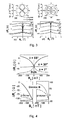
- a ferromagnetic element 1 of a magnetoresistive device in accordance with the present invention is shown.
- the ferromagnetic element 1 is assumed to have homogenously distributed magnetization, although this need not necessarily be the case.
- the ferromagnetic element 1 exhibits magnetic anisotropy defining a magnetic easy axis 2. Magnetic anisotropy may arise as a result of, inter alia , the shape of the element and/or crystal structure.
- the element 1 may be elongate and so the magnetic easy axis 2 may be aligned along a longitudinal axis.
- Magnetisation 3 of the element 1 is aligned along a magnetic easy axis 2.
- An external magnetic field 5 may optionally be applied to support precessional switching and, depending on orientation, to stabilize re-orientation of the magnetisation 3.
- the external magnetic field 5 may be applied globally to an array of ferromagnetic elements (of which the ferromagnetic element 1 is one).
- the external magnetic field 5 may be fixed along the hard axis to facilitate or assist the precessional switching, for example using a permanent magnet.
- the external magnetic field 5 is aligned anti-parallel to the initial magnetization along the easy axis 2 to stabilize re-orientation of the magnetisation 3.
- the external magnetic field 5 need not be aligned along the easy axis 2 and may be orientated at other angles including a hard axis which, for the arrangement shown in Figure 1 , is arranged perpendicular to the easy axis 2.
- the external magnetic field 5 may be variable and may be generated by passing a current through a conductive track (not shown).
- an electric field pulse 7 may be applied, for example perpendicularly to the plane of the layer, to change magnetic anisotropy in the ferromagnetic element 1 temporarily and trigger precessional reorientation of the magnetization 3.
- the magnetization 3 shown as M
- the direction of the effective magnetic field 6 here designated as parallel to positive x-direction.
- more than one gate may be used.
- An electric field pulse 7 is then applied, which causes magnetic anisotropy to change and, thus, the magnetization 3 to be rotated and to begin precessing around the modified effective field.
- the anisotropy field 2 changes causing the effective magnetic field 6 to rotate, i.e. B ⁇ eff + V 0 ⁇ B ⁇ eff V c , and the magnetization 3 starts damped precession around the axis of effective magnetic field 6, i.e. around B eff ( V C ).
- the electric field 7 can be switched off.
- the magnetisation 3 then begins to stabilize (anti-parallel) along the easy axis 2.
- Magnetisation reversal may be understood by considering orientation-dependent energy of magnetization 3.
- the easy axis 2 along the x-axis corresponds to two energy minima divided by a potential barrier.
- the height of the barrier corresponds to the energy increase if the magnetization 3 is aligned along the hard axis.
- Magnetization reversal i.e. reorientation of magnetization by 180°
- TMR tunnelling magnetoresistance
- GMR gigantic magnetoresistance
- magnetization reversal can be achieved without using an assist magnetic field.
- Rotation of easy axis can also be achieved by changing the carrier density in a strained configuration.
- magnetic anisotropy variation can behave in an opposite way.
- magnetic anisotropy in a location in which the element is compressively strained, magnetic anisotropy may be orientated perpendicularly to the plane and in a location in which the element is in tensile strain, the magnetic anisotropy is orientated in plane
- magnetisation reversal is not necessary, in other words magnetisation need not be re-orientated by 180°.
- magnetization reorientation of 90° can be achieved in an element exhibiting cubic magnetic anisotropy, if the easy axis rotates by an angle less than or equal to 22.5° with a longer pulse length (e.g. a half precession pulse) or at larger angles up to 90° for a shorter pulse lengths (e.g. a quarter precession pulse). This can occur in such as we have observed in Ga 1-x Mn x As having very small strain variations resulting from changes in lattice constant of the order of ⁇ 0.01%.
- anisotropic magnetoresistance effects such as anisotropic magnetoresistance (AMR), tunnelling anisotropic magnetoresistance (TAMR) or Coulomb blockade anisotropic magnetoresistance (CBAMR) can be used to read out the magnetization orientation.
- AMR anisotropic magnetoresistance
- TAMR tunnelling anisotropic magnetoresistance
- CBAMR Coulomb blockade anisotropic magnetoresistance
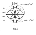
- Figures 2a and 2b illustrate a device 8 in which magnetocrystalline anisotropies are tuned and controlled using strain relaxation arising from lithographically-defined trenches 9.
- the magnetocrystalline anisotropies are induced by spin-orbit coupling.
- a van der Pauw device 10 is defined in the wafer 11 adjacent to the device 8.
- the device 8 is in the form of a Hall bar having a channel 11 which is 'L'-shaped in plan view and which includes first and second arms 11 1 , 11 2 orthogonally aligned along the [110] and [1 1 0] directions.
- the arms have a (transverse) width, w, of 1 ⁇ m and a (longitudinal) length, 1, of 20 ⁇ m.
- the device 8 is formed in a wafer having a layer structure 12 comprising a Ga 0.95 Mn 0.05 As epitaxially-grown layer 13 (or "epilayer) having a thickness of 25 nm grown along the [001] crystal axis on a GaAs substrate 14.
- the channel 11 is defined using electron beam lithography and reactive ion-beam etching.
- the trenches 9 have a (transverse) width, W, of 200 nm and a depth, d, of 70 nm.
- FIG. 3a to 3d electrical characteristics for another device (not shown) having an identical configuration to the device 8 and for the device 8 are shown.
- the other device (not shown) and the device 8 differ in the dimensions of the Hall bars.
- the arms (not shown) are 4 ⁇ m wide and 80 ⁇ m long.
- the arms 11 1 , 11 2 are 1 ⁇ m wide and 20 ⁇ m long.
- These devices 8 exhibit in-plane magnetocrystalline anisotropy and have a saturation magnetisation, M s , of about 50 mT. This arises due to the effect of strain relaxation rather than shape anisotropy.
- shape anisotropy fields for the devices 8 are less than 1 mT, which is one order of magnitude lower than the magnetocrystalline anisotropy fields.
- the easy axes are not defined by shape anisotropy, but rather than magnetocrystalline anisotropy.
- a Curie temperature (T c ) of 100 °K is estimated using Arrot plots of anomalous Hall data.
- a hole density of 5 ⁇ 10 20 cm -3 is estimated from high-field Hall measurements.
- compressive strain in the Ga 0.95 Mn 0.05 As epilayer 13 grown on the GaAs substrate 15 produces a strong magnetocrystalline anisotropy which forces magnetization vector to align parallel with the plane of the magnetic epilayer 13.
- Magnetization orientations in the individual microbar devices 8 are locally monitored by measuring longitudinal and transverse components of the anisotropic magnetoresistance (AMR) for in-plane rotating magnetic field (not shown).
- AMR anisotropic magnetoresistance
- ⁇ L,T ⁇ L,T - ⁇ L,T where ⁇ L,T is the average over all angles.
- Figures 3c and 3d show magnetoresistance plots for external magnetic field sweeps in which a field angle, ⁇ , measured from the [1 1 0] axis, is constant.
- magnetoresistance is strongly dependent at the values of ⁇ and is attributed to magnetization rotations.
- the magnetoresistance becomes purely isotropic, i.e. the differences between resistances for different angles ⁇ become independent of the magnitude of the external field.
- This property and the much smaller magnitude of the isotropic magnetoresistance compared to the low-field anisotropic magnetoresistance enables the high-field measurements shown in Figures 3a and 3b to be used to determine a one-to-one correspondence between a change in the low-field resistance and a change in magnetization orientation.
- the 45° phase shift between the longitudinal and transverse AMR traces shown in Figures 3a and 3b can be used to determine a change in the magnetization angle if both resistance components are measured simultaneously.
- a magnetization angle 30° corresponds to an easy-axis, while 7° and 55° are significantly harder.
- 7° is an easy axes in the [1 1 0]-bar and 55° is an easy-axis in the [110]-bar.
- Table 1 below lists easy axes found in the other device (not shown) labelled 'A', the device 8 labelled 'B' and in bulk material, i.e. in the van der Pauw device 10: Table 1 Sample Bulk A [1 1 0] A [110] B [1 1 0] B[110] Easy axis angle ⁇ 30° ⁇ 15° ⁇ 36° +7°, -8° +55°, -63°
- Bulk material has cubic anisotropy arising from the underlying zincblende structure, plus an additional uniaxial [1 1 0] anisotropy arising from being an (Ga,Mn)As epilayer 13. This results in two easy axes tilted by 15 ⁇ from the [100]and [010] cube edges towards the [1 1 0] direction.
- the easy axes are rotated inwardly from the angles occupied in the bulk material towards the arms 11 1 , 11 2 .
- the degree of rotation increases as the width of the arms 11 1 , 11 2 decreases.
- the local changes in the magnetocrystalline anisotropy may be understood in the following way.
- Ga 0.95 Mn 0.05 As epilayers 13 grown on GaAs substrate 15 are compressively strained in the (001) plane with the typical value of the strain parameter: f ⁇ a GaMnAs - a GaAs a GaAs where a GaAs and a GaMnAs are the lattice parameters of cubic, fully-relaxed GaAs and (Ga,Mn)As, respectively.
- f ⁇ a GaMnAs - a GaAs a GaAs where a GaAs and a GaMnAs are the lattice parameters of cubic, fully-relaxed GaAs and (Ga,Mn)As, respectively.
- the lattice can relax in a transverse direction and the corresponding extension can be roughly estimated as ft / w ⁇ 0.01, where t is the thickness of the (Ga,Mn)As film, in this case 25 nm, and w is the bar width.
- the strength of the lattice relaxation in the microbars can be obtained using numerical elastic theory simulations for the realistic sample geometry.
- GaAs values of the elastic constants are considered for the whole wafer including the Ga 0.95 Mn 0.05 As epilayer 13.
- Figure 5a shows the strain component along the growth-direction [001]-axis with respect to the lattice parameter of a fully relaxed cubic GaAs, namely: e 001 ⁇ a 001 - a GaAs / a GaAs
- Figure 5 illustrates growth-induced lattice matching strain. Because of in-plane compression of the (Ga,Mn)As lattice, the elastic medium reacts by expanding the lattice parameter in the growth direction, as compared to a GaAs , i.e. e [001] / f > 1.
- the lattice can relax only in a direction perpendicular to the microbar orientation.
- the corresponding strain component calculated again with respect to the GaAs, is plotted in Figure 5b over the entire cross-section of device 11 and in Figures 5c and 5d along various cross sections through the [001]-[110] plane. While in the centre of the bar the in-plane relaxation is relatively weak, i.e. the lattice parameter remains similar to that of the GaAs substrate 15, the lattice is strongly relaxed near the edges of the bar 11. Averaged over the entire cross-section of the (Ga,Mn)As bar, relative in-plane lattice relaxation is found to be several hundredths of a per cent, i.e.
- Figure 6a illustrates easy-axes orientations in the [1 1 0]- and [110]-bars of the other 'L'-shaped device 15 and the L'-shaped device 8. Arrows 16 indicate the direction and strength of the patterning induced lattice relaxation.
- Lattice deformations breaking the [1 1 0]-[110] symmetry of the microscopic magnetocrystalline energy profile are illustrated by the diamond-like unit cells extended along [110] axis for the [110]-bar (bottom diamond) and along the [110]axis for the [110]-bar (right diamond).
- the devices just described use the mutual strain relaxation induced by micro-patterning of stripes from GaMnAs with in-plane magnetic anisotropy grown under compressive strain.
- wires which are patterned from tensile strained GaMnAs with perpendicular magnetic anisotropy relax by reducing their lattice constant.
- micro-patterning weakens the perpendicular magnetic anisotropy compared to the tensile strained GaMnAs bulk layer.
- Ferromagnetic metals also exhibit a sensitive dependence of the magnetocrystalline anisotropy on local strain. Any distortion of the equilibrium lattice changes the local anisotropy. In ultrathin films, strain is induced by the growth on a surface. Therefore, similar to GaMnAs, ultrathin layers of cobalt (Co), or iron (Fe) epitaxially grown on a GaAs [001] substrate exhibit both cubic magnetic anisotropy of the bulk, as well as a uniaxial contribution stemming from the interface.
- Co cobalt
- Fe iron
- First and second arrows 17, 18 indicate orientation of the easy axis for the first and second carrier densities respectively.
- magnetoresistance devices will be described in which application of an electric field pulse causes a change in charge carrier density in a ferromagnetic region which in turn causes a change in magnetic anisotropy which causes the magnetisation to begin precession.
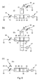
- first and second magnetoresistive devices 21 1 , 21 2 are shown.
- the second devices 21 2 are variants of the first device 21 1 .
- Each device 21 1 , 21 2 includes a ferromagnetic region 22 (herein also referred to as a ferromagnetic "island”) which is under strain.
- the ferromagnetic region 22 comprises a ferromagnetic semiconductor, such as (Ga,Mn)As.
- a different ferromagnetic semiconductor may be used.
- the orientation of magnetisation of the ferromagnetic region 22 can be changed or helped to change by applying a short electric field pulse using a gate 23 capacitively coupled to the ferromagnetic region 22. Applying the electric field pulse causes a change in charge carrier density in the ferromagnetic region 22 which in turn causes a change in magnetic anisotropy which causes the magnetisation to begin precession.
- the ferromagnetic region 22 may be sufficiently small that it exhibits charging effects at a given operating temperature, such as at 4.2 °K.
- the ferromagnetic region 22 may have dimensions (layer thickness and lateral diameter) of the order of 1 or 10 nm. However, the ferromagnetic region 22 may be larger, for example having dimensions of the order of 100 nm, 1 ⁇ m or higher.
- the ferromagnetic island 22 is disposed between first and second leads 24, 25, and is weakly coupled to the leads 24, 25 by respective tunnel barriers 26, 27. In some embodiments, there may be more than one island of ferromagnetic material, for example arranged in chain.
- Reorientation of magnetisation is triggered using a pulse generator 28 which applies a voltage pulse 29 to the gate 23.
- Direction of orientation can be measured in different ways.
- orientation of magnetisation can be determined by measuring tunnelling anisotropic magnetoresistance (TAMR) using voltage source 30 and current detector 31. If the first and/or second lead 24, 25 is ferromagnetic, then the orientation of magnetisation can be determined by measuring tunnelling magnetoresistance (TMR) using voltage source 30 and current detector 31. In either case, the measurement involves applying a voltage so as to drive a current and measuring current.
- TAMR tunnelling anisotropic magnetoresistance
- TMR tunnelling magnetoresistance
- orientation of magnetisation can be determined using by measuring TMR using the voltage source 30 and the current detector 31. However, the bias is applied across and current is measured between the first lead 24 and a third lead 32 which is connected to a pinned ferromagnetic region 33 which is separated from the ferromagnetic island 22 by a tunnel barrier 34. It will be appreciated that a different measurement configuration can be used.
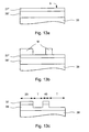
- the first device 21 1 is shown in more detail.
- the first device 21 1 has an elongate conductive channel 36 with the gate 23 arranged to the side of the channel 36, i.e. in a side gate configuration.
- the channel 36 and side gate 23 are formed in a patterned layer 37 of (Ga,Mn)As by trench-isolation.
- a layer 38 of AlAs electrically isolates the channel 36 and the side gate 23 from a GaAs substrate 39.
- the channel 36 includes a constriction 40 disposed between wider portions which provide the leads 24, 25 to the constriction 40.
- the (Ga,Mn)As layer 37 comprises 2% Mn, i.e. Ga 0.98 Mn 0.02 As, and has a thickness of 5 nm, although the effective thickness may be about 3 nm due to surface oxidation.
- the constriction 40 is 30 nm wide and 30 nm long.
- the channel 36 is 2 ⁇ m wide.
- the channel 36 and the gate 23 are separated by about 30 nm.
- potential fluctuations arising from disorder create at least one conductive island 22 and at least a pair of tunnel barriers 26, 27 which weakly couple the island 22 to leads 24, 25 and/or adjacent islands 22.
- Figure 10a is a greyscale plot of channel conductance against gate voltage and in-plane parallel-to-current magnetic field.
- a dashed line 41 highlights critical reorientation field, B C , which depends on gate bias.
- an effective disk diameter of about 10 nm can be estimated using the experimentally-found value of charging energy.
- about 40 Manganese acceptors are present on the island 22.
- About sixteen Coulomb oscillations are observed if V G is varied from -1V to +1V corresponding to a reduction of about 40% in carrier density.
- the second device 21 2 is a variant of the first device 21 1 .
- the devices 21 2 may be formed growing a layer of AlAs 38' on a GaAs substrate 39 followed by a layer of (Ga,Mn)As (not shown), patterning the (Ga,Mn)As to form a underlying electrode structure 42 comprising the pinned layer 32 and the third electrode 33 as a single piece, then growing a further layer of AlAs 43 and a further layer of (Ga,Mn)As over the patterned substrate and patterning the further layer of (Ga,Mn)As to form the channel 37' and gate 23.
- An overlying electrode structure can be used instead of an underlying electrode structure.
- the AlAs layer and (Ga,Mn)As layer forming the electrode may be grown after the channel and gate has been formed and patterned to form the electrode structure comprising the pinned layer and the third electrode.
- a thin gate dielectric, such as Si x N y , and a ferromagnetic material, such as Co may be deposited and patterned using lift-off or dry etching.
- the devices 21 1, 21 2 can exhibit four states M 1 , M 2 , M 3 , M 4 .
- the devices 21 1, 21 2 can exhibit fewer states, for example just two states which may be anti-parallel, or more states, for example six states by taking advantage of in-plane bi-axial anisotropy and perpendicular uni-axial anisotropy.
- the devices 21 1 , 21 2 can exhibit, for example, four states M 1 , M 2 , M 3 , M 4 , depending on whether, for example, the source and/or drain region is ferromagnetic, all states may be distinguishable or, alternatively, some states may be indistinguishable.
- plot of magnetisation 44 shown in Figure 12 does not represent energy of magnetisation, but merely represents different states. In some embodiments, they may represent angle dependencies 0°, 90°, 180°, 270°.
- a voltage pulse 29 is applied to the gate 23.
- the pulse 29 has duration, t 180 , which is half the period of precession, t prescess .
- t precess is about1 ns.
- the value of t precess may lie typically in the range of 100 ps to 10 ns (for B a 100 mT to 1 mT).
- is of the order of 1 or 10 V.
- an external magnetic field may be applied to help stabilise magnetisation or to facilitate precession.
- the external magnetic field may be provided by a permanent magnet (not shown) or by a conductive track (not shown) and preferably has a magnitude which is about the same order but smaller than the anisotropy field, for example of the order of 1 to 100 mT.
- an external magnetic field and/or spin transfer torque current may be used to write a particular state (as opposed to toggle between states) by orientating the magnetisation 44 in a particular direction.
- this is referred to as "direct writing”.
- re-orientation of the magnetisation may be achieved by applying the electric field pulse and simultaneously or shortly afterwards applying a spin transfer torque (STT) current pulse.
- STT spin transfer torque
- a bias pulse 45 is applied between the source 24 and drain 25 of the device 21 1 , 21 2 and the current 31, i, is measured.
- the magnitude of the current depends on the tunnelling anisotropic magnetoresistance (TAMR) and/or the tunnelling magnetoresistance (TMR) of the device which in turn depends on the orientation of magnetisation 44 of the ferromagnetic region 22 which represents '0' and '1' states.
- TAMR tunnelling anisotropic magnetoresistance
- TMR tunnelling magnetoresistance
- orientation of more than two states can be determined by measuring anisotropic magnetoresistance effects such as AMR, TAMR and CBAMR or by measuring a transverse Hall voltage between lead 32 and a reference (e.g. ground) arising from the anomalous Hall effect for states along a perpendicular-to plane magnetic easy axis.
- anisotropic magnetoresistance effects such as AMR, TAMR and CBAMR
- a transverse Hall voltage between lead 32 and a reference e.g. ground
- the device 21 1 is fabricated from an ultra-thin (5nm) Ga 0.98 Mn 0.02 As epilayer 37" grown along the [001] crystal axis on a AlAs 38" buffer layer on a GaAs substrate 39 by low-temperature molecular beam epitaxy (LT-MBE) and reference is made to " High-quality GaMnAs films grown with arsenic dimers" by R. P. Campion, K. W. Edmonds, L. X. Zhao, K. Y. Wang, C. T. Foxon, B. L. Gallagher and C. R. Staddon, Journal of Crystal Growth, volume 247, p 42 (2003 ).
- LT-MBE low-temperature molecular beam epitaxy
- Hall bar 14 is defined using electron-beam lithography using a poly-methyl-methacrylate (PMMA) resist developed using ultrasound in a methyl isobutyl ketone/isopropanol 1:3 mixture at 25 °C.
- PMMA poly-methyl-methacrylate
- Thermally-evaporated, high-electron-contrast Cr/Au registration marks (not shown) having thicknesses of 20 nm and 60 nm respectively are patterned by lift-off using 1 ⁇ m-thick resist (not shown) and ⁇ 250 nm electron-beam diameter. A 30 s dip in 10% HCl solution is used prior to evaporation to assist adhesion of metal without unduly damaging the GaMnAs.
- a ⁇ 200 nm-thick layer of resist (not shown) is applied to the surface S of the Ga 0.98 Mn 0.02 As epilayer 37.
- the finest features are defined using an electron-beam (not shown) having a ⁇ 15 nm beam diameter and ⁇ 5 pA current, with on-chip focusing at adjacent registration marks.
- Less-critical areas are defined in the same resist by a ⁇ 250 nm beam at ⁇ 1 nA.
- the high-resolution regions are arranged to be as small as possible to minimise write time and pattern drift.
- the resist is developed to leave a patterned resist layer M as an etch mask.
- RIE reactive-ion etching
- devices are arranged in a Hall-bar layout aligned along [110] direction, with a 2 ⁇ m-wide channel and three pairs of Hall sensor terminals of 500 nm width at 10 ⁇ m intervals either side of the constriction.
- Hall-bar layout aligned along [110] direction, with a 2 ⁇ m-wide channel and three pairs of Hall sensor terminals of 500 nm width at 10 ⁇ m intervals either side of the constriction.
- Hall sensor terminals 500 nm width at 10 ⁇ m intervals either side of the constriction.
- other arrangements can be used.
- the fabrication process hereinbefore described is modified to fabricate the second devices 21 2 .
- a different initial layer structure is used having a thicker GaMnAs layer, e.g. 25 nm thick.
- the layer structure is patterned using electron beam lithography and RIE to form an underlying electrode structure 44 ( Figure 11a ).
- another AlAs layer (having a thickness of 3nm) and a layer of GaMnAs are grown by LT-MBE as described above.
- the structure is patterned to define the channel in a similar way to the first device 21 1 .
- the underlying electrode structure 44 ( Figure 11a ) may be patterned using ion-beam milling immediately after growth of the initial layer structure, then the additional layers grown without breaking vacuum.
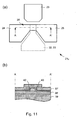
- the third device 21 3 is a two-terminal device having a ferromagnetic region 22 disposed between first and second leads 24, 25 and is weakly coupled to one of the leads 24 by a tunnel barrier 26 and to the other lead 25 by a tunable barrier 35 provided by a region of depletion formed by the semiconducting ferromagnetic region 22 and the lead 25.
- the ferromagnetic region 22 comprises a p-type semiconductor, e.g. Ga(Mn,As) and the lead 25 compirises an n-type semiconductor, e.g. Si doped GaAs, and so the tunable barrier 35 is a reversed-biases p-n junction.
- the lead may be metallic and so the tunable barrier 35 may be a Schottky barrier.
- the device 21 3 comprises a pillar 47 upstanding from a substrate 48.
- the pillar 47 includes a layer 25 of GaAs doped to a concentration of the order of 1-10 ⁇ 10 18 cm -3 and having an (unetched) thickness of 200 nm, a layer 22 of p-type Ga 0.98 Mn 0.02 As having a thickness of about 5 nm, a layer 26 of AlAs having a thickness of 25 nm and a layer of Au having a thickness of about 10 nm.
- the device is fabricated from a layer structure (not shown) grown on an GaAs substrate (not shown) comprising, in order a 200 nm thick layer of n-type GaAs (not shown), a 5 nm thick layer of Ga 0.98 Mn 0.02 As and a 25 nm thick layer of AlAs.
- the Ga 0.98 Mn 0.02 As is grown by low-temperature molecular beam epitaxy (LT-MBE).
- Electron beam lithography and thermal evaporation are used to define a pad of gold (Au) having a thickness of the order of 10 nm on the surface of the layer structure (not shown) and SiCl 4 /Ar RIE is used to define the pillar 47.
- the pillar may be planarised using, for example polyimide, and depositing a gold contact pad.
- a non-magnetic ohmic contact is used to contact the substrate.
- the third device 21 3 can exhibit can exhibit four states M 1 , M 2 , M 3 , M 4 .
- the third device 21 3 differs in that the polarity of a voltage pulse 29 determines whether it is a write or read pulse.
- a negative voltage pulse 29 is applied to the lead 24 adjacent to the fixed tunnel barrier relative to the other lead 25 so as to reverse bias the p-n junction 35 and increase the width of the depletion region to increase depletion and vary the carrier density or carrier density distribution in the ferromagnetic region 22 and, thus, induce precession.
- the duration of the pulse can be use to switch between two states or between more than two states, in other words using t 90 and t 180 pulses.
- a positive bias pulse 30 is applied to the lead 24 adjacent to the fixed tunnel barrier relative to the other lead 25 and the magnetization orientation depending current 46, i, is measured.
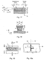
- a magnetoresistive device 51 will now be described in which application of an electric field pulse causes a shift in maximal carrier concentration in an inhomogeneously strained ferromagnetic semiconductor which in turn causes a change in magnetic anisotropy and so initiates precession of magnetisation.
- the device 51 comprises a Hall bar 52 which is generally elongate having width, w, of about 1 ⁇ m and a length, 1, of about 20 ⁇ m.
- the Hall bar 52 has first and second end leads 53, 54 and first, second, third and fourth side leads 55, 56, 57, 58 arranged in pairs on opposite sides of the bar 52.
- the Hall bar 52 is sandwiched between underlying and overlying electrodes 59, 60, hereinafter referred to as "bottom” and “top” electrodes respectively.
- a pulse generator 61 is used to apply a voltage pulse 62 between the top and bottom electrodes 59, 60.
- a current source 63 is used to apply a read current, i read , through the Hall bar 52 between the first and second end leads 53, 54.
- First and second voltage meters 64, 65 measure bias between the first and second leads 55, 56 and between the second and fourth side leads 56, 58 so as to determine longitudinal and transverse anisotropic magnetoresistance (AMR) respectively.
- the bias measured between the second and third side leads 56, 57 can also be used to measure the anomalous Hall effect (AHE) resistance.
- AHE anomalous Hall effect
- the Hall bar 52 is formed on an indium gallium arsenide (In 0.05 Ga 0.95 As) substrate 66 which serves as the bottom electrode 59.
- the Hall bar 52 includes a base barrier layer 67 formed of AlAs overlying the InGaAs substrate 66, an inhomogeneously-strained ferromagnetic layer 68 formed of graded InGaMnAs and a top barrier layer 69 formed of AlAs.
- the top gate electrode 60 is formed of Al.
- the lattice constant within the ferromagnetic layer 68 is controllably varied so as to produce inhomogeneous strain within the layer 68.
- the lattice constant of In 0.03 Ga 0.97 As is larger than the lattice constant for Ga 0.95 Mn 0.05 As so that the subsequent Ga 0.95 Mn 0.05 As grown on In 0.03 Ga 0.97 As is tensile strained.
- Indium is introduced again to form InGaMnAs.
- the Indium concentration is increased until the lattice constant of InGaMnAs becomes larger than the lattice constant of the InGaAs substrate to achieve compressive strain.
- a layer 68 1 ' of Ga 1-x Mn x As is epitaxially grown under tensile strain on top of the AlAs layer 67' which in turn is grown on the In y Ga 1-y As substrate 66'.
- the wider lattice constant of the In y Ga 1-y As substrate 66' is transmitted to the Ga 1-x Mn x As layer 68 1 ' which introduces tensile strain.
- indium is introduced to increase further the lattice constant by thereby forming a quaternary alloy, InGaMnAs.
- the indium concentration [In] increases with increasing distance, d, from the base 71 of the layer 68 1 .
- strain profiles can be used. For example, instead of the strain within the ferromagnetic layer 68 varying from being tensile closer to the substrate to being compressive further away from the substrate, it may change from being compressive to tensile.
- This can be achieved by fabricating the device from a wafer having a gallium arsenide (GaAs) substrate instead of In y Ga 1-y As substrate and introducing phosphorous (P) instead of indium (In) to form a graded layer of gallium manganese phosphide arsenide (Ga 1-x Mn x P z As 1-z ). The lattice constant is reduced as the phosphorous concentration is increased.
- GaAs gallium arsenide
- P phosphorous
- In indium
- strain can also be varied by changing the shape of ferromagnetic layer 68.
- the width of the ferromagnetic layer 68 may be made narrower at the base 71 of the layer 68 having a width w 1 and made wider further away from the base 71 having a width w 2 > w 1 .
- the ferromagnetic layer 68 may be homogenously doped.
- an electric field 72 is generated which shifts charge carriers 73 (here only holes, the majority carriers, are illustrated) and alters charge carrier concentration in a lower, tensile-strained region 74 and in an upper, compressively-strained region 75.
- the pulse draws carriers 73 from the lower, tensile-strained region 74 into the upper, compressively-strained region 75 so as to increase charge carrier density in the upper, compressively-strained region 75.
- Table 2 below identifies orientation of magnetic anisotropy with strain and carrier concentration: Table 2 Tensile Strain Compressive strain High carrier concentration Out of plane In plane Low carrier concentration In plane Out of plane
- Magnetic anisotropy 76 of the magnetic layer 68 changes from being orientated in a first position 77 1 perpendicular to the plane of the layer 68 (i.e. along axis 78) to a second orientation 77 2 orientated along the plane of the layer 68 (e.g. along axis 79).
- the effective anisotropy field B A rotates by 90°. This causes the magnetisation 80 to begin precession and to be re-orientated by 90 degree for a ⁇ /2-pulse.
- Writing and reading cycles are similar to those shown in Figure 12 described earlier. However, during a read cycle, instead of applying a source-drain bias and measuring current, a current is driven through the device and the potential difference developed between leads 55, 56, 57, 58 is measured.
- the device 51 is fabricated using similar techniques to those described earlier to fabricate the first device 21 1 .
- a layer structure is grown in a similar way to that described earlier and is patterned using electron-beam lithography and RIE.
- a fourth magnetoresistive device 81 which does not fall within the scope of claim 1, will now be described in which application of a strain pulse causes a change in magnetic anisotropy and so starts precession of magnetisation.
- the device 81 comprises a stacked layer structure 82 mounted on a piezoelectric layer 83 having first and second contact leads 84, 85.
- First and second contacts 86, 87 are used to provide electrical contacts to the layer structure 82.
- the stacked layer structure 82 has a width, W, of about 1 ⁇ m and a length, L, of about 1 ⁇ m.
- a pulse generator 88 is used to apply a voltage pulse 89 between the piezoelectric contact leads 86, 87.
- a voltage source 90 is used to apply a bias between the contact 86, 87 and a current meter 91 is used to measure the current flowing through the stacked layer structure 82.
- the stacked layer structure 82 is formed on a gallium arsenide (GaAs) substrate 92 which mounted by glue 93 to the piezoelectric stressor 83.
- the piezoelectric stressor is formed from lead-zirconate-titanate (PZT).
- the stacked layer structure 82 includes a bottom contact layer 94 comprising (non-ferromagnetic) n + -GaAs, a ferromagnetic layer 95 having a relatively low coercivity (i.e.
- a "free” layer comprising Ga 0.98 Mn 0.02 As and having a thickness of 5 nm, a tunnel barrier layer 96 comprising aluminium arsenide (AlAs) having a thickness of 25 nm, a ferromagnetic layer 97 having a relatively high coercivity (i.e. a "pinned” layer) comprising Ga 0.98 Mn 0.02 As having a thickness of 50 nm and a top contact layer 98 comprising (non-ferromagnetic) gold.
- AlAs aluminium arsenide
- a ferromagnetic layer 97 having a relatively high coercivity i.e. a "pinned” layer
- Ga 0.98 Mn 0.02 As having a thickness of 50 nm
- a top contact layer 98 comprising (non-ferromagnetic) gold.
- the piezoelectric stressor 83 may be integrally formed with the substrate 92.
- GaAs is piezoelectric along the [110] axis.
- the ferromagnetic layer(s) of the fourth device 81 need not be a semiconductor but may be metallic and may comprise a material, such as ferromagnetic metals like Fe, Ni, Co or metal alloys FePt, CoPt, CoPd or another suitable transition metal/noble metal alloy.
- a stacked layer structure need not be used. Instead, an "in-plane" transport structure, e.g. similar to that shown in Figure 9 , can be used.
- the structure shown in Figure 9 may be mounted on a piezoelectric stressor 83.
- the device 101 comprises a cruciform mesa 102 which defines a channel 103 of ferromagnetic material, which in this case is a delta-doped layer of Ga 0.98 Mn 0.02 As embedded in layer 104 of GaAs, and which is supported by substrate 105.
- First, second, third and fourth contact 106, 107, 108, 109 provide contacts to the distal ends of the channel 103 and a surface top gate 110 is used to control magnetic anisotropy.
- the substrate 104 is mounted on a piezoelectric layer 111 having first and second contacts 112, 113 which are used to generate an electric field within the piezoelectric layer 111 for pre-stressing the ferromagnetic channel 103.
- the arms of the channel 103 each have a width of about 2 ⁇ m and a length of about 20 ⁇ m.
- a first pulse generator 114 is used to apply a voltage pulse 115 between the piezoelectric contact leads 112, 113 for pre-stressing the channel 103.
- a second pulse generator 116 is used to apply a voltage pulse 117 to the surface gate 110 for inducing precession of magnetic anisotropy.
- a voltage source 118 is used to apply a bias 119 between the first and second contact 106, 107 and a current meter 120 is used to measure the current 121 flowing between the third and fourth contacts 108, 109.
- the substrate 104 is mounted to the piezoelectric layer 111 by a layer of glue 122.
- writing and reading of data to the devices is based on treating the device as if it had only two states and, thus, store only one bit of information per device.
- six remnant magnetisation orientations can be accessed using two types of combination of pulses and inverted pulses so as to encode more than 2 bits (i.e. ln 6/ln 2 ⁇ 2.6 corresponding to 6 different states).
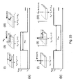
- the ferromagnetic layers 22, 68, 95, 103 exhibit six remnant magnetisation orientations 131, 132, 133, 134, 135, 136.
- precessional switching triggered by fast gate-voltage pulses with different pulse lengths rotate the magnetization vector between the four remnant states 131, 132, 133, 134 along the two biaxial easy axes within the layer plane.
- an adjacent magnetisation orientation 131, 132, 133, 134 can be accessed from another of the first, second, third and fourth magnetisation orientations 131, 132, 133, 134 using a gate pulse 29, 62, 91 which effects a 90° rotation.
- This type of pulse is herein referred to as a "p 90° pulse” or "t 90 pulse”.
- an adjacent magnetisation orientation 131, 132, 133, 134 can be accessed from another of the first, second, third and fourth magnetisation orientations 131, 132, 133, 134 using a gate pulse (not shown) which effects a 270° rotation.
- a gate pulse not shown
- p 270° pulse or "t 270 pulse”.
- the first, second, third and fourth magnetisation orientations 131, 132, 133, 134 can also be accessed from a co-linear orientations 131, 132, 133, 134 using a gate pulse 138 which effects a 180° rotation, hereinafter referred to as a "p 180° pulse” or "t 180 pulse”.
- a gate pulse 138 which effects a 180° rotation
- the first magnetisation orientation 131 can be access the third magnetisation orientation 133 using the p 180° pulse 138.
- Changing between biaxial-in-plane and uniaxial-perpendicular-to-plane anisotropy regimes is achieved by "adiabatic" magnetization reorientation which exploits dissipative damping.
- the magnetization vector M starts precessing around a modified anisotropy field B A (V C ) and dissipative damping causes the magnetization vector to spiral towards modified anisotropy field B A (V C ).
- the magnetization vector M eventually aligns (within thermal fluctuations) along one of the easy axes corresponding to the modified anisotropy.
- the fifth and sixth magnetisation orientations 135, 136 can be accessed by using a gate pulse 141 which effects a 180° rotation.
- the pulse 141 is inverted with respect to the p 180° pulse 108 and is hereinafter referred to as an "inverted p 180° pulse.
- Figures 25b shows that an inverted pulse triggers a 180° reversal in the perpendicular-to-plane anisotropy regime.
- An AHE measurement can distinguish between two uniaxial magnetization states along perpendicular-to-the-plane orientation and measurements of transverse and longitudinal AMR can unambiguously distinguish the 4 biaxial magnetization states within the plane.
- the ferromagnetic layer may have a different thickness, for example between 5 and 20 nm.
- Devices may operate based on electron or hole transfer.
- a capping layer may be used to protect the GaMnAs layer.
- the magnetoresistive device can have a multiple layer structure, such as a magnetic tunnel junction or spin valve.
Landscapes
- Engineering & Computer Science (AREA)
- Computer Hardware Design (AREA)
- Physics & Mathematics (AREA)
- Condensed Matter Physics & Semiconductors (AREA)
- General Physics & Mathematics (AREA)
- Manufacturing & Machinery (AREA)
- Hall/Mr Elements (AREA)
- Mram Or Spin Memory Techniques (AREA)
Claims (12)
- Verfahren zum Betreiben einer magnetoresistiven Vorrichtung mit einer ferromagnetischen Region (22), die so konfiguriert ist, dass sie magnetische Anisotropie aufweist und es zulässt, dass ihre Magnetisierung zwischen wenigstens einer ersten und einer zweiten Orientierung geschaltet wird, und einem kapazitiv mit der ferromagnetischen Region gekoppelten Gatter (23), wobei das Verfahren Folgendes beinhaltet:Anlegen eines elektrischen Feldimpulses (29) an die ferromagnetische Region unter Verwendung des Gatters, um Ladungsträgerverteilung in der ferromagnetischen Region so zu variieren, dass die Ladungsträgerverteilung eine Änderung der Orientierung von magnetischer Anisotropie bewirkt, so dass die Magnetisierung zwischen der ersten und zweiten Orientierung geschaltet wird, wobei der elektrische Feldimpuls eine Dauer t hat, die ein Vielfaches von einem Viertel von etwa tprecess ist:wobei γ die gyromagnetische Konstante γ=gµB/

h (2.2×10¹⁵mA-1s-1) und BA das magnetische Anisotropiefeld der ferromagnetischen Region ist, so dass der elektrische Feldimpuls ein präzessionales Schalten der Magnetisierung zwischen der ersten und zweiten Orientierung auslöst. - Verfahren nach Anspruch 1, das Folgendes beinhaltet:exklusives Anlegen des elektrischen Feldimpulses (29) an die ferromagnetische Region (22), um ein Schalten der Magnetisierung der ferromagnetischen Region zwischen der ersten und zweiten Orientierung zu bewirken.
- Verfahren nach Anspruch 1, das das Arrangieren beinhaltet, dass die Magnetisierung der ferromagnetischen Region zwischen der ersten und zweiten Orientierung ohne Anlegen eines magnetischen Feldimpulses geschaltet wird.
- Verfahren nach Anspruch 1, wobei die Vorrichtung ferner eine neben der ferromagnetischen Region verlaufende Leiterbahn zum Erzeugen eines magnetischen Feldimpulses umfasst, wobei das Verfahren ferner das Anlegen eines magnetischen Feldimpulses an die ferromagnetische Region während des Anlegens des elektrischen Feldimpulses beinhaltet, um die Änderung der Orientierung eines wirksamen Magnetfelds zu verstärken, das ein Anisotropiefeld und ein angelegtes Magnetfeld umfasst, um die Magnetisierung zwischen der ersten und zweiten Orientierung zu schalten.
- Verfahren nach Anspruch 4, das das Anlegen einer vorderen Flanke des elektrischen Feldimpulses vor dem Anlegen einer vorderen Flanke des magnetischen Feldimpulses beinhaltet.
- Verfahren nach einem der vorherigen Ansprüche, wobei die Vorrichtung ferner eine andere ferromagnetische Region mit einer höheren Koerzitivkraft umfasst als die durch eine Tunnelbarrierenschicht davon getrennte ferromagnetische Region, wobei das Verfahren das Anlegen, gleichzeitig oder während die Magnetisierung Präzession erfährt, eines durch ferromagnetische Regionen laufenden Spin-Transfer-Stromimpulses und/oder eines magnetischen Feldimpulses beinhaltet.
- Verfahren nach Anspruch 6, das das Anlegen einer vorderen Flanke des elektrischen Feldimpulses vor dem Anlegen einer vorderen Flanke des Spin-Transfer-Stromimpulses und/oder des magnetischen Feldimpulses beinhaltet.
- Verfahren nach einem der vorherigen Ansprüche, wobei die ferromagnetische Region einen ferromagnetischen Halbleiter mit einer inhomogenen Spannungsverteilung beinhaltet und wobei das Verfahren das Anlegen eines elektrischen Feldimpulses mit einer ausreichenden Größe beinhaltet, um die Verteilung von Ladungsträgern relativ zur inhomogenen Spannungsverteilung zu variieren.
- Verfahren nach Anspruch 8, wobei die inhomogene Spannungsverteilung eine Druckspannungsregion und eine Zugspannungsregion beinhaltet.
- Verfahren nach Anspruch 8 oder 9, wobei der ferromagnetische Halbleiter (Ga, Mn) As beinhaltet.
- Verfahren nach einem der vorherigen Ansprüche, wobei der elektrische Feldimpuls eine Dauer t zwischen 0 und 5 ns hat.
- Vorrichtung, die Folgendes umfasst:eine magnetoresistive Vorrichtung mit einer ferromagnetischen Region, die so konfiguriert ist, dass sie magnetische Anisotropie aufweist und ein Schalten ihrer Magnetisierung zwischen wenigstens einer ersten und einer zweiten Orientierung zulässt, und einem Gatter, das kapazitiv mit der ferromagnetischen Region gekoppelt ist; undeinen Schaltkomplex, der zum Betreiben der Vorrichtung nach einem der vorherigen Ansprüche konfiguriert ist.
Priority Applications (5)
| Application Number | Priority Date | Filing Date | Title |
|---|---|---|---|
| EP07112497.8A EP2015307B8 (de) | 2007-07-13 | 2007-07-13 | Magnetoresistive Vorrichtung |
| US12/050,208 US8138758B2 (en) | 2007-07-13 | 2008-03-18 | Method of controlling a magnetoresistive device using an electric field pulse |
| CN2008101287874A CN101345079B (zh) | 2007-07-13 | 2008-03-19 | 磁电阻器件 |
| KR1020080025611A KR100971843B1 (ko) | 2007-07-13 | 2008-03-19 | 자기저항 디바이스 |
| JP2008170142A JP5121597B2 (ja) | 2007-07-13 | 2008-06-30 | 磁気抵抗素子 |
Applications Claiming Priority (1)
| Application Number | Priority Date | Filing Date | Title |
|---|---|---|---|
| EP07112497.8A EP2015307B8 (de) | 2007-07-13 | 2007-07-13 | Magnetoresistive Vorrichtung |
Publications (3)
| Publication Number | Publication Date |
|---|---|
| EP2015307A1 EP2015307A1 (de) | 2009-01-14 |
| EP2015307B1 true EP2015307B1 (de) | 2013-04-10 |
| EP2015307B8 EP2015307B8 (de) | 2013-05-15 |
Family
ID=39167780
Family Applications (1)
| Application Number | Title | Priority Date | Filing Date |
|---|---|---|---|
| EP07112497.8A Ceased EP2015307B8 (de) | 2007-07-13 | 2007-07-13 | Magnetoresistive Vorrichtung |
Country Status (5)
| Country | Link |
|---|---|
| US (1) | US8138758B2 (de) |
| EP (1) | EP2015307B8 (de) |
| JP (1) | JP5121597B2 (de) |
| KR (1) | KR100971843B1 (de) |
| CN (1) | CN101345079B (de) |
Cited By (14)
| Publication number | Priority date | Publication date | Assignee | Title |
|---|---|---|---|---|
| US9269888B2 (en) | 2014-04-18 | 2016-02-23 | Micron Technology, Inc. | Memory cells, methods of fabrication, and semiconductor devices |
| US9281466B2 (en) | 2014-04-09 | 2016-03-08 | Micron Technology, Inc. | Memory cells, semiconductor structures, semiconductor devices, and methods of fabrication |
| US9349945B2 (en) | 2014-10-16 | 2016-05-24 | Micron Technology, Inc. | Memory cells, semiconductor devices, and methods of fabrication |
| US9356229B2 (en) | 2012-06-19 | 2016-05-31 | Micron Technology, Inc. | Memory cells and methods of fabrication |
| US9368714B2 (en) | 2013-07-01 | 2016-06-14 | Micron Technology, Inc. | Memory cells, methods of operation and fabrication, semiconductor device structures, and memory systems |
| US9379315B2 (en) | 2013-03-12 | 2016-06-28 | Micron Technology, Inc. | Memory cells, methods of fabrication, semiconductor device structures, and memory systems |
| US9406874B2 (en) | 2012-06-19 | 2016-08-02 | Micron Technology, Inc. | Magnetic memory cells and methods of formation |
| US9461242B2 (en) | 2013-09-13 | 2016-10-04 | Micron Technology, Inc. | Magnetic memory cells, methods of fabrication, semiconductor devices, memory systems, and electronic systems |
| US9466787B2 (en) | 2013-07-23 | 2016-10-11 | Micron Technology, Inc. | Memory cells, methods of fabrication, semiconductor device structures, memory systems, and electronic systems |
| US9548444B2 (en) | 2012-03-22 | 2017-01-17 | Micron Technology, Inc. | Magnetic memory cells and methods of formation |
| US9608197B2 (en) | 2013-09-18 | 2017-03-28 | Micron Technology, Inc. | Memory cells, methods of fabrication, and semiconductor devices |
| US9768377B2 (en) | 2014-12-02 | 2017-09-19 | Micron Technology, Inc. | Magnetic cell structures, and methods of fabrication |
| US10439131B2 (en) | 2015-01-15 | 2019-10-08 | Micron Technology, Inc. | Methods of forming semiconductor devices including tunnel barrier materials |
| US10454024B2 (en) | 2014-02-28 | 2019-10-22 | Micron Technology, Inc. | Memory cells, methods of fabrication, and memory devices |
Families Citing this family (30)
| Publication number | Priority date | Publication date | Assignee | Title |
|---|---|---|---|---|
| JP5611594B2 (ja) * | 2007-10-11 | 2014-10-22 | 国立大学法人東北大学 | 不揮発性固体磁気メモリの記録方法及び不揮発性固体磁気メモリ |
| JP2010067304A (ja) * | 2008-09-10 | 2010-03-25 | Hitachi Global Storage Technologies Netherlands Bv | 異常ホール効果を用いた磁気再生素子及び磁気ヘッド |
| FR2937783B1 (fr) * | 2008-10-24 | 2011-06-10 | Inst Nat Polytech Grenoble | Procede et dispositif d'actionnement magnetique |
| EP2209123B1 (de) * | 2009-01-14 | 2011-12-21 | Hitachi, Ltd. | Magnetoresistiver Speicher |
| WO2011006042A1 (en) * | 2009-07-10 | 2011-01-13 | University Of Chicago | System and method for manipulating domain pinning and reversal in ferromagnetic materials |
| JP2011119537A (ja) * | 2009-12-04 | 2011-06-16 | Nec Corp | メモリセル及び磁気ランダムアクセスメモリ |
| US9093163B2 (en) * | 2010-01-14 | 2015-07-28 | Hitachi, Ltd. | Magnetoresistive device |
| US8953366B2 (en) * | 2010-05-11 | 2015-02-10 | University Of Virginia Patent Foundation | Magnetic random access memory device |
| FR2961632B1 (fr) * | 2010-06-18 | 2013-04-19 | Centre Nat Rech Scient | Memoire magnetoelectrique |
| US8374048B2 (en) | 2010-08-11 | 2013-02-12 | Grandis, Inc. | Method and system for providing magnetic tunneling junction elements having a biaxial anisotropy |
| JP5695451B2 (ja) | 2011-03-04 | 2015-04-08 | 株式会社東芝 | 磁気メモリ及び磁気メモリ装置 |
| JP5727836B2 (ja) * | 2011-03-30 | 2015-06-03 | 株式会社東芝 | 磁気記憶素子、磁気記憶装置、磁壁移動方法 |
| WO2012159078A2 (en) * | 2011-05-19 | 2012-11-22 | The Regents Of The University Of California | Voltage-controlled magnetic anisotropy (vcma) switch and magneto-electric memory (meram) |
| EP2541554B1 (de) * | 2011-06-30 | 2015-12-30 | Hitachi, Ltd. | Funktionelle magnetische Vorrichtung |
| KR20140035013A (ko) * | 2012-09-12 | 2014-03-21 | 삼성전자주식회사 | 자기장 생성부 및 이것을 포함하는 반도체 테스트 장치 |
| JP5576449B2 (ja) * | 2012-09-26 | 2014-08-20 | 株式会社東芝 | 不揮発性記憶装置 |
| KR101593665B1 (ko) * | 2012-11-16 | 2016-02-16 | 한국기초과학지원연구원 | 스핀토크형 자기센서 |
| US9042151B2 (en) | 2013-03-15 | 2015-05-26 | International Business Machines Corporation | Racetrack memory with electric-field assisted domain wall injection for low-power write operation |
| US10536281B2 (en) * | 2014-07-30 | 2020-01-14 | University Of South Florida | Magnetic memory physically unclonable functions |
| US9646666B2 (en) * | 2015-02-02 | 2017-05-09 | Globalfoundries Singapore Pte. Ltd. | Voltage controlled spin switches for low power applications |
| US9620562B2 (en) * | 2015-06-02 | 2017-04-11 | Western Digital Technologies, Inc. | Voltage-controlled magnetic anisotropy switching device using an external ferromagnetic biasing film |
| US10674139B2 (en) * | 2015-06-03 | 2020-06-02 | University Of Connecticut | Methods and systems for human action recognition using 3D integral imaging |
| US9825218B2 (en) * | 2015-10-13 | 2017-11-21 | Board Of Regents, The University Of Texas System | Transistor that employs collective magnetic effects thereby providing improved energy efficiency |
| US11996129B2 (en) * | 2016-06-10 | 2024-05-28 | Cornell University | Semiconductor circuits and devices based on low-energy consumption semiconductor structures exhibiting multi-valued magnetoelectric spin hall effect |
| CN109273593B (zh) * | 2018-08-23 | 2021-03-26 | 同济大学 | 利用电流驱动磁矩翻转的单层铁磁材料及其应用 |
| CN109669149B (zh) * | 2019-02-01 | 2021-06-01 | 电子科技大学 | 一种线性各向异性磁电阻传感器及其实现方法 |
| CN110379917B (zh) * | 2019-06-25 | 2021-04-20 | 西安交通大学 | 一种磁多层结构、磁性结器件和磁性随机存储装置及其辅助写入和直接读取方法 |
| US11366182B2 (en) * | 2020-01-24 | 2022-06-21 | Vanguard International Semiconductor Corporation | Magnetoresistive devices and methods for forming the same |
| US20250089577A1 (en) * | 2022-07-12 | 2025-03-13 | Institute of Microelectronics, Chinese Academy of Sciences | Memory cell and method of manufacturing the same, memory, and method of storing information |
| KR20260016865A (ko) | 2024-07-26 | 2026-02-04 | 연세대학교 산학협력단 | 다치레벨로 작동하는 강자성 메모리 장치, 이의 제조 방법, 및 상기 강자성 메모리 장치를 포함하는 시스템 |
Family Cites Families (13)
| Publication number | Priority date | Publication date | Assignee | Title |
|---|---|---|---|---|
| JP4568926B2 (ja) * | 1999-07-14 | 2010-10-27 | ソニー株式会社 | 磁気機能素子及び磁気記録装置 |
| JP2001084756A (ja) * | 1999-09-17 | 2001-03-30 | Sony Corp | 磁化駆動方法、磁気機能素子および磁気装置 |
| JP3932356B2 (ja) * | 2002-07-22 | 2007-06-20 | 国立大学法人東北大学 | 不揮発性固体磁気メモリの記録方法 |
| KR20050053716A (ko) * | 2002-10-03 | 2005-06-08 | 소니 가부시끼 가이샤 | 메모리 소자 및 메모리 장치 |
| JP2005123488A (ja) * | 2003-10-20 | 2005-05-12 | Rikogaku Shinkokai | 磁化反転方法、磁化反転装置、磁気メモリ及び磁気メモリの製造方法 |
| US7282755B2 (en) | 2003-11-14 | 2007-10-16 | Grandis, Inc. | Stress assisted current driven switching for magnetic memory applications |
| EP1548702A1 (de) * | 2003-12-24 | 2005-06-29 | Interuniversitair Microelektronica Centrum Vzw | Verfahren zur superschnellen Steuerung magnetischer Zelle sowie zugehörige Vorrichtungen |
| JP2006165327A (ja) * | 2004-12-08 | 2006-06-22 | Toshiba Corp | 磁気ランダムアクセスメモリ |
| KR100754930B1 (ko) * | 2004-12-22 | 2007-09-03 | 한국과학기술원 | 전압제어 자화반전 기록방식의 mram 소자 및 이를이용한 정보의 기록 및 판독 방법 |
| CN100459149C (zh) * | 2005-03-24 | 2009-02-04 | 株式会社日立制作所 | 导电控制器件 |
| EP1705665B1 (de) * | 2005-03-24 | 2008-04-02 | Hitachi Ltd. | Leitungssteuerungsanordnung |
| JP2006269885A (ja) * | 2005-03-25 | 2006-10-05 | Sony Corp | スピン注入型磁気抵抗効果素子 |
| FR2898414B1 (fr) * | 2006-03-07 | 2008-06-06 | Commissariat Energie Atomique | Composant sensible a un champ magnetique comportant un semi-conducteur magnetique dilue, dispositifs l'incorporant et procede de mise en oeuvre. |
-
2007
- 2007-07-13 EP EP07112497.8A patent/EP2015307B8/de not_active Ceased
-
2008
- 2008-03-18 US US12/050,208 patent/US8138758B2/en not_active Expired - Fee Related
- 2008-03-19 KR KR1020080025611A patent/KR100971843B1/ko not_active Expired - Fee Related
- 2008-03-19 CN CN2008101287874A patent/CN101345079B/zh not_active Expired - Fee Related
- 2008-06-30 JP JP2008170142A patent/JP5121597B2/ja not_active Expired - Fee Related
Cited By (35)
| Publication number | Priority date | Publication date | Assignee | Title |
|---|---|---|---|---|
| US9548444B2 (en) | 2012-03-22 | 2017-01-17 | Micron Technology, Inc. | Magnetic memory cells and methods of formation |
| US9711565B2 (en) | 2012-06-19 | 2017-07-18 | Micron Technology, Inc. | Semiconductor devices comprising magnetic memory cells |
| US10121824B2 (en) | 2012-06-19 | 2018-11-06 | Micron Technology, Inc. | Magnetic structures, semiconductor structures, and semiconductor devices |
| US9356229B2 (en) | 2012-06-19 | 2016-05-31 | Micron Technology, Inc. | Memory cells and methods of fabrication |
| US9406874B2 (en) | 2012-06-19 | 2016-08-02 | Micron Technology, Inc. | Magnetic memory cells and methods of formation |
| US10276781B2 (en) | 2013-03-12 | 2019-04-30 | Micron Technology, Inc. | Magnetoresistive structures, semiconductor devices, and related systems |
| US9379315B2 (en) | 2013-03-12 | 2016-06-28 | Micron Technology, Inc. | Memory cells, methods of fabrication, semiconductor device structures, and memory systems |
| US9972770B2 (en) | 2013-03-12 | 2018-05-15 | Micron Technology, Inc. | Methods of forming memory cells, arrays of magnetic memory cells, and semiconductor devices |
| US9368714B2 (en) | 2013-07-01 | 2016-06-14 | Micron Technology, Inc. | Memory cells, methods of operation and fabrication, semiconductor device structures, and memory systems |
| US10090457B2 (en) | 2013-07-01 | 2018-10-02 | Micron Technology, Inc. | Semiconductor devices with magnetic regions and stressor structures, and methods of operation |
| US9768376B2 (en) | 2013-07-01 | 2017-09-19 | Micron Technology, Inc. | Magnetic memory cells, semiconductor devices, and methods of operation |
| US9466787B2 (en) | 2013-07-23 | 2016-10-11 | Micron Technology, Inc. | Memory cells, methods of fabrication, semiconductor device structures, memory systems, and electronic systems |
| US10515996B2 (en) | 2013-07-23 | 2019-12-24 | Micron Technology, Inc. | Semiconductor devices with seed and magnetic regions and methods of fabrication |
| US9876053B2 (en) | 2013-07-23 | 2018-01-23 | Micron Technology, Inc. | Semiconductor devices comprising magnetic memory cells and methods of fabrication |
| US10290799B2 (en) | 2013-09-13 | 2019-05-14 | Micron Technology, Inc. | Magnetic memory cells and semiconductor devices |
| US10020446B2 (en) | 2013-09-13 | 2018-07-10 | Micron Technology, Inc. | Methods of forming magnetic memory cells and semiconductor devices |
| US9461242B2 (en) | 2013-09-13 | 2016-10-04 | Micron Technology, Inc. | Magnetic memory cells, methods of fabrication, semiconductor devices, memory systems, and electronic systems |
| US9608197B2 (en) | 2013-09-18 | 2017-03-28 | Micron Technology, Inc. | Memory cells, methods of fabrication, and semiconductor devices |
| US10396278B2 (en) | 2013-09-18 | 2019-08-27 | Micron Technology, Inc. | Electronic devices with magnetic and attractor materials and methods of fabrication |
| US9786841B2 (en) | 2013-09-18 | 2017-10-10 | Micron Technology, Inc. | Semiconductor devices with magnetic regions and attracter material and methods of fabrication |
| US10014466B2 (en) | 2013-09-18 | 2018-07-03 | Micron Technology, Inc. | Semiconductor devices with magnetic and attracter materials and methods of fabrication |
| US10454024B2 (en) | 2014-02-28 | 2019-10-22 | Micron Technology, Inc. | Memory cells, methods of fabrication, and memory devices |
| US10026889B2 (en) | 2014-04-09 | 2018-07-17 | Micron Technology, Inc. | Semiconductor structures and devices and methods of forming semiconductor structures and magnetic memory cells |
| US11251363B2 (en) | 2014-04-09 | 2022-02-15 | Micron Technology, Inc. | Methods of forming electronic devices |
| US9281466B2 (en) | 2014-04-09 | 2016-03-08 | Micron Technology, Inc. | Memory cells, semiconductor structures, semiconductor devices, and methods of fabrication |
| US12052929B2 (en) | 2014-04-09 | 2024-07-30 | Micron Technology, Inc. | Methods of forming electronic devices |
| US10505104B2 (en) | 2014-04-09 | 2019-12-10 | Micron Technology, Inc. | Electronic devices including magnetic cell core structures |
| US9269888B2 (en) | 2014-04-18 | 2016-02-23 | Micron Technology, Inc. | Memory cells, methods of fabrication, and semiconductor devices |
| US9543503B2 (en) | 2014-04-18 | 2017-01-10 | Micron Technology, Inc. | Magnetic memory cells and methods of fabrication |
| US9349945B2 (en) | 2014-10-16 | 2016-05-24 | Micron Technology, Inc. | Memory cells, semiconductor devices, and methods of fabrication |
| US10355044B2 (en) | 2014-10-16 | 2019-07-16 | Micron Technology, Inc. | Magnetic memory cells, semiconductor devices, and methods of formation |
| US10347689B2 (en) | 2014-10-16 | 2019-07-09 | Micron Technology, Inc. | Magnetic devices with magnetic and getter regions and methods of formation |
| US10134978B2 (en) | 2014-12-02 | 2018-11-20 | Micron Technology, Inc. | Magnetic cell structures, and methods of fabrication |
| US9768377B2 (en) | 2014-12-02 | 2017-09-19 | Micron Technology, Inc. | Magnetic cell structures, and methods of fabrication |
| US10439131B2 (en) | 2015-01-15 | 2019-10-08 | Micron Technology, Inc. | Methods of forming semiconductor devices including tunnel barrier materials |
Also Published As
| Publication number | Publication date |
|---|---|
| KR20090007201A (ko) | 2009-01-16 |
| CN101345079B (zh) | 2012-09-05 |
| JP5121597B2 (ja) | 2013-01-16 |
| EP2015307A1 (de) | 2009-01-14 |
| JP2009021586A (ja) | 2009-01-29 |
| EP2015307B8 (de) | 2013-05-15 |
| KR100971843B1 (ko) | 2010-07-22 |
| CN101345079A (zh) | 2009-01-14 |
| US20090016098A1 (en) | 2009-01-15 |
| US8138758B2 (en) | 2012-03-20 |
Similar Documents
| Publication | Publication Date | Title |
|---|---|---|
| EP2015307B1 (de) | Magnetoresistive Vorrichtung | |
| US9093163B2 (en) | Magnetoresistive device | |
| EP2209123B1 (de) | Magnetoresistiver Speicher | |
| US9236103B2 (en) | Bipolar spin-transfer switching | |
| US9343658B2 (en) | Magnetic memory bits with perpendicular magnetization switched by current-induced spin-orbit torques | |
| US7813202B2 (en) | Thin-film magnetic device with strong spin polarization perpendicular to the plane of the layers, magnetic tunnel junction and spin valve using such a device | |
| CN103299370B (zh) | 双极性自旋转移切换 | |
| Anguelouch et al. | Two-dimensional magnetic switching of micron-size films in magnetic tunnel junctions | |
| US20110103138A1 (en) | Single-charge tunneling device | |
| Dao et al. | Chiral domain wall injector driven by spin–orbit torques | |
| EP3185245A1 (de) | Antiferromagnetische speichervorrichtung | |
| Gushi | Mn4N thin films for spintronics applications based on current-induced domain wall motion | |
| Gould et al. | Tunneling anisotropic magnetoresistance-based devices | |
| Roschewsky | Spin-Orbit Torques in Ferrimagnets and Topological Insulators | |
| Zhao | Study of Interface Effects on Magnetization Reversal in Magnetic Structures with Perpendicular Magnetic Anisotropy | |
| Chavez | Voltage Control of Magnetism in Nanoscale Artificial Multiferroics | |
| Krishnia | Current-driven domain wall dynamics in coupled ferromagnetic structures | |
| Barra | Magnetic Memory with Antiferromagnets and Multilayers | |
| Schulz | Spin transfer torques in the heavy metal/ferromagnet/oxide hetero-structure Ta/CoFeB/MgO | |
| Steiner | Micromagnetism and Electrical Resistance of Ferromagnetic Electrodes for Spin-Injection Devices | |
| Gould et al. | Novel spintronic devices using local anisotropy engineering in (Ga, Mn) As | |
| Lecture | New-Concept Spintronics Devices |
Legal Events
| Date | Code | Title | Description |
|---|---|---|---|
| PUAI | Public reference made under article 153(3) epc to a published international application that has entered the european phase |
Free format text: ORIGINAL CODE: 0009012 |
|
| AK | Designated contracting states |
Kind code of ref document: A1 Designated state(s): AT BE BG CH CY CZ DE DK EE ES FI FR GB GR HU IE IS IT LI LT LU LV MC MT NL PL PT RO SE SI SK TR |
|
| AX | Request for extension of the european patent |
Extension state: AL BA HR MK RS |
|
| 17P | Request for examination filed |
Effective date: 20090216 |
|
| 17Q | First examination report despatched |
Effective date: 20090323 |
|
| AKX | Designation fees paid |
Designated state(s): DE FR GB |
|
| GRAJ | Information related to disapproval of communication of intention to grant by the applicant or resumption of examination proceedings by the epo deleted |
Free format text: ORIGINAL CODE: EPIDOSDIGR1 |
|
| GRAP | Despatch of communication of intention to grant a patent |
Free format text: ORIGINAL CODE: EPIDOSNIGR1 |
|
| GRAP | Despatch of communication of intention to grant a patent |
Free format text: ORIGINAL CODE: EPIDOSNIGR1 |
|
| GRAS | Grant fee paid |
Free format text: ORIGINAL CODE: EPIDOSNIGR3 |
|
| GRAA | (expected) grant |
Free format text: ORIGINAL CODE: 0009210 |
|
| AK | Designated contracting states |
Kind code of ref document: B1 Designated state(s): DE FR GB |
|
| REG | Reference to a national code |
Ref country code: GB Ref legal event code: FG4D |
|
| RAP2 | Party data changed (patent owner data changed or rights of a patent transferred) |
Owner name: CENTRE NATIONAL DE LA RECHERCHE SCIENTIFIQUE Owner name: UNIVERSITE PARIS SUD XI Owner name: HITACHI LTD. |
|
| REG | Reference to a national code |
Ref country code: DE Ref legal event code: R096 Ref document number: 602007029608 Country of ref document: DE Effective date: 20130613 |
|
| PLBE | No opposition filed within time limit |
Free format text: ORIGINAL CODE: 0009261 |
|
| STAA | Information on the status of an ep patent application or granted ep patent |
Free format text: STATUS: NO OPPOSITION FILED WITHIN TIME LIMIT |
|
| 26N | No opposition filed |
Effective date: 20140113 |
|
| REG | Reference to a national code |
Ref country code: DE Ref legal event code: R097 Ref document number: 602007029608 Country of ref document: DE Effective date: 20140113 |
|
| REG | Reference to a national code |
Ref country code: FR Ref legal event code: PLFP Year of fee payment: 10 |
|
| REG | Reference to a national code |
Ref country code: FR Ref legal event code: PLFP Year of fee payment: 11 |
|
| PGFP | Annual fee paid to national office [announced via postgrant information from national office to epo] |
Ref country code: FR Payment date: 20170613 Year of fee payment: 11 |
|
| PGFP | Annual fee paid to national office [announced via postgrant information from national office to epo] |
Ref country code: DE Payment date: 20170705 Year of fee payment: 11 |
|
| REG | Reference to a national code |
Ref country code: DE Ref legal event code: R119 Ref document number: 602007029608 Country of ref document: DE |
|
| PG25 | Lapsed in a contracting state [announced via postgrant information from national office to epo] |
Ref country code: FR Free format text: LAPSE BECAUSE OF NON-PAYMENT OF DUE FEES Effective date: 20180731 Ref country code: DE Free format text: LAPSE BECAUSE OF NON-PAYMENT OF DUE FEES Effective date: 20190201 |
|
| PGFP | Annual fee paid to national office [announced via postgrant information from national office to epo] |
Ref country code: GB Payment date: 20210616 Year of fee payment: 15 |
|
| GBPC | Gb: european patent ceased through non-payment of renewal fee |
Effective date: 20220713 |
|
| PG25 | Lapsed in a contracting state [announced via postgrant information from national office to epo] |
Ref country code: GB Free format text: LAPSE BECAUSE OF NON-PAYMENT OF DUE FEES Effective date: 20220713 |