EP2015449A1 - Conditionnement pour résonateur piézoélectrique - Google Patents
Conditionnement pour résonateur piézoélectrique Download PDFInfo
- Publication number
- EP2015449A1 EP2015449A1 EP07112477A EP07112477A EP2015449A1 EP 2015449 A1 EP2015449 A1 EP 2015449A1 EP 07112477 A EP07112477 A EP 07112477A EP 07112477 A EP07112477 A EP 07112477A EP 2015449 A1 EP2015449 A1 EP 2015449A1
- Authority
- EP
- European Patent Office
- Prior art keywords
- silicon
- main part
- cover
- case
- eutectic
- Prior art date
- Legal status (The legal status is an assumption and is not a legal conclusion. Google has not performed a legal analysis and makes no representation as to the accuracy of the status listed.)
- Withdrawn
Links
- 238000004806 packaging method and process Methods 0.000 title description 7
- 239000010703 silicon Substances 0.000 claims abstract description 58
- 229910052710 silicon Inorganic materials 0.000 claims abstract description 56
- XUIMIQQOPSSXEZ-UHFFFAOYSA-N Silicon Chemical compound [Si] XUIMIQQOPSSXEZ-UHFFFAOYSA-N 0.000 claims description 57
- 238000000034 method Methods 0.000 claims description 34
- 230000005496 eutectics Effects 0.000 claims description 22
- 238000004519 manufacturing process Methods 0.000 claims description 22
- 235000012431 wafers Nutrition 0.000 claims description 20
- 239000002184 metal Substances 0.000 claims description 13
- 229910052751 metal Inorganic materials 0.000 claims description 13
- 238000000576 coating method Methods 0.000 claims description 12
- 238000009792 diffusion process Methods 0.000 claims description 11
- 238000005530 etching Methods 0.000 claims description 10
- 239000011248 coating agent Substances 0.000 claims description 9
- 238000000708 deep reactive-ion etching Methods 0.000 claims description 9
- 238000007789 sealing Methods 0.000 claims description 7
- 239000000758 substrate Substances 0.000 claims description 7
- 238000005520 cutting process Methods 0.000 claims description 3
- 229910001020 Au alloy Inorganic materials 0.000 claims description 2
- 229910000676 Si alloy Inorganic materials 0.000 claims description 2
- 239000010931 gold Substances 0.000 description 18
- 229910052737 gold Inorganic materials 0.000 description 18
- PCHJSUWPFVWCPO-UHFFFAOYSA-N gold Chemical compound [Au] PCHJSUWPFVWCPO-UHFFFAOYSA-N 0.000 description 17
- 238000002955 isolation Methods 0.000 description 7
- 238000005516 engineering process Methods 0.000 description 4
- 229910015365 Au—Si Inorganic materials 0.000 description 3
- 239000000919 ceramic Substances 0.000 description 3
- 239000000463 material Substances 0.000 description 3
- OFLYIWITHZJFLS-UHFFFAOYSA-N [Si].[Au] Chemical compound [Si].[Au] OFLYIWITHZJFLS-UHFFFAOYSA-N 0.000 description 2
- 239000010453 quartz Substances 0.000 description 2
- VYPSYNLAJGMNEJ-UHFFFAOYSA-N silicon dioxide Inorganic materials O=[Si]=O VYPSYNLAJGMNEJ-UHFFFAOYSA-N 0.000 description 2
- 230000006978 adaptation Effects 0.000 description 1
- 239000003989 dielectric material Substances 0.000 description 1
- 230000002349 favourable effect Effects 0.000 description 1
- 150000002343 gold Chemical class 0.000 description 1
- 238000009413 insulation Methods 0.000 description 1
- 238000012986 modification Methods 0.000 description 1
- 230000004048 modification Effects 0.000 description 1
- 238000005457 optimization Methods 0.000 description 1
- 238000003825 pressing Methods 0.000 description 1
- 239000004065 semiconductor Substances 0.000 description 1
- 238000005476 soldering Methods 0.000 description 1
Images


Classifications
-
- H—ELECTRICITY
- H03—ELECTRONIC CIRCUITRY
- H03H—IMPEDANCE NETWORKS, e.g. RESONANT CIRCUITS; RESONATORS
- H03H9/00—Networks comprising electromechanical or electro-acoustic elements; Electromechanical resonators
- H03H9/02—Details
- H03H9/05—Holders or supports
- H03H9/10—Mounting in enclosures
- H03H9/1007—Mounting in enclosures for bulk acoustic wave [BAW] devices
- H03H9/1014—Mounting in enclosures for bulk acoustic wave [BAW] devices the enclosure being defined by a frame built on a substrate and a cap, the frame having no mechanical contact with the BAW device
-
- H—ELECTRICITY
- H03—ELECTRONIC CIRCUITRY
- H03H—IMPEDANCE NETWORKS, e.g. RESONANT CIRCUITS; RESONATORS
- H03H9/00—Networks comprising electromechanical or electro-acoustic elements; Electromechanical resonators
- H03H9/15—Constructional features of resonators consisting of piezoelectric or electrostrictive material
- H03H9/21—Crystal tuning forks
Definitions
- the present invention concerns packaging for piezoelectric resonators and more particularly for resonators of small dimensions which are most often used for making frequency generators in particular for portable electronic equipment, in numerous fields such as horology, information technology, telecommunications and the medical field.
- Such packaging for quartz or piezoelectric resonators of small dimensions are of two different kinds in the prior art.
- a first kind of packaging concerns metal cases, which are not always available in SMD (Surface Mounted Device) version, and whose minimal size is limited by technology.
- a second kind of packaging concerns ceramics cases, which are SMD, but whose size is limited by the technology of production as well as the tolerances of manufacturing.
- the overall size of the packaging will be either too large or too close to the resonator edges with greater risks of losses due to the tolerances of manufacturing.
- a ceramic package 2 presents an external length size of at least 2mm and external width size of at least 1,2mm. Since the thickness of the package walls 3 are about 0,2mm, the cavity 4 inside has therefore a length size of 1,6mm and a width size of about 0,8mm.
- the main goal of the present invention is to overcome the aforecited drawbacks by providing a package which combines both advantages, namely better dimensional tolerances, coming from manufacturing technology, and the possibility of directly using material of the cover or lid to make a sealing withstanding appreciably higher final assembly temperature.
- a package for receiving a piezoelectric resonator including a main part with a bottom and sides, in which said resonator shall be mounted and a cover fixed to said main part closing said case, wherein the main part and the cover are both made of silicon.
- the silicon main part is manufactured by using a photolithographic process and preferably etched by Deep Reactive Ion Etching.
- a heat sealing is directly done between the cover and the main part by an adequate eutectic of a metal and silicon, said adequate eutectic being preferably an alloy of gold and silicon.
- an adequate eutectic of a metal and silicon said adequate eutectic being preferably an alloy of gold and silicon.
- an anti-diffusion layer is coated under this gold layer. This anti-diffusion layer avoids diffusion of the eutectic within the silicon forming the main part or the lid.
- the invention concerns a component comprising a package according to the first aspect and a piezoelectric resonator mounted in this package.
- the invention concerns an assembly of two silicon wafers comprising a first wafer in which is manufactured a predetermined number of hollowed main parts for receiving piezoelectric resonators, each hollowed main part including a bottom and sides, in which a resonator shall be mounted, and a second wafer forming a cover for each hollowed main part, wherein the main parts and the covers form closed packages.
- a first wafer in which is manufactured a predetermined number of hollowed main parts for receiving piezoelectric resonators, each hollowed main part including a bottom and sides, in which a resonator shall be mounted
- a second wafer forming a cover for each hollowed main part, wherein the main parts and the covers form closed packages.
- the invention concerns a method for manufacturing a package for a piezoelectric resonator, comprising the steps of (i) forming in a silicon substrate a main part including a bottom and sides by a photolithographic process and silicon etching, (ii) coating portions of the main part with metal-plated electrodes, (iii) forming in another silicon substrate a cover, (iv) assembling said main part and said cover with an adequate eutectic of a metal and silicon.
- the etching process used is Deep Reactive Ion Etching.
- the method further comprises the step of mounting a piezoelectric resonator in contact with the metal-plated electrodes prior to assembly the cover with the main part.
- the method further comprises the step of coating an anti-diffusion layer on the sides of the main part or lid below said eutectic.
- the invention concerns a method for manufacturing packages including piezoelectric resonator mounted inside, comprising the steps of (i) forming in a first silicon wafer a predetermined number of hollowed main parts including a bottom and sides by a photolithographic process and silicon etching; (ii) coating portions of the main parts with metal-plated electrodes; (iii) mounting a piezoelectric resonator in each hollowed main parts in contact with the metal-plated electrodes; (iv) forming in another silicon wafer, a cover for each hollowed main part; (v) assembling said predetermined number of hollowed main parts and said cover with an adequate eutectic of a metal and silicon; (vi) cutting adequately said first and second assembled silicon wafers within sides of the main parts to form said predetermined number of packages including a piezoelectric resonator mounted inside.
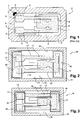
- FIG 2 is a top and cut view of an opened package 10 according to a first embodiment of the invention.
- the package comprises a piezoelectric resonator 11 mounted in a case 12.
- the piezoelectric resonator 11 shown in Figure 2 is a tuning fork resonator having a central arm forming a linking base with the case 12. Nevertheless, it is obviously understood that any other kind of traditional resonators, e.g. tuning fork without a central arm, is also adapted to be mounted within the case 12 which dimensions are adequately modified.
- the case 12 includes a main part with a bottom 13 and sides 14, forming a cavity 15 in which the resonator 11 is mounted and a cover (not shown on this view) fixed to the main part and closing the case.
- the present case 12 is remarkable in that both the main part and the cover are made of silicon.
- thickness of the sides walls are manufactured with high accuracy by using a photolithographic process and silicon etching, so that either the inside cavity 15 is bigger or the overall size of the case (cf. Figure 3 ) can be reduced for a same resonator.
- the etching process used is Deep Reactive Ion Etching (DRIE).
- Figure 3 it shows a top and cut view of an opened package 10 according to another embodiment of the invention similar to the one presented in Figure 2 . Same numerical references have been kept for similar elements.
- the resonator 11 size remains the same.
- inner faces 16 of the sides 14 can be manufactured so as to be really close to the resonator edges 17, so that the overall size of the case 12 is greatly reduced with less risk of short-circuits between electrodes as occurred in the prior art.
- Figure 4 is a top view of the main part of the case without resonator according to the embodiment already illustrated in Figure 2 .
- the main part 20 of case 12 includes a bottom 13 and sides 14 forming a cavity (see figure 5 ) in which the resonator shall be mounted.
- a cover (not shown on this view) is fixed to the main part for closing the case.
- the cavity is coated with conduction deposits 21, such as gold deposits.
- special isolation structures 22 are arranged through the bottom 13.
- isolation structures are made with dielectrics which share the silicon bottom in at least two different potentials, one being set inside the dielectric isolation structure and the other being set around the dielectric isolation structure. Further with such isolation structure 22, there is no more need to pass through a corner of the case to make connections with the outside.
- the upper faces of the sides 14 forming the periphery of the case is coated with a specific proportion of a metal in order to form an eutectic of metal and silicon between the case and the cover to be fixed upon the case.
- the coated layer is a gold layer as well as the conduction deposit inside the case.
- the material used for the main part and the cover both being made of silicon, directly participates as a part of the gold-silicon eutectic (Au-Si) used for sealing the main part with the cover forming the case.
- the gold layer can also be placed on the lid wafer (i.e. cover), and in that case the sides 14 forming the periphery of the case are not coated.
- FIG. 5 it is a cut view of the case 12 represented in Figure 4 along the A-A axis.
- the main part 20 includes a bottom 13 and sides 14 forming the cavity 15.
- the gold deposits 21 connected to the outside via isolated silicon portions 23 obtained by the isolation structures 22 allow simple contacts with the resonator electrodes.
- a bump 27 is advantageously provided with the bottom 13 in order to insure the necessary resonator elevation within the cavity to let it vibrates correctly. This can be easily done when the bump 27 is also made of silicon and can therefore be manufacture at the same time as the sides of the case.
- Another variant is to provide a gold bump, or a gold stud bump on the flat bottom of the case.
- an anti-diffusion layer 24 is advantageously coated on the sides of the main part 20 below the gold layer 25 coated on the upper faces of the sides 14 forming the periphery of the case. This is done in order to avoid massive needs of gold to form the silicon-gold eutectic with the adequate ratio need for sealing. Then the eutectic is obtained only through the gold layer 25 and the cover 26 shown in dotted lines. Conversely, if the anti-diffusion layer and the gold layer are deposited on the silicon lid 26, then the eutectic Au-Si is obtained only through the gold layer and the main part.
- Figures 6a-6f are the steps of a serial manufacturing process of packages including piezoelectric resonators mounted inside cases according to a preferred embodiment of the invention.
- Figure 6a shows two silicon wafers needed as the basic material for the process.
- Figure 6b shows the step of forming in a first silicon wafer a predetermined number of hollowed main parts including a bottom and sides by a photolithographic process, and a silicon etching process, preferably DRIE.
- Figure 6c shows the step of coating portions of the main parts with metal-plated electrodes and coating upper faces of sides, where coatings are preferably made of gold. This step of gold coatings may be achieved either in one step or two steps.
- Figure 6d shows the step of mounting a piezoelectric resonator in each hollowed main parts in contact with the metal-plated electrodes.
- Figure 6e shows the step of forming in another silicon wafer, a cover for each hollowed main part and the step of assembling by sealing said predetermined number of hollowed main parts and said cover with an adequate eutectic of a metal and silicon, obtained with the metal coatings on upper faces of sides.
- Figure 6f shows the step of cutting adequately said first and second silicon wafers within sides of the main parts to form said predetermined number of packages including a piezoelectric resonator mounted inside. Anywhere during the manufacturing process an additional step may consists of isolating the metal plate electrodes by means of isolation structures passing through the first silicon wafer.
- each package comprises a case entirely made of silicon, containing a cavity 15 capable to receive a quartz or piezoelectric resonator with, contact vias towards the outside.
- the present invention also concerns a method for manufacturing a case for a piezoelectric resonator, comprising the steps of forming in a silicon substrate a main part including a bottom and sides by a photolithographic process; coating portions of the main part with metal-plated electrodes; forming in another silicon substrate a cover; assembling said main part and said cover with an adequate eutectic of a metal and silicon.
- This method further comprises the step of mounting a piezoelectric resonator in contact with the metal-plated electrodes prior to assembly the cover with the main part.
- it may be provided an additional step consisting in coating an anti-diffusion layer on the sides of the main part prior to its assembly with the cover, or on the cover.
- the silicon substrate used to manufacture the cavity part can also be a SOI silicon wafer, taking advantage of the mid insulation layer for etch stop function or underlayer for the gold layer.
Landscapes
- Physics & Mathematics (AREA)
- Acoustics & Sound (AREA)
- Piezo-Electric Or Mechanical Vibrators, Or Delay Or Filter Circuits (AREA)
Priority Applications (1)
| Application Number | Priority Date | Filing Date | Title |
|---|---|---|---|
| EP07112477A EP2015449A1 (fr) | 2007-07-13 | 2007-07-13 | Conditionnement pour résonateur piézoélectrique |
Applications Claiming Priority (1)
| Application Number | Priority Date | Filing Date | Title |
|---|---|---|---|
| EP07112477A EP2015449A1 (fr) | 2007-07-13 | 2007-07-13 | Conditionnement pour résonateur piézoélectrique |
Publications (1)
| Publication Number | Publication Date |
|---|---|
| EP2015449A1 true EP2015449A1 (fr) | 2009-01-14 |
Family
ID=38829383
Family Applications (1)
| Application Number | Title | Priority Date | Filing Date |
|---|---|---|---|
| EP07112477A Withdrawn EP2015449A1 (fr) | 2007-07-13 | 2007-07-13 | Conditionnement pour résonateur piézoélectrique |
Country Status (1)
| Country | Link |
|---|---|
| EP (1) | EP2015449A1 (fr) |
Cited By (1)
| Publication number | Priority date | Publication date | Assignee | Title |
|---|---|---|---|---|
| US20140029179A1 (en) * | 2012-07-26 | 2014-01-30 | Seiko Epson Corporation | Resonator element, resonator, oscillator, and electronic apparatus |
Citations (5)
| Publication number | Priority date | Publication date | Assignee | Title |
|---|---|---|---|---|
| US5198716A (en) * | 1991-12-09 | 1993-03-30 | The United States Of America As Represented By The United States Department Of Energy | Micro-machined resonator |
| US5548178A (en) * | 1992-07-08 | 1996-08-20 | Matsushita Electric Industrial Co., Ltd. | Piezoelectric vibrator and manufacturing method thereof |
| US6392144B1 (en) * | 2000-03-01 | 2002-05-21 | Sandia Corporation | Micromechanical die attachment surcharge |
| US20040061207A1 (en) * | 2002-09-30 | 2004-04-01 | Xiaoyi Ding | Hermetically sealed microdevices having a single crystalline silicon getter for maintaning vacuum |
| US20060043540A1 (en) * | 2004-09-01 | 2006-03-02 | Pablo Ferreiro | Silicon package for piezoelectric device |
-
2007
- 2007-07-13 EP EP07112477A patent/EP2015449A1/fr not_active Withdrawn
Patent Citations (5)
| Publication number | Priority date | Publication date | Assignee | Title |
|---|---|---|---|---|
| US5198716A (en) * | 1991-12-09 | 1993-03-30 | The United States Of America As Represented By The United States Department Of Energy | Micro-machined resonator |
| US5548178A (en) * | 1992-07-08 | 1996-08-20 | Matsushita Electric Industrial Co., Ltd. | Piezoelectric vibrator and manufacturing method thereof |
| US6392144B1 (en) * | 2000-03-01 | 2002-05-21 | Sandia Corporation | Micromechanical die attachment surcharge |
| US20040061207A1 (en) * | 2002-09-30 | 2004-04-01 | Xiaoyi Ding | Hermetically sealed microdevices having a single crystalline silicon getter for maintaning vacuum |
| US20060043540A1 (en) * | 2004-09-01 | 2006-03-02 | Pablo Ferreiro | Silicon package for piezoelectric device |
Cited By (2)
| Publication number | Priority date | Publication date | Assignee | Title |
|---|---|---|---|---|
| US20140029179A1 (en) * | 2012-07-26 | 2014-01-30 | Seiko Epson Corporation | Resonator element, resonator, oscillator, and electronic apparatus |
| US9319022B2 (en) * | 2012-07-26 | 2016-04-19 | Seiko Epson Corporation | Resonator element, resonator, oscillator, and electronic apparatus |
Similar Documents
| Publication | Publication Date | Title |
|---|---|---|
| US7026223B2 (en) | Hermetic electric component package | |
| JP4049239B2 (ja) | 表面弾性波素子を含む高周波モジュール部品の製造方法 | |
| US7615833B2 (en) | Film bulk acoustic resonator package and method of fabricating same | |
| CN115485830A (zh) | 包括衬底、集成器件、和具有底切的封装层的封装 | |
| US7034441B2 (en) | Surface mount crystal unit and surface mount crystal oscillator | |
| US8530986B2 (en) | Manufacturing method of electronic device package, electronic device package, and oscillator | |
| TWI480985B (zh) | 一種半導體氣密封裝結構及其製造方法 | |
| JP4938124B2 (ja) | 水晶デバイス | |
| JP5554092B2 (ja) | 電子デバイスパッケージの製造方法 | |
| JP2006147995A (ja) | 可変容量素子及びその製造方法 | |
| WO2007058280A1 (fr) | Plaque de fermeture de composant electronique, plaque de fermeture de composant electronique en plusieurs pieces, dispositif electronique utilisant ladite plaque et procede de fabrication de dispositif electronique | |
| US7351641B2 (en) | Structure and method of forming capped chips | |
| KR20160124323A (ko) | 반도체 소자 패키지 및 그 제조방법 | |
| US12549154B2 (en) | Package comprising an acoustic device and a cap substrate comprising an inductor | |
| US6867060B2 (en) | Wafer-level packaging of electronic devices before singulation | |
| US4722137A (en) | High frequency hermetically sealed package for solid-state components | |
| WO2003003573A1 (fr) | Oscillateur a base de resonateur a quartz forme par l'attache de deux boitiers distincts | |
| JP4010293B2 (ja) | 金属パッケージの製造方法 | |
| CN100446243C (zh) | 堆叠有绝缘腔的芯片 | |
| US20090015107A1 (en) | Packaging for piezoelectric resonator | |
| US6495398B1 (en) | Wafer-scale package for surface acoustic wave circuit and method of manufacturing the same | |
| JP6449620B2 (ja) | 水晶振動子及びその製造方法 | |
| CN106252290A (zh) | 封装外壳及应用该封装外壳的电子元件 | |
| JP2015122413A (ja) | パッケージおよびその製造方法 | |
| JP2017108226A (ja) | トランスデューサ装置及びその製造方法 |
Legal Events
| Date | Code | Title | Description |
|---|---|---|---|
| PUAI | Public reference made under article 153(3) epc to a published international application that has entered the european phase |
Free format text: ORIGINAL CODE: 0009012 |
|
| AK | Designated contracting states |
Kind code of ref document: A1 Designated state(s): AT BE BG CH CY CZ DE DK EE ES FI FR GB GR HU IE IS IT LI LT LU LV MC MT NL PL PT RO SE SI SK TR |
|
| AX | Request for extension of the european patent |
Extension state: AL BA HR MK RS |
|
| AKX | Designation fees paid | ||
| REG | Reference to a national code |
Ref country code: DE Ref legal event code: 8566 |
|
| STAA | Information on the status of an ep patent application or granted ep patent |
Free format text: STATUS: THE APPLICATION IS DEEMED TO BE WITHDRAWN |
|
| 18D | Application deemed to be withdrawn |
Effective date: 20090715 |