EP2016537B1 - Verfahren und einrichtung zum übertragen von daten durch ladungsmodulation - Google Patents
Verfahren und einrichtung zum übertragen von daten durch ladungsmodulation Download PDFInfo
- Publication number
- EP2016537B1 EP2016537B1 EP07734456A EP07734456A EP2016537B1 EP 2016537 B1 EP2016537 B1 EP 2016537B1 EP 07734456 A EP07734456 A EP 07734456A EP 07734456 A EP07734456 A EP 07734456A EP 2016537 B1 EP2016537 B1 EP 2016537B1
- Authority
- EP
- European Patent Office
- Prior art keywords
- voltage
- terminal
- circuit
- load modulation
- antenna circuit
- Prior art date
- Legal status (The legal status is an assumption and is not a legal conclusion. Google has not performed a legal analysis and makes no representation as to the accuracy of the status listed.)
- Not-in-force
Links
Images




Classifications
-
- G—PHYSICS
- G06—COMPUTING OR CALCULATING; COUNTING
- G06K—GRAPHICAL DATA READING; PRESENTATION OF DATA; RECORD CARRIERS; HANDLING RECORD CARRIERS
- G06K19/00—Record carriers for use with machines and with at least a part designed to carry digital markings
- G06K19/06—Record carriers for use with machines and with at least a part designed to carry digital markings characterised by the kind of the digital marking, e.g. shape, nature, code
- G06K19/067—Record carriers with conductive marks, printed circuits or semiconductor circuit elements, e.g. credit or identity cards also with resonating or responding marks without active components
- G06K19/07—Record carriers with conductive marks, printed circuits or semiconductor circuit elements, e.g. credit or identity cards also with resonating or responding marks without active components with integrated circuit chips
- G06K19/0723—Record carriers with conductive marks, printed circuits or semiconductor circuit elements, e.g. credit or identity cards also with resonating or responding marks without active components with integrated circuit chips the record carrier comprising an arrangement for non-contact communication, e.g. wireless communication circuits on transponder cards, non-contact smart cards or RFIDs
-
- G—PHYSICS
- G06—COMPUTING OR CALCULATING; COUNTING
- G06K—GRAPHICAL DATA READING; PRESENTATION OF DATA; RECORD CARRIERS; HANDLING RECORD CARRIERS
- G06K19/00—Record carriers for use with machines and with at least a part designed to carry digital markings
- G06K19/06—Record carriers for use with machines and with at least a part designed to carry digital markings characterised by the kind of the digital marking, e.g. shape, nature, code
- G06K19/067—Record carriers with conductive marks, printed circuits or semiconductor circuit elements, e.g. credit or identity cards also with resonating or responding marks without active components
- G06K19/07—Record carriers with conductive marks, printed circuits or semiconductor circuit elements, e.g. credit or identity cards also with resonating or responding marks without active components with integrated circuit chips
- G06K19/0701—Record carriers with conductive marks, printed circuits or semiconductor circuit elements, e.g. credit or identity cards also with resonating or responding marks without active components with integrated circuit chips at least one of the integrated circuit chips comprising an arrangement for power management
- G06K19/0713—Record carriers with conductive marks, printed circuits or semiconductor circuit elements, e.g. credit or identity cards also with resonating or responding marks without active components with integrated circuit chips at least one of the integrated circuit chips comprising an arrangement for power management the arrangement including a power charge pump
Definitions
- the present invention relates to a method of data transmission by load modulation, and a data transmission device implementing this method.
- the present invention relates in particular to inductive coupling-free data transmission devices, or RFID (Radio Frequency Identification) devices, such as those described by ISO / IEC 14443 and ISO / IEC 15693.
- RFID Radio Frequency Identification
- the present invention relates in particular to non-contact type passive data transmission capable of extracting a power supply voltage from an AC signal provided by their antenna circuit.
- EP-A2-0 899 682 discloses a non-contact data transmission device comprising an antenna circuit providing an AC voltage in the presence of an AC excitation field, and a charge modulation transistor having a control terminal receiving a load modulation signal having at least one low state and one high state, and one conduction terminal receiving the alternating voltage.
- This device also comprises a rectifier circuit for producing, from the AC voltage, a non-boosted DC voltage, a control circuit and a booster circuit for providing a boosted DC voltage greater than a peak value of the AC voltage.
- the control circuit is electrically powered by the boosted DC voltage and provides a load modulation signal which has a high voltage level in the high state. This load modulation signal is applied to the control terminal of the charge modulation transistor.
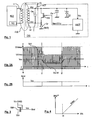
- the figure 1 represents the conventional basic scheme of a passive type DV0 contactless data transmission device for transmitting data by inductive coupling and charge modulation. Such a device will be designated “contactless device” in what follows for the sake of simplification of the language.
- the DV0 device comprises a tuned antenna circuit ACT, a charge modulation transistor SW and a data transmitter circuit DSCT.
- the antenna circuit ACT comprises an antenna coil La and a capacitor Ca in parallel with the antenna coil.
- the charge modulation transistor SW here a MOS transistor, has a first conduction terminal (source) connected to a terminal T1 of the antenna circuit and a second conduction terminal (drain) connected to a terminal T2 of the circuit. antenna.
- a rectifying diode Dr is connected between the terminal T1 and the ground of the device (GND).
- a smoothing capacitor Cs and a Zener diode DZ in parallel are connected between the terminal T2 of the antenna circuit and the ground.
- the non-contact device DV0 is activated by a magnetic field FLD oscillating at a working frequency equal to or close to a tuning frequency of the antenna circuit.
- the magnetic field FLD is for example emitted by a reader RD1, which is equipped for this purpose with an antenna coil Lr and applies thereto an excitation signal oscillating at the working frequency.
- This working frequency is for example 13.56 MHz in a device that complies with one of the ISO standards mentioned above.
- an alternating antenna signal appears in the antenna coil La of the device DV0.
- This antenna signal shows a signal VA1 on terminal T1 of the antenna circuit and a signal VA2 on terminal T2 of the antenna circuit.
- the signal VA1 is a half-wave rectified alternating signal and the signal VA2 is a quasi-continuous signal smoothed by the capacitor. Cs and clipped by the diode DZ, for example in the vicinity of 5 V.
- the non-contact device DV0 is supposed to be here purely passive, the rectified signal VA1 is used as a DC supply voltage Vcc DSCT data transmitter circuit.
- Such a basic non-contact device architecture makes it possible to produce various non-contact electronic portable objects such as contactless smart cards, contactless identification badges, electronic tags, etc.
- the device DSCT applies to the transistor SW a bit charge modulation signal Slm1 which is generated according to the data DTx, these being generally encoded according to a predetermined coding protocol (NRZ, Manchester, BPSK, etc.).
- a predetermined coding protocol NRZ, Manchester, BPSK, etc.
- the signal Slm1 is at "1"
- Vcc voltage
- the transistor SW is then conducting and has a determined series resistance (drain-source resistor RDSon).
- the antenna circuit is thus short-circuited by this resistance, which is generally of the order of a few hundred ohms.
- This short circuit (partial short circuit, the series resistor is not zero) has the effect of modulating the impedance of the antenna circuit and this impedance modulation is reflected by inductive coupling in the antenna signal of the antenna.
- RD1 player can thus, thanks to an appropriate filtering circuit, extract the modulation signal from its own antenna signal and deduce, after demodulation and decoding, the DTx data sent by the device DV0.
- the Figure 2A represents the shape of the signal VA1 when the transistor SW is off, and the shape of the signal VA1 when the transistor SW is on, during a charge modulation period extending between two times t1 and t2.
- the appearance of the supply voltage Vcc is also shown.
- the Figure 2B represents the form of the load modulation signal Slm1, which is at 1 (Vcc, high state) between times t1 and t2 and at 0 (ground, low state) outside the load modulation periods.
- the amplitude of the signal VA1 is maximum and the signal VA1 oscillates between a peak value VA1max and a negative minimum value -Vd equal in absolute value to the threshold voltage Vd of the rectifying diode Dr
- the supply voltage Vcc is also maximum.
- the peak value of the signal VA1 drops substantially and does not exceed a value VA1min, while the supply voltage Vcc also drops.
- This non-contact device structure has the advantage that the depth of the charge modulation, ie the difference between the amplitudes VA1max and VA1 min of the alternating signal VA1, is relatively small and preserves the reception of the electrical energy during the modulation periods. .
- the amplitude of the charge modulation signal detected by the reader RD1 is also a function of the distance between the reader RD1 and the non-contact device DV0: the greater the communication distance, the more the image of the modulation signal of charge mixed with the antenna signal of the reader is low because the inductive coupling is lower. Under these conditions, the communication distance can only be increased by increasing the load modulation depth.
- the variation of the antenna current i in the reader is measured by choosing a determined reader / device distance. The current variation measurement is performed by means of a series resistor giving a voltage V (i). If a minimum voltage variation V (i) min is not reached, the modulation depth is considered insufficient.
- the present invention thus provides a means for increasing the load modulation depth without unjustifiably penalizing the energy reception, essential to supply the supply voltage Vcc to a purely passive contactless device or to provide a voltage auxiliary power supply to a semi-passive contactless device.
- the booster circuit supplies the boosted DC voltage from the AC voltage supplied by the antenna circuit.
- the booster circuit supplies the boosted DC voltage from the unresolved DC voltage.
- the booster circuit comprises at least one stage of a charge pump.
- the charge pump also provides an erase or programming voltage of an electrically erasable and programmable memory.
- the charge pump receives as the pump signal the AC voltage supplied by the antenna circuit.
- the charge modulation transistor is a MOS transistor.
- the antenna circuit comprises an antenna coil which supplies the alternating voltage in the presence of an alternating magnetic field.
- a first terminal of the antenna circuit is connected to a terminal of a rectifying diode whose other terminal receives a reference potential
- a second terminal of the antenna circuit is connected to a terminal of a a smoothing capacitor whose other terminal receives the reference potential
- the AC voltage is present on the first terminal of the antenna circuit
- the second terminal of the antenna circuit has a rectified voltage relative to the reference potential
- the modulation transistor receives the rectified voltage on a first conduction terminal and the alternating voltage on another conduction terminal.
- the invention also relates to an electronic portable object, in particular a smart card or electronic tag, comprising a device according to the invention.
- the boosted DC voltage is produced from the AC voltage supplied by the antenna circuit.
- the boosted DC voltage is produced from the non-boosted DC voltage.
- At least one stage of a charge pump is used to produce the boosted voltage.
- the charge pump is also used to produce an erase or programming voltage of an electrically erasable and programmable memory.
- the AC voltage supplied by the antenna circuit is used as the pump signal of the charge pump.
- a MOS transistor is used as a charge modulation transistor.
- the method comprises the following steps: connecting a first terminal of the antenna circuit to a terminal of a rectifying diode, applying a reference potential to the other terminal of the rectifying diode, connecting a second terminal of the antenna circuit at one terminal of a smoothing capacitor, applying the reference potential to the other terminal of the smoothing capacitor such that the AC voltage appears on the first terminal of the antenna circuit and that a rectified voltage relative to the reference potential appears on the second terminal of the antenna circuit, and apply the rectified voltage to a conduction terminal of the modulation transistor and apply the AC voltage to another conduction terminal of the transistor.
- the present invention provides a means for increasing the charge modulation depth in a non-contact data transmission device of the type shown in FIG. figure 1 , without unjustifiably penalizing the reception of energy, which is essential for supplying the supply voltage Vcc in a passive or semi-passive device (having a supplementary energy source).
- the present invention is based firstly on an analysis of the charge modulation mechanism by the transistor SW configured as shown in FIG. figure 1 .
- the figure 3 is the equivalent diagram of the transistor SW during the load modulation period, when the load modulation signal Slm1 is equal to 1, ie the voltage Vcc ( Fig. 2B ).
- the transistor receives the voltage Vcc on its control terminal, here its gate terminal, and also receives the voltage Vcc (VA2) on a conduction terminal, here its drain terminal, while its other conduction terminal, here its terminal source, receives the half-rectified AC voltage VA1 whose shape is represented in Figure 2A . It thus appears that the transistor has its gate terminal carried at the same potential as its drain terminal.
- the equivalent diagram of the transistor in figure 3 comprises thus a wire connecting the gate terminal and the drain terminal.
- the transistor operates as a diode (saturation regime) and its transconductance function is as shown in FIG. figure 4 , Vds being the drain-source voltage of the transistor, Ids the drain-source current flowing through the transistor, Vt the threshold voltage of the transistor, RDSon its drain-source resistance in the on state.
- VDC - vt > GOES ⁇ 1 is : GOES ⁇ 1 ⁇ VDC - vt
- the transistor SW is on when the AC voltage is lower than Vcc-Vt and is blocked in the opposite case.
- the effective charge modulation zone is therefore reduced and extends between the Vcc-Vt curve represented in FIG. Figure 2A and the right -Vd.
- the load modulation transistor is passing when VA1 is lower than Vcc-Vt, then blocks when VA1 becomes greater than Vcc-Vt, and then again passing when VA1 becomes lower than Vcc-Vt, etc. There is therefore a rapid alternation between the on state and the off state of the transistor.
- the present invention proposes to apply to the gate terminal of the transistor a DC voltage which is greater than the maximum peak voltage VA1max of the AC voltage VA1. . Under these conditions, the transistor is no longer configured as a diode and is continuously passing during the load modulation periods.
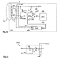
- the figure 5 represents a non-contact data transmission device DV1 according to the invention.
- the device DV1 comprises all the elements of the device DV0 described above, designated by the same references.
- the antenna circuit ACT comprising the coil La and the capacitor Ca
- the rectification diode Dr connected to the terminal T1 of the antenna circuit
- the smoothing capacitor Cs and the clipping diode DZ connected to the terminal are distinguished.
- the device DV1 further comprises a booster circuit BCT and a voltage matching circuit VCT.
- the booster circuit BCT supplies a voltage Vpp1 which is greater than the peak value VA1max that the signal VA1 can exhibit outside the load modulation periods.
- the VCT circuit is powered by the voltage Vpp1 and receives the load modulation signal Slm1 provided by the data transmitter circuit DSCT.
- the high level of the signal Slml substantially corresponds to the voltage Vcc (neglecting the losses in switching elements of the DSCT circuit).
- the VCT circuit converts the signal Slml into a load modulation signal Slm2.
- the VCT circuit may be any known type of voltage adapter, for example a follower amplifier, a gate logic powered by the voltage Vpp1, a trigger or a bistable powered by the voltage Vpp1, ...
- the signal Slm2 is the image of the signal Slml but the high level of this signal is formed by the voltage Vpp1 and not by the voltage Vcc.
- the low level of the signal Slm2 is preferably identical to the low level of the signal Slm1, and here is the potential of the mass (GND).
- the transistor thus operates in linear mode, as shown in FIG. figure 6 , its gate voltage Vpp1 always being greater than its drain-source voltage (Vcc-VA1). The transistor is thus continuously passing when the signal Slm2 is equal to 1 (Vpp1).
- the Figure 7A represents the appearance of the signal VA1 and the voltage Vcc during a load modulation period extending between times t1 and t2, and the Figure 7B represents the form of signal Slm2, equal to Vpp1 between times t1 and t2. Comparing the Figure 7A to the Figure 2A it appears that the alternating signal VA1 oscillates between the threshold voltage of the -Vd diode and a peak voltage VA1min 'which is significantly lower than the peak voltage VA1min of the Figure 2A .
- the load modulation transistor no longer functions as a diode and is equivalent to a resistor.
- the contactless device DV2 represented in figure 8 comprises a charge pump PMP1 for supplying the voltage Vpp1 to the voltage matching circuit VCT.
- the charge pump is powered by the voltage Vcc and receives on inputs IN1, IN2 two anti-phase pumping signals provided by an oscillator OSC.
- the oscillator is preferably of very simple and inexpensive construction. This is for example a ring oscillator, formed by an odd number of cascade inverting gates, the output of the last gate being brought back to the input of the first gate.
- the oscillator is activated by an ON1 signal provided by the DSCT data transmission circuit when the modulation signal Slm2 is to be applied to the modulation switch SW.
- the charge pump PMP1 comprises for example two pumping stages ST1, ST2 in cascade and an output stage comprising a diode D5 and a capacitor C5.
- Stage ST1 comprises two diodes D1, D2 and two capacitors C1, C2.
- Stage ST2 comprises two diodes D3, D4 and two capacitors C3, C4.
- the diode D1 receives the voltage Vcc on its anode and its cathode is connected to the anode of the capacitor C1 and to the anode of the diode D2.
- the cathode of the diode D2 is connected to the anode of the capacitor C2 and to the anode of the diode D3.
- the cathode of the diode D3 is connected to the anode of the capacitor C3 and to the anode of the diode D4.
- the cathode of the diode D4 is connected to the anode of the capacitor C4 and to the anode of the diode D5.
- the cathode of the diode D5 is connected to the anode of the capacitor C5 and supplies the voltage Vpp1.
- the cathode of the capacitor C5 is connected to ground, the cathodes of the capacitors C1, C3 receive the pump signal H1 and the cathodes of the capacitors C2, C4 receive the pump signal H2.
- the voltage Vpp1 is for example 12 to 13 V for a voltage Vcc equal to 5 V and pumping signals having a high level equal to 5 V and a low level equal to 0 V.
- the contactless device DV3 represented in figure 10 comprises a charge pump PMP2 for supplying the voltage Vpp1 to the voltage matching circuit VCT.
- the charge pump is powered by the voltage Vcc and receives on an input IN1 the half-wave alternating signal VA1 taken from the terminal T1 of the antenna circuit, while its other pump input IN2 is connected to ground.
- the charge pump PMP2 is for example made as shown in FIG. figure 11 . It only includes a single ST1 pumping stage identical to that of the PMP1 charge pump.
- the diode D1 receives the voltage Vcc on its anode and its cathode is connected to the anode of the capacitor C1 and to the anode of the diode D2.
- the cathode of the diode D2 is connected to the anode of the capacitor C2 and supplies the voltage Vpp1.
- the cathode of the capacitor C1 receives the alternating signal VA1 and the cathode of the capacitor C2 is connected to ground.
- the voltage Vpp1 is for example 12 to 13 V for a voltage Vcc equal to 5 V and a pump signal VA1 having an amplitude of the order of 8 to 10 V.
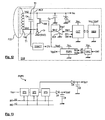
- the non-contact device DV4 represented in figure 12 comprises instead of the circuit DSCT a control circuit CCT microprocessor or wired logic, intended to execute high level commands sent by the reader RD1 (Cf. Fig. 1 ).
- the control circuit CCT is equipped with an electrically erasable and electrically programmable MEM memory (EEPROM) and the commands are, for example, commands for writing or reading the memory, collision control commands, identification commands, etc.
- the device DV4 also comprises a demodulator circuit DEMCT having an input connected to the terminal T1 of the antenna circuit, and an output providing data DTr sent by the reader RD1 by modulation of the amplitude of the magnetic field FLD.
- the DTr data form the aforementioned commands and may include application data to be processed, including data to be written to the memory.
- a charge pump PMP3 is provided to provide a high voltage Vpp2 for erasure and programming of the memory MEM, of the order of 12 V to 15 V.
- the charge pump PMP3 receives on inputs IN1, IN2 signals of pumping H1, H2 provided by an oscillator OSC similar to that described above, activated by a signal ON1 provided by the control circuit CCT.
- the charge pump is also used to supply the voltage Vpp1 of the load modulation signal Slm2.
- the charge pump PMP3 comprises, for example, three pump stages ST1, ST2, ST3 in cascade, a first output stage comprising a diode D5 and a capacitor C5 and a second output stage comprising a diode D6 and a capacitor C6.
- Stages ST1, ST2 and the first output stage are arranged as described in connection with the figure 9 and form the equivalent of the pump PMP1, the cathode of the diode D5 providing the voltage Vpp1.
- Stage ST3 is arranged in cascade with stage ST2 and its output is connected to the anode of diode D6 whose cathode supplies voltage Vpp2 and is connected to the anode of capacitor C6, the cathode of which is connected to the mass.
- the non-contact device DV5 represented on the figure 14 is similar to the device DV4 and differs from it only in that it comprises a charge pump PMP4 receiving as pump signal the AC signal VA1 taken from the terminal T1 of the antenna circuit.
- the signal VA1 is applied to an input IN1 of the charge pump and an input IN2 of the charge pump is connected to ground.
- the charge pump PMP4 comprises two cascade pump stages ST1, ST2 activated here as the pump stage ST1 of the charge pump PMP2 ( Fig. 11 ). So, in the stage ST1, the diode D1 receives the voltage Vcc on its anode and its cathode is connected to the anode of the capacitor C1 and to the anode of the diode D2. The cathode of the diode D2 is connected to the anode of the capacitor C2 and supplies the voltage Vpp1. The cathode of the capacitor C1 receives the alternating signal VA1 and the cathode of the capacitor C2 is connected to ground.
- the anode of the diode D3 is connected to the cathode of the diode D2 of the stage ST1 and receives the voltage Vpp1.
- the cathode of the diode D3 is connected to the anode of the capacitor C3 and to the anode of the diode D4.
- the cathode of the diode D4 is connected to the anode of the capacitor C4 and supplies the voltage Vpp2.
- the cathode of the capacitor C3 receives the alternating signal VA1 and the cathode of the capacitor C2 is connected to ground.
- the charge pumping can be carried out using these two signals as pump signals H1, H2 and by connecting the input of the charge pump to ground.
- the charge modulation transistor may have an intrinsic intrinsic resistance that is very low or at least too low to sufficiently modulate the load of the antenna circuit.
- a load impedance resistance, capacitance Certainly can be arranged in series with the modulation transistor. This load impedance modulates the load of the antenna circuit when the load modulation transistor is conducting, which in this case is used as a simple switch.
- the voltage matching circuit VCT may be an inverter circuit.
- the signal Slm2 is the inverted image of the signal Slm1 and is at the high level, ie the voltage Vpp1, when the signal Slm1 is at the low level.
- the present invention is also susceptible of various applications.
- the DV2, DV3 devices are purely emissive devices and make it possible to carry portable contactless objects of the tag type or of the identifier type, emitting, at certain time intervals, data entered in the DSCT circuit.
- the DV4, DV5 devices are capable of receiving and executing write and read commands from their memory and make it possible to produce various portable objects operating without contact, such as contactless smart cards, contactless electronic badges, contactless electronic tags, etc.
- the various elements constituting the devices DV1 to DV5 are generally integrated on a semiconductor chip, apart from the antenna coil which is generally arranged in or on the support receiving the semiconductor chip, or is disposed on the chip. -Even ("coil on chip").
- the figure 16 represents an electronic tag TG comprising a substrate 10 made of an insulating material (paper, plastic sheet, etc.), an antenna coil 11 and a semiconductor chip 12 incorporating the constituent elements of one of the devices DV1 to DV5 .
- the antenna coil 11 is made by inkjet or by etching a conductive material.
- the lower face of the chip 12 comprises electrical contacts (not shown) which are connected to ends 11-1, 11-2 of the antenna coil.
- the present invention is not limited to inductive coupling circuits and is applicable in a general to any device equipped with an antenna circuit and receiving an induced alternating signal for producing a supply voltage.
- the present invention applies in particular to electrically coupled contactless circuits having an antenna circuit designed to receive a UHF electric field and which modulate the impedance of their antenna circuit, to modulate its reflection coefficient, when data are issued.
Landscapes
- Engineering & Computer Science (AREA)
- Computer Hardware Design (AREA)
- Microelectronics & Electronic Packaging (AREA)
- Physics & Mathematics (AREA)
- General Physics & Mathematics (AREA)
- Theoretical Computer Science (AREA)
- Computer Networks & Wireless Communication (AREA)
- Near-Field Transmission Systems (AREA)
- Selective Calling Equipment (AREA)
- Devices For Checking Fares Or Tickets At Control Points (AREA)
- Radar Systems Or Details Thereof (AREA)
Claims (18)
- Vorrichtung zur Übertragung von Daten ohne Kontakt (DV1, DV2, DV3, DV4, DV5) umfassend- einen Antennenkreis (ACT), der eine Wechselspannung (VA1) in Anwesenheit eines Erregerwechselfeldes (FLD) liefert,- einen Ladungsmodulationstransistor (SW) mit einer Prüfklemme, die ein Ladungsmodulationssignal, das zumindest einen niedrigen Zustand und einen hohen Zustand aufweist, empfängt, und eine Leitungsklemme, die die Wechselspannung (VA1) empfängt,- einen Gleichrichterkreis (Dr, Cs, DZ), um anhand der Wechselspannung (VA1) eine nicht verstärkte Gleichspannung (Vcc) zu erzeugen,- einen Kontrollkreis (DSCT, CCT), der durch die nicht verstärkte Gleichspannung (Vcc) elektrisch versorgt wird, um ein erstes Ladungsmodulationssignal (Slm1), das im hohen Zustand einen nicht verstärkten Spannungspegel (Vcc) aufweist, zu liefern, und- einen Spannungserhöhungskreis (BCT, PMP1-PMP4), um eine verstärkte Gleichspannung (Vpp1), die größer als ein Spitzenwert (VA1max) der Wechselspannung (VA1) ist, zu liefern,dadurch gekennzeichnet, dass sie einen Spannungsanpassungskreis (VCT) zum Umwandeln des ersten Ladungsmodulationssignals (Slml) in ein zweites Ladungsmodulationssignal (Slm2), das im hohen Zustand einen Spannungspegel aufweist, der der verstärkten Gleichspannung (Vpp1) entspricht, umfasst, wobei das zweite Ladungsmodulationssignal an die Prüfklemme des Ladungsmodulationstransistors (SW) angewandt wird.
- Vorrichtung nach Anspruch 1, in der der Spannungserhöhungskreis (BCT, PMP1-PMP4) die verstärkte Gleichspannung (Vpp1) anhand der Wechselspannung (VA1), die vom Antennenkreis (ACT) geliefert wird, liefert.
- Vorrichtung nach Anspruch 1, in der der Spannungserhöhungskreis (BCT, PMP1-PMP4) die verstärkte Gleichspannung (Vpp1) anhand der nicht verstärkten Gleichspannung (Vcc) liefert.
- Vorrichtung nach einem der Ansprüche 2 und 3, in der der Spannungserhöhungskreis zumindest eine Stufe einer Ladungspumpe (PMP1-PMP4) umfasst.
- Vorrichtung nach Anspruch 4, in der die Ladungspumpe (PMP3, PMP4) ebenfalls eine Lösch- oder Programmierspannung (Vpp2) eines elektrisch lösch- und programmierbaren Speichers liefert.
- Vorrichtung nach einem der Ansprüche 4 und 5, in der die Ladungspumpe (PMP2, PMP4) als Pumpsignal die Wechselspannung (VA1), die vom Antennenkreis geliefert wird, empfängt.
- Vorrichtung nach einem der Ansprüche 1 bis 6, in der der Ladungsmodulationstransistor (SW) ein MOS-Transistor ist.
- Vorrichtung nach einem der Ansprüche 1 bis 7, in der der Antennenkreis (ACT) eine Antennenspule (La), die die Wechselspannung (VA1) in Anwesenheit eines magnetisches Wechselfeldes (FLD) liefert, umfasst.
- Vorrichtung nach einem der Ansprüche 1 bis 8, in der:- eine erste Klemme (T1) des Antennenkreises mit einer Klemme von einer Gleichrichterdiode (Dr), von der die andere Klemme ein Bezugspotential (GND) empfängt, verbunden ist,- eine zweite Klemme (T2) des Antennenkreises mit einer Klemme von einem Ladekondensator (Cs), von der die andere Klemme das Bezugspotential empfängt, verbunden ist,- die Wechselspannung (VA1) an der ersten Klemme (T1) des Antennenkreises anwesend ist,- die zweite Klemme (T2) des Antennenkreises eine gleichgerichtete Spannung (AC2, Vcc) im Verhältnis zum Bezugspotential aufweist, und- der Modulationstransistor (SW) die gleichgerichtete Spannung an einer ersten Leitungsklemme (T1) und die Wechselspannung (VA1) an einer anderen Leitungsklemme empfängt.
- Tragbarer elektronischer Gegenstand, insbesondere Chipkarte oder elektronisches Etikett (TG), umfassend eine Vorrichtung nach einem der Ansprüche 1 bis 9.
- Verfahren zur Übertragung von Daten ohne Kontakt durch induktive Kopplung und Ladungsmodulation, umfassend die Schritte, die folgendes beinhalten:- einen Antennenkreis (ACT), der eine Wechselspannung (VA1) in Anwesenheit eines Erregerwechselfeldes (FLD) liefert, vorsehen,- einen Ladungsmodulationstransistor (SW) mit einer Prüfklemme, um ein Ladungsmodulationssignal, das zumindest einen niedrigen Zustand und einen hohen Zustand aufweist, zu empfangen, und mit einer Leitungsklemme, die mit einer Klemme (T1) des Antennenkreises (ACT) verbunden ist und die Wechselspannung (VA1), die vom Antennenkreis geliefert wird, empfängt, vorsehen,- einen Gleichrichterkreis (Dr, Cs, DZ) vorsehen, um anhand der Wechselspannung (VA1) eine nicht verstärkte Gleichspannung (Vcc) zu erzeugen,- einen Kontrollkreis (DSCT, CCT), der durch die nicht verstärkte Gleichspannung (Vcc) elektrisch versorgt wird, um ein erstes Ladungsmodulationssignal (Slml), das im hohen Zustand einen nicht verstärkten Spannungspegel (Vcc) aufweist, zu liefern, vorsehen,- eine verstärkte Gleichspannung (Vpp1), die größer als der Spitzenwert (VA1max) der Wechselspannung (VA1) ist, erzeugen,Wobei das Verfahren dadurch gekennzeichnet ist, dass es die folgenden Schritte umfasst:- das erste Ladungsmodulationssignal (Slm1) in ein zweites Ladungsmodulationssignal (Slm2), das im hohen Zustand einen Spannungspegel aufweist, der der verstärkten Gleichspannung (Vpp1) entspricht, umwandeln, und- das zweite Ladungsmodulationssignal (Slm2) an die Prüfklemme des Ladungsmodulationstransistors (SW) anwenden.
- Verfahren nach Anspruch 11, in dem die verstärkte Gleichspannung (Vpp1) anhand der Wechselspannung (VA1), die vom Antennenkreis geliefert wird, erzeugt wird.
- Verfahren nach Anspruch 12, in dem die verstärkte Gleichspannung (Vpp1) anhand der nicht verstärkten Gleichspannung (Vcc) erzeugt wird.
- Verfahren nach einem der Ansprüche 11 bis 13, in dem zumindest eine Stufe einer Ladungspumpe (PMP1-PMP4) verwendet wird, um die verstärkte Spannung (Vpp1) zu erzeugen.
- Verfahren nach Anspruch 14, in dem die Ladungspumpe (PMP3, PMP4) ebenfalls verwendet wird, um eine Lösch- oder Programmierspannung (Vpp2) eines elektrisch lösch- und programmierbaren Speichers zu erzeugen.
- Verfahren nach einem der Ansprüche 14 und 15, in dem die Wechselspannung (VA1), die vom Antennenkreis (ACT) geliefert wird, als Pumpsignal der Ladungspumpe (PMP2, PMP4) verwendet wird.
- Verfahren nach einem der Ansprüche 11 bis 16, in dem ein MOS-Transistor als Ladungsmodulationstransistor (SW) verwendet wird.
- Verfahren nach einem der Ansprüche 11 bis 17, umfassend die folgenden Schritte:- eine erste Klemme (T1) des Antennenkreises an eine Klemme einer Gleichrichterdiode (Dr) anschließen,- ein Bezugspotential an die andere Klemme der Gleichrichterdiode (Dr) anwenden,- eine zweite Klemme (T2) des Antennenkreises (ACT) an eine Klemme eines Ladekondensators anschließen,- das Bezugspotential an die andere Klemme des Ladekondensators anwenden,
so dass die Wechselspannung (VA1) an der ersten Klemme (T1) des Antennenkreises erscheint, und dass eine gleichgerichtete Spannung im Verhältnis zum Bezugspotential an der zweiten Klemme (T2) des Antennenkreises erscheint, und- die gleichgerichtete Spannung an eine Leitungsklemme des Ladungsmodulationstransistors anwenden und die Wechselspannung (VA1) an eine andere Leitungsklemme des Transistors anwenden.
Applications Claiming Priority (2)
| Application Number | Priority Date | Filing Date | Title |
|---|---|---|---|
| FR0604086A FR2900752B1 (fr) | 2006-05-05 | 2006-05-05 | Procede et dispositif de transmission de donnees par modulation de charge |
| PCT/IB2007/001139 WO2007129187A1 (fr) | 2006-05-05 | 2007-05-02 | Procede et dispositif de transmission de donnees par modulation de charge |
Publications (2)
| Publication Number | Publication Date |
|---|---|
| EP2016537A1 EP2016537A1 (de) | 2009-01-21 |
| EP2016537B1 true EP2016537B1 (de) | 2009-09-23 |
Family
ID=37667652
Family Applications (1)
| Application Number | Title | Priority Date | Filing Date |
|---|---|---|---|
| EP07734456A Not-in-force EP2016537B1 (de) | 2006-05-05 | 2007-05-02 | Verfahren und einrichtung zum übertragen von daten durch ladungsmodulation |
Country Status (8)
| Country | Link |
|---|---|
| US (1) | US8285204B2 (de) |
| EP (1) | EP2016537B1 (de) |
| CN (1) | CN101438302B (de) |
| AT (1) | ATE443902T1 (de) |
| CA (1) | CA2651297C (de) |
| DE (1) | DE602007002561D1 (de) |
| FR (1) | FR2900752B1 (de) |
| WO (1) | WO2007129187A1 (de) |
Families Citing this family (15)
| Publication number | Priority date | Publication date | Assignee | Title |
|---|---|---|---|---|
| TWI361603B (en) * | 2008-04-25 | 2012-04-01 | Univ Nat Taiwan | Signal conversion device, radio frequency tag, and method for operating the same |
| JP6178424B2 (ja) | 2012-11-14 | 2017-08-09 | ヴェクトリアス メディカル テクノロジーズ リミテッド | 埋め込み型静電容量ベース圧力変換器のためのドリフト補償 |
| WO2014170771A1 (en) | 2013-04-18 | 2014-10-23 | Vectorious Medical Technologies Ltd. | Remotely powered sensory implant |
| US10205488B2 (en) | 2013-04-18 | 2019-02-12 | Vectorious Medical Technologies Ltd. | Low-power high-accuracy clock harvesting in inductive coupling systems |
| CN105577896B (zh) * | 2014-10-14 | 2019-08-02 | 国民技术股份有限公司 | 信息互传的方法及系统 |
| WO2016178197A1 (en) | 2015-05-07 | 2016-11-10 | Vectorious Medical Technologies Ltd | Deploying and fixating an implant across an organ wall |
| EP3398237B1 (de) | 2015-12-30 | 2020-12-02 | Vectorious Medical Technologies Ltd. | Leistungseffizientes drucksensorimplantat |
| CN111264034A (zh) * | 2017-10-25 | 2020-06-09 | 日本精机株式会社 | 接收电路和通信装置 |
| DE102017126349A1 (de) | 2017-11-10 | 2019-05-16 | Bundesdruckerei Gmbh | Verfahren zum verknüpfen eines ersten datenblocks mit einem zweiten datenblock, verfahren zum überprüfen der integrität einer blockchain-struktur, vorrichtung und computerprogrammprodukt |
| FR3074940A1 (fr) * | 2017-12-07 | 2019-06-14 | Stmicroelectronics (Rousset) Sas | Detection d'un dispositif nfc |
| KR102603180B1 (ko) * | 2017-12-14 | 2023-11-16 | 삼성전자주식회사 | Nfc 장치의 변조 인덱스 설정 회로, nfc 장치 및 nfc 장치의 동작 방법 |
| CN108534826A (zh) * | 2018-03-26 | 2018-09-14 | 王智华 | 无线通信系统、检测装置及建筑结构 |
| WO2019220232A1 (en) * | 2018-05-17 | 2019-11-21 | Vectorious Medical Technologies Ltd. | Low-power high-accuracy clock harvesting in inductive coupling systems |
| EP3742341B1 (de) | 2019-05-20 | 2022-07-27 | Nxp B.V. | Rfid-transponder und verfahren zum betrieb davon |
| EP3751462B1 (de) | 2019-06-11 | 2022-01-05 | Nxp B.V. | Transponder und entsprechendes betriebsverfahren |
Family Cites Families (10)
| Publication number | Priority date | Publication date | Assignee | Title |
|---|---|---|---|---|
| GB9007791D0 (en) * | 1990-04-06 | 1990-06-06 | Foss Richard C | High voltage boosted wordline supply charge pump and regulator for dram |
| US6054925A (en) * | 1997-08-27 | 2000-04-25 | Data Investments Limited | High impedance transponder with improved backscatter modulator for electronic identification system |
| FR2776865B1 (fr) * | 1998-03-31 | 2000-05-05 | Commissariat Energie Atomique | Dispositif de teletransmission par couplage inductif |
| FR2791493B1 (fr) * | 1999-03-25 | 2001-06-08 | Inside Technologies | Circuit d'emission/reception de donnees par couplage inductif |
| FR2791489B1 (fr) * | 1999-03-25 | 2001-06-08 | Inside Technologies | Procede de modulation de l'amplitude d'un signal d'antenne |
| FR2815490B1 (fr) * | 2000-10-16 | 2006-07-07 | Inside Technologies | Lecteur de circuit integre sans contact |
| DE10151440C1 (de) * | 2001-10-18 | 2003-02-06 | Siemens Ag | Organisches Elektronikbauteil, Verfahren zu seiner Herstellung und seine Verwendung |
| FR2831305B1 (fr) * | 2001-10-23 | 2004-01-30 | Inside Technologies | Circuit integre sans contact comprenant des moyens d'identification automatique de trame |
| US7494066B2 (en) * | 2003-12-19 | 2009-02-24 | Semiconductor Energy Laboratory Co., Ltd. | Semiconductor device |
| FR2888652B1 (fr) * | 2005-07-18 | 2007-10-12 | Oberthur Card Syst Sa | Procede et dispositif de securisation active pour dispositif electronique sans contact |
-
2006
- 2006-05-05 FR FR0604086A patent/FR2900752B1/fr not_active Expired - Fee Related
-
2007
- 2007-05-02 CA CA2651297A patent/CA2651297C/fr active Active
- 2007-05-02 CN CN2007800162199A patent/CN101438302B/zh not_active Expired - Fee Related
- 2007-05-02 WO PCT/IB2007/001139 patent/WO2007129187A1/fr not_active Ceased
- 2007-05-02 EP EP07734456A patent/EP2016537B1/de not_active Not-in-force
- 2007-05-02 AT AT07734456T patent/ATE443902T1/de active
- 2007-05-02 DE DE602007002561T patent/DE602007002561D1/de active Active
- 2007-05-02 US US12/299,391 patent/US8285204B2/en not_active Expired - Fee Related
Also Published As
| Publication number | Publication date |
|---|---|
| CN101438302B (zh) | 2011-06-29 |
| CN101438302A (zh) | 2009-05-20 |
| FR2900752B1 (fr) | 2008-10-10 |
| ATE443902T1 (de) | 2009-10-15 |
| CA2651297A1 (fr) | 2007-11-15 |
| HK1130338A1 (en) | 2009-12-24 |
| WO2007129187A1 (fr) | 2007-11-15 |
| US20090203313A1 (en) | 2009-08-13 |
| FR2900752A1 (fr) | 2007-11-09 |
| CA2651297C (fr) | 2014-11-18 |
| EP2016537A1 (de) | 2009-01-21 |
| DE602007002561D1 (de) | 2009-11-05 |
| US8285204B2 (en) | 2012-10-09 |
Similar Documents
| Publication | Publication Date | Title |
|---|---|---|
| CA2651297C (fr) | Procede et dispositif de transmission de donnees par modulation de charge | |
| US11734540B1 (en) | Rectifier backflow reduction via biasing | |
| US10819319B1 (en) | Level shifter circuit with self-gated transition amplifier | |
| US10713549B1 (en) | RFID tag rectifiers with bias current reuse | |
| US10885417B1 (en) | Impedance-change mitigation in RFID tags | |
| JP5155642B2 (ja) | Idタグ | |
| KR101043835B1 (ko) | 듀얼 안테나를 포함하는 rfid 태그 | |
| US8403233B2 (en) | Semiconductor integrated circuit device and IC card mounting same | |
| US9000835B1 (en) | Hot RF rectifiers for RFID applications | |
| JP4732320B2 (ja) | Rfidタグおよびそれを有するrfidシステム | |
| EP2728822A2 (de) | Demodulationsvorrichtung und Verfahren zum Betrieb davon | |
| FR2891639A1 (fr) | Moyen pour desactiver un dispositif sans contact. | |
| FR2812142A1 (fr) | Transpondeur passif et lecteur pour une identification sans contact de tels transpondeurs | |
| US7671748B2 (en) | Radiofrequency identification device (RFID) affixed to an object to be identified | |
| EP1043679B1 (de) | Leser mit Einrichtung zur Bestimmung des Abstandes zwischen dem Leser und einem Transponder | |
| US8022889B2 (en) | Antenna impedance modulation method | |
| US8140009B2 (en) | Circuit and data carrier with radio frequency interface | |
| US20030160650A1 (en) | Wide dynamic range demodulator for smart cards or contactless tickets | |
| EP1796023B1 (de) | Kontaktloser integrierter Schaltkreis mit einer Energieversorgungsschaltung hohen Wirkungsgrades | |
| JPH11261339A (ja) | 非接触型icカードの変調信号入力回路 | |
| WO2025081128A1 (en) | Rfid tag rectifier with active bias ladders | |
| KR101010146B1 (ko) | 듀얼 안테나를 포함하는 rfid 태그 | |
| HK1130338B (en) | Method and device for transmitting data by charge modulation | |
| WO2016091829A1 (fr) | Procede de communication radiofrequence avec discrimination de lecteur radiofrequence |
Legal Events
| Date | Code | Title | Description |
|---|---|---|---|
| PUAI | Public reference made under article 153(3) epc to a published international application that has entered the european phase |
Free format text: ORIGINAL CODE: 0009012 |
|
| 17P | Request for examination filed |
Effective date: 20081015 |
|
| AK | Designated contracting states |
Kind code of ref document: A1 Designated state(s): AT BE BG CH CY CZ DE DK EE ES FI FR GB GR HU IE IS IT LI LT LU LV MC MT NL PL PT RO SE SI SK TR |
|
| AX | Request for extension of the european patent |
Extension state: AL BA HR MK RS |
|
| GRAP | Despatch of communication of intention to grant a patent |
Free format text: ORIGINAL CODE: EPIDOSNIGR1 |
|
| DAX | Request for extension of the european patent (deleted) | ||
| RBV | Designated contracting states (corrected) |
Designated state(s): AT DE FR GB |
|
| GRAS | Grant fee paid |
Free format text: ORIGINAL CODE: EPIDOSNIGR3 |
|
| GRAA | (expected) grant |
Free format text: ORIGINAL CODE: 0009210 |
|
| AK | Designated contracting states |
Kind code of ref document: B1 Designated state(s): AT DE FR GB |
|
| REG | Reference to a national code |
Ref country code: GB Ref legal event code: FG4D Free format text: NOT ENGLISH |
|
| REF | Corresponds to: |
Ref document number: 602007002561 Country of ref document: DE Date of ref document: 20091105 Kind code of ref document: P |
|
| PLBE | No opposition filed within time limit |
Free format text: ORIGINAL CODE: 0009261 |
|
| STAA | Information on the status of an ep patent application or granted ep patent |
Free format text: STATUS: NO OPPOSITION FILED WITHIN TIME LIMIT |
|
| 26N | No opposition filed |
Effective date: 20100624 |
|
| REG | Reference to a national code |
Ref country code: DE Ref legal event code: R081 Ref document number: 602007002561 Country of ref document: DE Owner name: INSIDE SECURE, FR Free format text: FORMER OWNER: INSIDE CONTACTLESS, AIX EN PROVENCE, FR Effective date: 20131111 |
|
| REG | Reference to a national code |
Ref country code: FR Ref legal event code: CD Owner name: INSIDE SECURE, FR Effective date: 20140129 Ref country code: FR Ref legal event code: CA Effective date: 20140129 |
|
| REG | Reference to a national code |
Ref country code: FR Ref legal event code: PLFP Year of fee payment: 9 |
|
| REG | Reference to a national code |
Ref country code: FR Ref legal event code: CL Name of requester: FRANCE BREVETS , FR Effective date: 20151027 |
|
| REG | Reference to a national code |
Ref country code: FR Ref legal event code: PLFP Year of fee payment: 10 |
|
| REG | Reference to a national code |
Ref country code: AT Ref legal event code: HC Ref document number: 443902 Country of ref document: AT Kind code of ref document: T Owner name: INSIDE SECURE, FR Effective date: 20160601 |
|
| REG | Reference to a national code |
Ref country code: FR Ref legal event code: PLFP Year of fee payment: 11 |
|
| REG | Reference to a national code |
Ref country code: GB Ref legal event code: 732E Free format text: REGISTERED BETWEEN 20170615 AND 20170621 |
|
| REG | Reference to a national code |
Ref country code: FR Ref legal event code: PLFP Year of fee payment: 12 |
|
| REG | Reference to a national code |
Ref country code: DE Ref legal event code: R081 Ref document number: 602007002561 Country of ref document: DE Owner name: VERIMATRIX, FR Free format text: FORMER OWNER: INSIDE SECURE, MEYREUIL, FR |
|
| REG | Reference to a national code |
Ref country code: AT Ref legal event code: HC Ref document number: 443902 Country of ref document: AT Kind code of ref document: T Owner name: VERIMATRIX, FR Effective date: 20200618 |
|
| PGFP | Annual fee paid to national office [announced via postgrant information from national office to epo] |
Ref country code: GB Payment date: 20220519 Year of fee payment: 16 |
|
| PGFP | Annual fee paid to national office [announced via postgrant information from national office to epo] |
Ref country code: AT Payment date: 20220523 Year of fee payment: 16 |
|
| PGFP | Annual fee paid to national office [announced via postgrant information from national office to epo] |
Ref country code: DE Payment date: 20220722 Year of fee payment: 16 |
|
| PGFP | Annual fee paid to national office [announced via postgrant information from national office to epo] |
Ref country code: FR Payment date: 20230525 Year of fee payment: 17 |
|
| REG | Reference to a national code |
Ref country code: DE Ref legal event code: R119 Ref document number: 602007002561 Country of ref document: DE |
|
| REG | Reference to a national code |
Ref country code: AT Ref legal event code: MM01 Ref document number: 443902 Country of ref document: AT Kind code of ref document: T Effective date: 20230502 |
|
| GBPC | Gb: european patent ceased through non-payment of renewal fee |
Effective date: 20230502 |
|
| PG25 | Lapsed in a contracting state [announced via postgrant information from national office to epo] |
Ref country code: AT Free format text: LAPSE BECAUSE OF NON-PAYMENT OF DUE FEES Effective date: 20230502 |
|
| PG25 | Lapsed in a contracting state [announced via postgrant information from national office to epo] |
Ref country code: DE Free format text: LAPSE BECAUSE OF NON-PAYMENT OF DUE FEES Effective date: 20231201 Ref country code: GB Free format text: LAPSE BECAUSE OF NON-PAYMENT OF DUE FEES Effective date: 20230502 |
|
| PG25 | Lapsed in a contracting state [announced via postgrant information from national office to epo] |
Ref country code: FR Free format text: LAPSE BECAUSE OF NON-PAYMENT OF DUE FEES Effective date: 20240531 |