EP2017880A2 - Festkörperzeitmessvorrichtung mit einem Schwebegattertransistor - Google Patents
Festkörperzeitmessvorrichtung mit einem Schwebegattertransistor Download PDFInfo
- Publication number
- EP2017880A2 EP2017880A2 EP08160605A EP08160605A EP2017880A2 EP 2017880 A2 EP2017880 A2 EP 2017880A2 EP 08160605 A EP08160605 A EP 08160605A EP 08160605 A EP08160605 A EP 08160605A EP 2017880 A2 EP2017880 A2 EP 2017880A2
- Authority
- EP
- European Patent Office
- Prior art keywords
- floating gate
- aging device
- gate electrode
- control gate
- element region
- Prior art date
- Legal status (The legal status is an assumption and is not a legal conclusion. Google has not performed a legal analysis and makes no representation as to the accuracy of the status listed.)
- Withdrawn
Links
- 230000032683 aging Effects 0.000 claims abstract description 78
- 238000009792 diffusion process Methods 0.000 claims abstract description 50
- 239000004065 semiconductor Substances 0.000 claims abstract description 44
- 239000000758 substrate Substances 0.000 claims abstract description 36
- 230000008878 coupling Effects 0.000 claims abstract description 30
- 238000010168 coupling process Methods 0.000 claims abstract description 30
- 238000005859 coupling reaction Methods 0.000 claims abstract description 30
- 239000010410 layer Substances 0.000 claims description 82
- 239000000463 material Substances 0.000 claims description 43
- 238000002955 isolation Methods 0.000 claims description 34
- 239000011800 void material Substances 0.000 claims description 25
- 229910021420 polycrystalline silicon Inorganic materials 0.000 claims description 19
- 229920005591 polysilicon Polymers 0.000 claims description 19
- 239000002356 single layer Substances 0.000 claims description 19
- 150000004767 nitrides Chemical class 0.000 claims description 4
- 238000000034 method Methods 0.000 description 6
- 238000002347 injection Methods 0.000 description 3
- 239000007924 injection Substances 0.000 description 3
- 239000011810 insulating material Substances 0.000 description 3
- 230000008859 change Effects 0.000 description 2
- 230000006872 improvement Effects 0.000 description 2
- 238000004519 manufacturing process Methods 0.000 description 2
- 230000002123 temporal effect Effects 0.000 description 2
- 229910052581 Si3N4 Inorganic materials 0.000 description 1
- 230000006870 function Effects 0.000 description 1
- 230000014759 maintenance of location Effects 0.000 description 1
- 230000004048 modification Effects 0.000 description 1
- 238000012986 modification Methods 0.000 description 1
- 230000008569 process Effects 0.000 description 1
- 229910052710 silicon Inorganic materials 0.000 description 1
- 239000010703 silicon Substances 0.000 description 1
- HQVNEWCFYHHQES-UHFFFAOYSA-N silicon nitride Chemical compound N12[Si]34N5[Si]62N3[Si]51N64 HQVNEWCFYHHQES-UHFFFAOYSA-N 0.000 description 1
- 239000007787 solid Substances 0.000 description 1
- 230000005641 tunneling Effects 0.000 description 1
Images


Classifications
-
- G—PHYSICS
- G04—HOROLOGY
- G04F—TIME-INTERVAL MEASURING
- G04F10/00—Apparatus for measuring unknown time intervals by electric means
- G04F10/10—Apparatus for measuring unknown time intervals by electric means by measuring electric or magnetic quantities changing in proportion to time
-
- H—ELECTRICITY
- H10—SEMICONDUCTOR DEVICES; ELECTRIC SOLID-STATE DEVICES NOT OTHERWISE PROVIDED FOR
- H10D—INORGANIC ELECTRIC SEMICONDUCTOR DEVICES
- H10D84/00—Integrated devices formed in or on semiconductor substrates that comprise only semiconducting layers, e.g. on Si wafers or on GaAs-on-Si wafers
- H10D84/01—Manufacture or treatment
- H10D84/02—Manufacture or treatment characterised by using material-based technologies
- H10D84/03—Manufacture or treatment characterised by using material-based technologies using Group IV technology, e.g. silicon technology or silicon-carbide [SiC] technology
- H10D84/038—Manufacture or treatment characterised by using material-based technologies using Group IV technology, e.g. silicon technology or silicon-carbide [SiC] technology using silicon technology, e.g. SiGe
-
- G—PHYSICS
- G11—INFORMATION STORAGE
- G11C—STATIC STORES
- G11C16/00—Erasable programmable read-only memories
- G11C16/02—Erasable programmable read-only memories electrically programmable
- G11C16/04—Erasable programmable read-only memories electrically programmable using variable threshold transistors, e.g. FAMOS
- G11C16/0408—Erasable programmable read-only memories electrically programmable using variable threshold transistors, e.g. FAMOS comprising cells containing floating gate transistors
-
- H—ELECTRICITY
- H10—SEMICONDUCTOR DEVICES; ELECTRIC SOLID-STATE DEVICES NOT OTHERWISE PROVIDED FOR
- H10D—INORGANIC ELECTRIC SEMICONDUCTOR DEVICES
- H10D30/00—Field-effect transistors [FET]
- H10D30/60—Insulated-gate field-effect transistors [IGFET]
- H10D30/68—Floating-gate IGFETs
- H10D30/681—Floating-gate IGFETs having only two programming levels
-
- H—ELECTRICITY
- H10—SEMICONDUCTOR DEVICES; ELECTRIC SOLID-STATE DEVICES NOT OTHERWISE PROVIDED FOR
- H10D—INORGANIC ELECTRIC SEMICONDUCTOR DEVICES
- H10D30/00—Field-effect transistors [FET]
- H10D30/60—Insulated-gate field-effect transistors [IGFET]
- H10D30/68—Floating-gate IGFETs
- H10D30/6891—Floating-gate IGFETs characterised by the shapes, relative sizes or dispositions of the floating gate electrode
-
- H—ELECTRICITY
- H10—SEMICONDUCTOR DEVICES; ELECTRIC SOLID-STATE DEVICES NOT OTHERWISE PROVIDED FOR
- H10D—INORGANIC ELECTRIC SEMICONDUCTOR DEVICES
- H10D84/00—Integrated devices formed in or on semiconductor substrates that comprise only semiconducting layers, e.g. on Si wafers or on GaAs-on-Si wafers
-
- G—PHYSICS
- G11—INFORMATION STORAGE
- G11C—STATIC STORES
- G11C2216/00—Indexing scheme relating to G11C16/00 and subgroups, for features not directly covered by these groups
- G11C2216/02—Structural aspects of erasable programmable read-only memories
- G11C2216/10—Floating gate memory cells with a single polysilicon layer
-
- H—ELECTRICITY
- H10—SEMICONDUCTOR DEVICES; ELECTRIC SOLID-STATE DEVICES NOT OTHERWISE PROVIDED FOR
- H10B—ELECTRONIC MEMORY DEVICES
- H10B41/00—Electrically erasable-and-programmable ROM [EEPROM] devices comprising floating gates
- H10B41/60—Electrically erasable-and-programmable ROM [EEPROM] devices comprising floating gates the control gate being a doped region, e.g. single-poly memory cell
-
- H—ELECTRICITY
- H10—SEMICONDUCTOR DEVICES; ELECTRIC SOLID-STATE DEVICES NOT OTHERWISE PROVIDED FOR
- H10B—ELECTRONIC MEMORY DEVICES
- H10B69/00—Erasable-and-programmable ROM [EPROM] devices not provided for in groups H10B41/00 - H10B63/00, e.g. ultraviolet erasable-and-programmable ROM [UVEPROM] devices
-
- H—ELECTRICITY
- H10—SEMICONDUCTOR DEVICES; ELECTRIC SOLID-STATE DEVICES NOT OTHERWISE PROVIDED FOR
- H10D—INORGANIC ELECTRIC SEMICONDUCTOR DEVICES
- H10D30/00—Field-effect transistors [FET]
- H10D30/01—Manufacture or treatment
- H10D30/021—Manufacture or treatment of FETs having insulated gates [IGFET]
- H10D30/0411—Manufacture or treatment of FETs having insulated gates [IGFET] of FETs having floating gates
-
- H—ELECTRICITY
- H10—SEMICONDUCTOR DEVICES; ELECTRIC SOLID-STATE DEVICES NOT OTHERWISE PROVIDED FOR
- H10D—INORGANIC ELECTRIC SEMICONDUCTOR DEVICES
- H10D64/00—Electrodes of devices having potential barriers
- H10D64/01—Manufacture or treatment
- H10D64/031—Manufacture or treatment of data-storage electrodes
- H10D64/035—Manufacture or treatment of data-storage electrodes comprising conductor-insulator-conductor-insulator-semiconductor structures
Definitions
- the present invention relates to an aging device which is an electronic timer free from a battery.
- an electronic timer free from a battery that is, an aging device in which output is varied as time passes is beginning to be used in the fields of content delivery, credit cards, rental of digital products, rental of digital software, and so on.
- the aging device has a floating gate and operates as an electronic timer for measuring a certain period by using retention characteristics (life) of a charge in the floating gate (for example, see Jpn. Pat. Appln. KOKAI Publication Nos. 2004-172404 and 2005-310824 ).
- the amount of the charge injected into the floating gate and the thickness of a tunnel insulating film are changed, whereby the life of the aging device can be changed.
- stack gate type There are two types of the aging devices: stack gate type and single-layer polysilicon type.
- a basic structure of the stack gate type is the same as the basic structure of a memory cell of a flash memory, it is preferable that the stack gate type is adopted when the aging device is mounted on an IC with a built-in flash memory.
- the aging device is also employed in an IC without a flash memory.
- Jpn. Pat. Appln. KOKAI Publication No. 2007-184321 proposes the single-layer polysilicon type.
- This single-layer polysilicon type is characterized in that a writing/erasing part (second element region) is provided in addition to an aging device part (first element region).
- a floating gate is disposed so as to cross over both the aging device part and the writing/erasing part.
- a coupling capacitance between the floating gate and the first element region is rendered larger than a coupling capacitance between the floating gate and the second element region, whereby the charge is easily injected and ejected between the writing/erasing part (second element region) and the floating gate.
- positive high voltage is applied to an N-type diffusion layer in the first element region, which is the aging device part, in the writing.
- negative high voltage is also preferably applied to the N-type diffusion layer in the second element region as the writing/erasing part, it is difficult to simultaneously apply the positive and negative high voltages to the same semiconductor substrate.
- the positive high voltage is applied to the N-type diffusion layer in the second element region, which is the writing/erasing part, in the erasing.
- the negative high voltage is also preferably applied to the N-type diffusion layer in the first element region as the aging device part, it is difficult to do that for the reason described above.
- An aging device comprises a semiconductor substrate, an element isolation insulating layer formed in a surface region of the semiconductor substrate, a first element region surrounded by the element isolation insulating layer, first and second diffusion layers formed in the first element region, a channel region provided between the first and second diffusion layers, a floating gate formed above the channel region, a control gate electrode provided beside the floating gate with an interval in a lateral direction.
- a coupling capacitance between the floating gate and the control gate electrode is larger than a coupling capacitance between the floating gate and the semiconductor substrate.
- control gate electrodes are arranged at an interval in a lateral direction to a floating gate, and, at the same time, a coupling capacitance between the floating gate and a control gate electrode is rendered larger than a coupling capacitance between the floating gate and a semiconductor substrate.
- the aging device part and a writing/erasing part are not separated from each other, unlike the prior single-layer polysilicon type. Therefore, the device structure is simplified, and, at the same time, writing/erasing is easily controlled. In addition, the entire size of the aging device is reduced.
- the coupling capacitance between the floating gate and the control gate electrode is rendered larger than the coupling capacitance between the floating gate and the semiconductor substrate, whereby, when writing voltage is applied to the control gate electrode, the charge is effectively injected from the semiconductor substrate to the floating gate.
- a voltage is applied to between the semiconductor substrate and the control gate electrode, whereby writing/erasing is performed. Therefore, a positive high voltage (or negative high voltage) is applied to the control gate electrode, and a negative high voltage (or positive high voltage) is applied to the semiconductor substrate, whereby the writing speed can be further increased.
- the single-layer polysilicon type aging device suitable for high-speed writing/erasing can be realized.
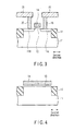
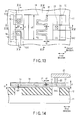
- FIG. 1 shows a plan view of an aging device of the first embodiment.
- FIG. 2 is a cross-sectional view along a line II-II in FIG. 1 .
- FIG. 3 is a cross-sectional view along a line III-III in FIG. 1 .
- FIG. 4 is a cross-sectional view along a line IV-IV in FIG. 1 .
- An element isolation insulating layer 12 with an STI (shallow trench isolation) structure is formed in a semiconductor substrate 11.
- First and second element regions (active areas) AA1 and AA2 are surrounded by the element isolation insulating layer 12 and disposed adjacent to each other in a first direction, for example.
- the width in the first direction of the first element region AA1 is W1.
- Diffusion layers 11A and 11B are formed in the first element region AA1.
- the conductivity type of the diffusion layers 11A and 11B is opposite to the conductivity type of the semiconductor substrate 11. For instance, when the semiconductor substrate 11 is a p-type, the diffusion layers 11A and 11B are an n-type, and, when the semiconductor substrate 11 is the n-type, the diffusion layers 11A and 11B are the p-type.
- a floating gate 14 with a thickness of d is formed above a channel region between the diffusion layers 11A and 11B at an interval t1.
- An area 13 between the first element region AA1 and the floating gate 14 is filled with a material or remains void.
- a control gate electrode 16 is formed above the second element region AA2.
- An area 15 between the second element region AA2 and the control gate electrode 16 is filled with a material or remains void.
- the floating gate 14 is disposed above the first element region AA1 and above the element isolation insulating layer 12 between the first and second element regions AA1 and AA2.
- the width on the first element region AA1 is L1
- the width in the part adjacent to the control gate electrode 16 is L2 (> L1).
- the floating gate 14 and the control gate electrode 16 are adjacent to each other with an interval t2.
- An area 17 between the floating gate 14 and the control gate electrode 16 is filled with a material or remains void.
- a coupling capacitance Cl between the first element region AA1 and the floating gate 14 is ⁇ 1 (L1 ⁇ W1)/t1
- a coupling capacitance C2 between the floating gate 14 and the control gate electrode 16 is ⁇ 2 (L2 ⁇ d)/t2.
- ⁇ 1 represents a dielectric constant of a material or a void in the area 13 between the first element region AA1 and the floating gate 14
- ⁇ 2 represents a dielectric constant of a material or a void in the area 17 between the floating gate 14 and the control gate electrode 16.
- the capacitances C1 and C2 are set to satisfy the expression: C1 ⁇ C2.
- the diffusion layer 11A is connected to a first bit line 19 through a contact plug 18. Meanwhile, the diffusion layer 11B is connected to a second bit line 21 through a contact plug 20.
- the control gate electrode 16 is connected to a word line 23 through a contact plug 22.
- a coupling ratio C2/(C1 + C2) is substantially large.
- a voltage applied to between the substrate 11 and the floating gate 14 is larger when a writing voltage is applied to the control gate electrode 16, and therefore, a writing/erasing efficiency is improved.
- the technique in a flash memory is used for writing (initializing) to the aging device of FIGS. 1 to 4 .
- the voltage of the control gate electrode 16 is set to be a sufficiently higher than the voltage in the channel region, whereby an electron is injected from the channel region into the floating gate 14, using an FN (Fowler-Nordheim) tunneling.
- the aging device measures a temporal change in the amount of the charge accumulated in the floating gate 14, that is, measures it for a certain period using a phenomenon where the voltage of the channel region is changed due to the charge leaking. In other words, the aging device monitors a temporal change (aging) in an electric current (drain current Id) flowing between the first bit line (drain electrode) 19 and the second bit line (source electrode) 21.
- the amount of charge to be injected into the floating gate 14 can be controlled by a verify technique.
- the amount of charge to be injected into the floating gate 14 can be properly controlled by using the verify technique.
- the leakage characteristics are examined before shipment, whereby it is possible to determine conditions of a method of writing (injection of charge) to a control device in accordance with the result of the examination of the leakage characteristics.
- the charge amount to be injected into the floating gate of the control device is changed, whereby the aging devices manufactured in the same line can be provided as the aging devices with different lifes.
- users can set the life of the aging device using the above conditions in accordance with their purpose, and, at the same time, can control difference of each life caused by the variation in manufacturing.
- an end user having purchased a product with the aging device mounted therein can use the product only during the period set by a provider of the product without knowing such a condition. More specifically, even if the end user connects the product to network or disconnects it from an external power supply, the user cannot use the product beyond the period set by the provider.
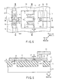
- the second embodiment is a variation of the first embodiment.
- the second embodiment is characterized in that, with regard to a floating gate and a control gate electrode, concavities and convexities are formed in a part where the floating gate and the control gate electrode are faced to each other, whereby the coupling ratio is further improved.
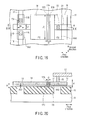
- FIG. 5 shows a plan view of an aging device of the second embodiment.
- FIG. 6 is a cross-sectional view along a line VI-VI in FIG. 5 .
- FIG. 7 is a cross-sectional view along a line VII-VII in FIG. 5 .
- FIG. 8 is a cross-sectional view along a line VIII-VIII in FIG. 5 .
- An element isolation insulating layer 12 with the STI structure is formed in a semiconductor substrate 11.
- First and second element regions (active areas) AA1 and AA2 are surrounded by the element isolation insulating layer 12, and, for example, disposed adjacent to each other in the first direction.
- Diffusion layers 11A and 11B are formed in the first element region AA1.
- the conductivity type of the diffusion layers 11A and 11B is opposite to the conductivity type of the semiconductor substrate 11.
- a floating gate 14 is formed above a channel region between the diffusion layers 11A and 11B.
- An area 13 between the first element region AA1 and the floating gate 14 is filled with a material or remains void.
- a control gate electrode 16 is formed above the second element region AA2.
- An area 15 between the second element region AA2 and the control gate electrode 16 is filled with a material or remains void.
- the floating gate 14 is disposed above the first element region AA1 and above the element isolation insulating layer 12 between the first and second element regions AA1 and AA2.
- the width on the first element region AA1 is L1
- the width in the part adjacent to the control gate electrode 16 is L2 (> L1).
- the floating gate 14 and the control gate electrode 16 are adjacent to each other. Concavities and convexities are formed in a part where the floating gate 14 and the control gate electrode 16 are faced to each other.
- An area 17 between the floating gate 14 and the control gate electrode 16 is filled with a material or remains void.
- ⁇ 1 represents a dielectric constant of a material or a void in the area 13 between the first element region AA1 and the floating gate 14.
- the diffusion layer 11A is connected to a first bit line 19 through a contact plug 18. Meanwhile, the diffusion layer 11B is connected to a second bit line 21 through a contact plug 20.
- the control gate electrode 16 is connected to a word line 23 through a contact plug 22.
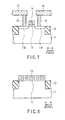
- the third embodiment is a variation of the second embodiment.
- the third embodiment is characterized in that the width of a floating gate in the second direction is kept constant, and, with regard to the floating gate and a control gate electrode, concavities and convexities are formed in a part where the floating gate and the control gate electrode are faced to each other.
- FIG. 9 shows a plan view of an aging device of the third embodiment.
- FIG. 10 is a cross-sectional view along a line X-X in FIG. 9 .
- FIG. 11 is a cross-sectional view along a line XI-XI in FIG. 9 .
- FIG. 12 is a cross-sectional view along a line XII-XII in FIG. 9 .
- An element isolation insulating layer 12 with the STI structure is formed in a semiconductor substrate 11.
- First and second element regions (active areas) AA1 and AA2 are surrounded by the element isolation insulating layer 12, and, for example, disposed adjacent to each other in the first direction.
- Diffusion layers 11A and 11B are formed in the first element region AA1.
- the conductivity type of the diffusion layers 11A and 11B is opposite to the conductivity type of the semiconductor substrate 11.
- a floating gate 14 is formed above a channel region between the diffusion layers 11A and 11B.
- An area 13 between the first element region AA1 and the floating gate 14 is filled with a material or remains void.
- a control gate electrode 16 is formed above the second element region AA2.
- An area 15 between the second element region AA2 and the control gate electrode 16 is filled with a material or remains void.
- the floating gate 14 is disposed above the first element region AA1 and above the element isolation insulating layer 12 between the first and second element regions AA1 and AA2.
- both the width on the first element region AA1 and the width in the part adjacent to the floating gate 16 are L2.
- the floating gate 14 and the control gate electrode 16 are adjacent to each other. Concavities and convexities are formed in a part where the floating gate 14 and the control gate electrode 16 are faced to each other.
- An area 17 between the floating gate 14 and the control gate electrode 16 is filled with a material or remains void.
- ⁇ 1 represents a dielectric constant of a material or a void in the area 13 between the first element region AA1 and the floating gate 14.
- the diffusion layer 11A is connected to a first bit line 19 through a contact plug 18. Meanwhile, the diffusion layer 11B is connected to a second bit line 21 through a contact plug 20.
- the control gate electrode 16 is connected to a word line 23 through a contact plug 22.
- the fourth embodiment is a variation of the second embodiment.
- the fourth embodiment is characterized in that the width of a floating gate on a first element region is L1 and the width at both ends of the first element region in a first direction is L2 (> L1).
- FIG. 13 shows a plan view of an aging device of the fourth embodiment.
- FIG. 14 is a cross-sectional view along a line XIV-XIV in FIG. 13 .
- FIG. 15 is a cross-sectional view along a line XV-XV in FIG. 13 .
- FIG. 16 is a cross-sectional view along a line XVI-XVI in FIG. 13 .
- An element isolation insulating layer 12 with the STI structure is formed in a semiconductor substrate 11.
- First and second element regions (active areas) AA1 and AA2 are surrounded by the element isolation insulating layer 12, and, for example, disposed adjacent to each other in the first direction.
- Diffusion layers 11A and 11B are formed in the first element region AA1.
- the conductivity type of the diffusion layers 11A and 11B is opposite to the conductivity type of the semiconductor substrate 11.
- a floating gate 14 is formed above a channel region between the diffusion layers 11A and 11B.
- An area 13 between the first element region AA1 and the floating gate 14 is filled with a material or remains void.
- a control gate electrode 16 is formed above the second element region AA2.
- An area 15 between the second element region AA2 and the control gate electrode 16 is filled with a material or remains void.
- the floating gate 14 is disposed above the first element region AA1 and above the element isolation insulating layer 12 between the first and second element regions AA1 and AA2.
- the width on the first element region AA1 is L1
- the width at the both ends of the first element region AA1 in the first direction and the width in the part adjacent to the control gate electrode 16 are respectively L2 (> L1).
- the floating gate 14 and the control gate electrode 16 are adjacent to each other. Concavities and convexities are formed in a part where the floating gate 14 and the control gate electrode 16 are faced to each other.
- An area 17 between the floating gate 14 and the control gate electrode 16 is filled with a material or remains void.
- the diffusion layer 11A is connected to a first bit line 19 through a contact plug 18. Meanwhile, the diffusion layer 11B is connected to a second bit line 21 through a contact plug 20.
- the control gate electrode 16 is connected to a word line 23 through a contact plug 22.
- the fifth embodiment is a variation of the first embodiment.
- the fifth embodiment is characterized in that a high-dielectric constant material (High-k material) is formed between a floating gate and a control gate electrode, whereby the coupling ratio is improved.
- High-k material high-dielectric constant material
- the high-dielectric constant material is assumed to have a dielectric constant higher than that of oxide silicon and silicon nitride.
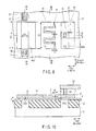
- FIG. 17 shows a plan view of an aging device of the fifth embodiment.
- FIG. 18 is a cross-sectional view along a line XVIII-XVIII in FIG. 17 .
- An element isolation insulating layer 12 with the STI structure is formed in a semiconductor substrate 11.
- First and second element regions (active areas) AA1 and AA2 are surrounded by the element isolation insulating layer 12, and, for example, disposed adjacent to each other in the first direction.
- Diffusion layers 11A and 11B are formed in the first element region AA1.
- the conductivity type of the diffusion layers 11A and 11B is opposite to the conductivity type of the semiconductor substrate 11.
- a floating gate 14 is formed above a channel region between the diffusion layers 11A and 11B.
- An area 13 between the first element region AA1 and the floating gate 14 is filled with a material or remains void.
- a control gate electrode 16 is formed above the second element region AA2.
- An area 15 between the second element region AA2 and the control gate electrode 16 is filled with a material or remains void.
- the floating gate 14 is disposed above the first element region AA1 and above the element isolation insulating layer 12 between the first and second element regions AA1 and AA2.
- the width on the first element region AA1 is L1
- the width in the part adjacent to the control gate electrode 16 is L2 (> L1).
- the floating gate 14 and the control gate electrode 16 are adjacent to each other.
- An area 17A between the floating gate 14 and the control gate electrode 16 is filled with a high-dielectric constant material (High-k material).
- the dielectric constant of the high-dielectric constant material is higher than the dielectric constant of a material or a void filled in the area 13 between the first element region AA1 and the floating gate 14.
- the diffusion layer 11A is connected to a first bit line 19 through a contact plug 18. Meanwhile, the diffusion layer 11B is connected to a second bit line 21 through a contact plug 20.
- the control gate electrode 16 is connected to a word line 23 through a contact plug 22.
- the sixth embodiment is a variation of the fifth embodiment.
- the sixth embodiment is characterized in that a high-dielectric constant material (High-k material) between a floating gate and a control gate electrode is sandwiched with an oxide film, a nitride oxide film, or an oxynitride film, whereby the reliability of an insulating layer is improved.
- High-k material high-dielectric constant material
- FIG. 19 shows a plan view of an aging device in the sixth embodiment.
- FIG. 20 is a cross-sectional view along a line XX-XX in FIG. 19 .
- An element isolation insulating layer 12 with the STI structure is formed in a semiconductor substrate 11.
- First and second element regions (active areas) AA1 and AA2 are surrounded by the element isolation insulating layer 12, and, for example, disposed adjacent to each other in the first direction.
- Diffusion layers 11A and 11B are formed in the first element region AA1.
- the conductivity type of the diffusion layers 11A and 11B is opposite to the conductivity type of the semiconductor substrate 11.
- a floating gate 14 is formed above a channel region between the diffusion layers 11A and 11B.
- An area 13 between the first element region AA1 and the floating gate 14 is filled with a material or remains void.
- a control gate electrode 16 is formed above the second element region AA2.
- An area 15 between the second element region AA2 and the control gate electrode 16 is filled with a material or remains void.
- the floating gate 14 is disposed above the first element region AA1 and above the element isolation insulating layer 12 between the first and second element regions AA1 and AA2.
- the width on the first element region AA1 is L1
- the width in the part adjacent to the control gate electrode 16 is L2 (> L1).
- the floating gate 14 and the control gate electrode 16 are adjacent to each other.
- An area between the floating gate 14 and the control gate electrode 16 is filled with a high-dielectric constant material (High-k material) 17A and insulating materials 17B and 17C.
- High-k material high-dielectric constant material
- the insulating materials 17B and 17C have a function of securing the reliability of both a junction surface between the high-dielectric constant material 17A and the floating gate 14 and a junction surface between the high-dielectric constant material 17A and the control gate electrode 16.
- the insulating materials 17B and 17C are comprised of an oxide film, a nitride oxide film, or an oxynitride film.
- the diffusion layer 11A is connected to a first bit line 19 through a contact plug 18. Meanwhile, the diffusion layer 11B is connected to a second bit line 21 through a contact plug 20.
- the control gate electrode 16 is connected to a word line 23 through a contact plug 22.
- the coupling ratio is rendered large by the high-dielectric constant material, whereby the writing/erasing efficiency is improved.
- first and second element regions AA1 and AA2 are provided in the semiconductor substrate, the second element region AA2 can be omitted in any embodiment.
- the second element region AA2 is replaced with the element isolation insulating layer 12.
- the element isolation insulating layer 12 is disposed directly under the floating gate 14 in the region other than the first element region AA1, and the element isolation insulating layer 12 is disposed also directly under the control gate electrode 16.
- An aging device can be applied to various semiconductor integrated circuits.
- this aging device is promising for a non-volatile semiconductor memory having a single-layer polysilicon type memory cell.
- the aging device of the invention is connected between a non-volatile semiconductor memory and a read device, and reading/writing of data is performed through the aging device of the invention, whereby a period allowing reading/writing of data can be controlled by the aging device.
- the life of the entire non-volatile semiconductor memory can be controlled by one aging device, whereby the variation in the life of each cell does not occur, and, at the same time, the invention can contribute to the increasing of the capacity of the non-volatile semiconductor memory.
- an aging device suitable for high-speed writing/erasing can be realized.
Landscapes
- Engineering & Computer Science (AREA)
- Microelectronics & Electronic Packaging (AREA)
- Physics & Mathematics (AREA)
- General Physics & Mathematics (AREA)
- Non-Volatile Memory (AREA)
- Semiconductor Memories (AREA)
- Read Only Memory (AREA)
- Insulated Gate Type Field-Effect Transistor (AREA)
Applications Claiming Priority (1)
| Application Number | Priority Date | Filing Date | Title |
|---|---|---|---|
| JP2007186343A JP4455621B2 (ja) | 2007-07-17 | 2007-07-17 | エージングデバイス |
Publications (2)
| Publication Number | Publication Date |
|---|---|
| EP2017880A2 true EP2017880A2 (de) | 2009-01-21 |
| EP2017880A3 EP2017880A3 (de) | 2009-05-27 |
Family
ID=39734093
Family Applications (1)
| Application Number | Title | Priority Date | Filing Date |
|---|---|---|---|
| EP08160605A Withdrawn EP2017880A3 (de) | 2007-07-17 | 2008-07-17 | Festkörperzeitmessvorrichtung mit einem Schwebegattertransistor |
Country Status (5)
| Country | Link |
|---|---|
| US (1) | US7977729B2 (de) |
| EP (1) | EP2017880A3 (de) |
| JP (1) | JP4455621B2 (de) |
| KR (1) | KR20090008144A (de) |
| CN (1) | CN101350350A (de) |
Families Citing this family (9)
| Publication number | Priority date | Publication date | Assignee | Title |
|---|---|---|---|---|
| JP4435095B2 (ja) * | 2006-01-04 | 2010-03-17 | 株式会社東芝 | 半導体システム |
| US8692310B2 (en) | 2009-02-09 | 2014-04-08 | Spansion Llc | Gate fringing effect based channel formation for semiconductor device |
| US8755229B1 (en) | 2009-06-23 | 2014-06-17 | Micron Technology, Inc. | Limiting flash memory over programming |
| EP2819065B1 (de) | 2013-06-27 | 2015-10-28 | Nxp B.V. | Zeitreferenz ohne Energieversorgung |
| US20150137201A1 (en) * | 2013-11-20 | 2015-05-21 | Qualcomm Incorporated | High density linear capacitor |
| KR102373596B1 (ko) * | 2015-11-23 | 2022-03-14 | 에스케이하이닉스 주식회사 | 수평적 커플링 구조를 갖는 불휘발성 메모리셀 및 이를 이용한 메모리 셀 어레이 |
| US9847133B2 (en) * | 2016-01-19 | 2017-12-19 | Ememory Technology Inc. | Memory array capable of performing byte erase operation |
| FR3054885B1 (fr) * | 2016-08-03 | 2018-09-07 | Stmicroelectronics (Crolles 2) Sas | Procede d'estimation d'un profil d'exploitation d'un circuit integre d'un systeme sur puce, et systeme sur puce correspondant |
| AU2017330515A1 (en) * | 2016-09-22 | 2019-05-16 | Integrated Tactical Technologies, Llc | Two-way communication system and method of use |
Citations (3)
| Publication number | Priority date | Publication date | Assignee | Title |
|---|---|---|---|---|
| JP2004172404A (ja) | 2002-11-20 | 2004-06-17 | Toshiba Corp | 半導体集積回路 |
| JP2005310824A (ja) | 2004-04-16 | 2005-11-04 | Toshiba Corp | 半導体装置 |
| JP2007184321A (ja) | 2006-01-04 | 2007-07-19 | Toshiba Corp | 半導体装置と半導体システム |
Family Cites Families (18)
| Publication number | Priority date | Publication date | Assignee | Title |
|---|---|---|---|---|
| US6009013A (en) * | 1992-01-29 | 1999-12-28 | Interuniversitair Micro-Elektronica Centrum Vzw | Contactless array configuration for semiconductor memories |
| US6252271B1 (en) * | 1998-06-15 | 2001-06-26 | International Business Machines Corporation | Flash memory structure using sidewall floating gate and method for forming the same |
| JP3622536B2 (ja) * | 1998-11-18 | 2005-02-23 | 株式会社デンソー | 不揮発性半導体記憶装置の製造方法 |
| US6133098A (en) * | 1999-05-17 | 2000-10-17 | Halo Lsi Design & Device Technology, Inc. | Process for making and programming and operating a dual-bit multi-level ballistic flash memory |
| JP2001338994A (ja) * | 2000-05-29 | 2001-12-07 | Matsushita Electric Ind Co Ltd | 半導体記憶装置及びその製造方法 |
| US6747308B2 (en) * | 2001-12-28 | 2004-06-08 | Texas Instruments Incorporated | Single poly EEPROM with reduced area |
| US6780712B2 (en) * | 2002-10-30 | 2004-08-24 | Taiwan Semiconductor Manufacturing Company | Method for fabricating a flash memory device having finger-like floating gates structure |
| JP4016679B2 (ja) * | 2002-03-11 | 2007-12-05 | 株式会社デンソー | 半導体装置及び半導体装置の製造方法 |
| JP4068519B2 (ja) * | 2002-07-08 | 2008-03-26 | 株式会社東芝 | 有効期限付き機能利用装置 |
| US7075284B2 (en) * | 2002-07-08 | 2006-07-11 | Kabushiki Kaisha Toshiba | Time limit function utilization |
| US6853583B2 (en) | 2002-09-16 | 2005-02-08 | Impinj, Inc. | Method and apparatus for preventing overtunneling in pFET-based nonvolatile memory cells |
| JP3927156B2 (ja) * | 2003-02-26 | 2007-06-06 | 株式会社東芝 | 不揮発性半導体記憶装置 |
| JP4005962B2 (ja) * | 2003-09-22 | 2007-11-14 | 株式会社東芝 | 不揮発性半導体記憶装置 |
| US20060081910A1 (en) * | 2004-03-16 | 2006-04-20 | Andy Yu | Non-volatile electrically alterable memory cell for storing multiple data and an array thereof |
| KR100780661B1 (ko) | 2005-06-29 | 2007-11-29 | 주식회사 하이닉스반도체 | 비휘발성 메모리 소자의 유전체막 및 그 형성방법 |
| JP4891667B2 (ja) * | 2005-08-22 | 2012-03-07 | 株式会社東芝 | 半導体装置の製造方法 |
| JP4282705B2 (ja) | 2006-09-28 | 2009-06-24 | 株式会社東芝 | エージングデバイス及びその製造方法 |
| JP2008305819A (ja) * | 2007-06-05 | 2008-12-18 | Sanken Electric Co Ltd | 不揮発性半導体記憶装置およびその製造方法 |
-
2007
- 2007-07-17 JP JP2007186343A patent/JP4455621B2/ja not_active Expired - Fee Related
-
2008
- 2008-07-15 US US12/173,535 patent/US7977729B2/en not_active Expired - Fee Related
- 2008-07-16 KR KR1020080068912A patent/KR20090008144A/ko not_active Ceased
- 2008-07-17 EP EP08160605A patent/EP2017880A3/de not_active Withdrawn
- 2008-07-17 CN CNA2008101379683A patent/CN101350350A/zh active Pending
Patent Citations (3)
| Publication number | Priority date | Publication date | Assignee | Title |
|---|---|---|---|---|
| JP2004172404A (ja) | 2002-11-20 | 2004-06-17 | Toshiba Corp | 半導体集積回路 |
| JP2005310824A (ja) | 2004-04-16 | 2005-11-04 | Toshiba Corp | 半導体装置 |
| JP2007184321A (ja) | 2006-01-04 | 2007-07-19 | Toshiba Corp | 半導体装置と半導体システム |
Also Published As
| Publication number | Publication date |
|---|---|
| US20090020803A1 (en) | 2009-01-22 |
| US7977729B2 (en) | 2011-07-12 |
| JP2009026832A (ja) | 2009-02-05 |
| CN101350350A (zh) | 2009-01-21 |
| KR20090008144A (ko) | 2009-01-21 |
| JP4455621B2 (ja) | 2010-04-21 |
| EP2017880A3 (de) | 2009-05-27 |
Similar Documents
| Publication | Publication Date | Title |
|---|---|---|
| US7977729B2 (en) | Aging device | |
| US7915666B2 (en) | Nonvolatile semiconductor memory devices with charge injection corner | |
| CN100334734C (zh) | 半导体存储单元和半导体存储装置 | |
| US5412600A (en) | Non-volatile semiconductor device with selecting transistor formed between adjacent memory transistors | |
| WO2007114955A2 (en) | Methods for erasing and programming memory devices | |
| US7525149B2 (en) | Combined volatile and non-volatile memory device with graded composition insulator stack | |
| KR100695702B1 (ko) | Ic 카드 | |
| US7595237B2 (en) | Non-volatile memory cell with a hybrid access transistor | |
| CN101506968A (zh) | 屏蔽浮栅隧穿元件结构 | |
| EP0443515B1 (de) | Nichtflüchtige Halbleitervorrichtung | |
| US6774428B1 (en) | Flash memory structure and operating method thereof | |
| KR20040031655A (ko) | 단일비트 비휘발성 메모리셀 및 그것의 프로그래밍 및삭제방법 | |
| US20030075773A1 (en) | Semiconductor memory device | |
| JP3175665B2 (ja) | 不揮発性半導体記憶装置のデータ消去方法 | |
| CN102027588A (zh) | 具有eeprom结构的只读存储器 | |
| KR100908755B1 (ko) | 전하 축적층을 갖는 mis 트랜지스터를 구비한 반도체기억 장치 | |
| CN107863344A (zh) | 半导体存储器以及半导体存储器的制造方法 | |
| US10797063B2 (en) | Single-poly nonvolatile memory unit | |
| CN101030581B (zh) | Eeprom | |
| JP3375087B2 (ja) | 半導体記憶装置およびその記憶情報読出方法 | |
| JP7462389B2 (ja) | 不揮発性半導体記憶装置 | |
| JP2006332143A (ja) | 半導体装置及びその製造方法 | |
| JP2025001760A (ja) | 半導体装置 | |
| JPWO2010038426A1 (ja) | 浮遊ゲート型不揮発性メモリ配置構成 | |
| KR20100055050A (ko) | 플래시 메모리 셀, 그 독출방법 및 제조방법 |
Legal Events
| Date | Code | Title | Description |
|---|---|---|---|
| PUAI | Public reference made under article 153(3) epc to a published international application that has entered the european phase |
Free format text: ORIGINAL CODE: 0009012 |
|
| 17P | Request for examination filed |
Effective date: 20080717 |
|
| AK | Designated contracting states |
Kind code of ref document: A2 Designated state(s): AT BE BG CH CY CZ DE DK EE ES FI FR GB GR HR HU IE IS IT LI LT LU LV MC MT NL NO PL PT RO SE SI SK TR |
|
| AX | Request for extension of the european patent |
Extension state: AL BA MK RS |
|
| PUAL | Search report despatched |
Free format text: ORIGINAL CODE: 0009013 |
|
| AK | Designated contracting states |
Kind code of ref document: A3 Designated state(s): AT BE BG CH CY CZ DE DK EE ES FI FR GB GR HR HU IE IS IT LI LT LU LV MC MT NL NO PL PT RO SE SI SK TR |
|
| AX | Request for extension of the european patent |
Extension state: AL BA MK RS |
|
| AKX | Designation fees paid |
Designated state(s): DE FR GB |
|
| 17Q | First examination report despatched |
Effective date: 20100209 |
|
| STAA | Information on the status of an ep patent application or granted ep patent |
Free format text: STATUS: THE APPLICATION IS DEEMED TO BE WITHDRAWN |
|
| 18D | Application deemed to be withdrawn |
Effective date: 20100622 |