EP2017881A2 - Verfahren zur Herstellung einer aktiven Halbleiterschicht, Herstellungsverfahren für einen Dünnfilm-Transistor, der diese verwendet und Dünnfilm-Transistor mit aktiver Halbleiterschicht - Google Patents
Verfahren zur Herstellung einer aktiven Halbleiterschicht, Herstellungsverfahren für einen Dünnfilm-Transistor, der diese verwendet und Dünnfilm-Transistor mit aktiver Halbleiterschicht Download PDFInfo
- Publication number
- EP2017881A2 EP2017881A2 EP08160476A EP08160476A EP2017881A2 EP 2017881 A2 EP2017881 A2 EP 2017881A2 EP 08160476 A EP08160476 A EP 08160476A EP 08160476 A EP08160476 A EP 08160476A EP 2017881 A2 EP2017881 A2 EP 2017881A2
- Authority
- EP
- European Patent Office
- Prior art keywords
- target
- atomic
- active layer
- igzo
- thin film
- Prior art date
- Legal status (The legal status is an assumption and is not a legal conclusion. Google has not performed a legal analysis and makes no representation as to the accuracy of the status listed.)
- Granted
Links
Images


Classifications
-
- C—CHEMISTRY; METALLURGY
- C23—COATING METALLIC MATERIAL; COATING MATERIAL WITH METALLIC MATERIAL; CHEMICAL SURFACE TREATMENT; DIFFUSION TREATMENT OF METALLIC MATERIAL; COATING BY VACUUM EVAPORATION, BY SPUTTERING, BY ION IMPLANTATION OR BY CHEMICAL VAPOUR DEPOSITION, IN GENERAL; INHIBITING CORROSION OF METALLIC MATERIAL OR INCRUSTATION IN GENERAL
- C23C—COATING METALLIC MATERIAL; COATING MATERIAL WITH METALLIC MATERIAL; SURFACE TREATMENT OF METALLIC MATERIAL BY DIFFUSION INTO THE SURFACE, BY CHEMICAL CONVERSION OR SUBSTITUTION; COATING BY VACUUM EVAPORATION, BY SPUTTERING, BY ION IMPLANTATION OR BY CHEMICAL VAPOUR DEPOSITION, IN GENERAL
- C23C14/00—Coating by vacuum evaporation, by sputtering or by ion implantation of the coating forming material
- C23C14/06—Coating by vacuum evaporation, by sputtering or by ion implantation of the coating forming material characterised by the coating material
- C23C14/08—Oxides
- C23C14/086—Oxides of zinc, germanium, cadmium, indium, tin, thallium or bismuth
-
- C—CHEMISTRY; METALLURGY
- C23—COATING METALLIC MATERIAL; COATING MATERIAL WITH METALLIC MATERIAL; CHEMICAL SURFACE TREATMENT; DIFFUSION TREATMENT OF METALLIC MATERIAL; COATING BY VACUUM EVAPORATION, BY SPUTTERING, BY ION IMPLANTATION OR BY CHEMICAL VAPOUR DEPOSITION, IN GENERAL; INHIBITING CORROSION OF METALLIC MATERIAL OR INCRUSTATION IN GENERAL
- C23C—COATING METALLIC MATERIAL; COATING MATERIAL WITH METALLIC MATERIAL; SURFACE TREATMENT OF METALLIC MATERIAL BY DIFFUSION INTO THE SURFACE, BY CHEMICAL CONVERSION OR SUBSTITUTION; COATING BY VACUUM EVAPORATION, BY SPUTTERING, BY ION IMPLANTATION OR BY CHEMICAL VAPOUR DEPOSITION, IN GENERAL
- C23C14/00—Coating by vacuum evaporation, by sputtering or by ion implantation of the coating forming material
- C23C14/22—Coating by vacuum evaporation, by sputtering or by ion implantation of the coating forming material characterised by the process of coating
- C23C14/34—Sputtering
- C23C14/3464—Sputtering using more than one target
-
- H—ELECTRICITY
- H10—SEMICONDUCTOR DEVICES; ELECTRIC SOLID-STATE DEVICES NOT OTHERWISE PROVIDED FOR
- H10D—INORGANIC ELECTRIC SEMICONDUCTOR DEVICES
- H10D30/00—Field-effect transistors [FET]
- H10D30/60—Insulated-gate field-effect transistors [IGFET]
- H10D30/67—Thin-film transistors [TFT]
- H10D30/674—Thin-film transistors [TFT] characterised by the active materials
- H10D30/6755—Oxide semiconductors, e.g. zinc oxide, copper aluminium oxide or cadmium stannate
-
- H—ELECTRICITY
- H10—SEMICONDUCTOR DEVICES; ELECTRIC SOLID-STATE DEVICES NOT OTHERWISE PROVIDED FOR
- H10P—GENERIC PROCESSES OR APPARATUS FOR THE MANUFACTURE OR TREATMENT OF DEVICES COVERED BY CLASS H10
- H10P14/00—Formation of materials, e.g. in the shape of layers or pillars
- H10P14/20—Formation of materials, e.g. in the shape of layers or pillars of semiconductor materials
- H10P14/22—Formation of materials, e.g. in the shape of layers or pillars of semiconductor materials using physical deposition, e.g. vacuum deposition or sputtering
-
- H—ELECTRICITY
- H10—SEMICONDUCTOR DEVICES; ELECTRIC SOLID-STATE DEVICES NOT OTHERWISE PROVIDED FOR
- H10P—GENERIC PROCESSES OR APPARATUS FOR THE MANUFACTURE OR TREATMENT OF DEVICES COVERED BY CLASS H10
- H10P14/00—Formation of materials, e.g. in the shape of layers or pillars
- H10P14/20—Formation of materials, e.g. in the shape of layers or pillars of semiconductor materials
- H10P14/29—Formation of materials, e.g. in the shape of layers or pillars of semiconductor materials characterised by the substrates
- H10P14/2901—Materials
- H10P14/2922—Materials being non-crystalline insulating materials, e.g. glass or polymers
-
- H—ELECTRICITY
- H10—SEMICONDUCTOR DEVICES; ELECTRIC SOLID-STATE DEVICES NOT OTHERWISE PROVIDED FOR
- H10P—GENERIC PROCESSES OR APPARATUS FOR THE MANUFACTURE OR TREATMENT OF DEVICES COVERED BY CLASS H10
- H10P14/00—Formation of materials, e.g. in the shape of layers or pillars
- H10P14/20—Formation of materials, e.g. in the shape of layers or pillars of semiconductor materials
- H10P14/34—Deposited materials, e.g. layers
- H10P14/3402—Deposited materials, e.g. layers characterised by the chemical composition
- H10P14/3424—Deposited materials, e.g. layers characterised by the chemical composition being Group IIB-VIA materials
- H10P14/3426—Oxides
-
- H—ELECTRICITY
- H10—SEMICONDUCTOR DEVICES; ELECTRIC SOLID-STATE DEVICES NOT OTHERWISE PROVIDED FOR
- H10P—GENERIC PROCESSES OR APPARATUS FOR THE MANUFACTURE OR TREATMENT OF DEVICES COVERED BY CLASS H10
- H10P14/00—Formation of materials, e.g. in the shape of layers or pillars
- H10P14/20—Formation of materials, e.g. in the shape of layers or pillars of semiconductor materials
- H10P14/34—Deposited materials, e.g. layers
- H10P14/3402—Deposited materials, e.g. layers characterised by the chemical composition
- H10P14/3434—Deposited materials, e.g. layers characterised by the chemical composition being oxide semiconductor materials
Definitions
- Embodiments relate to a method of manufacturing a semiconductor active layer, a method of manufacturing a thin film transistor using the same, and a thin film transistor including the semiconductor active layer.
- a semiconductor layer using amorphous silicon or polysilicon has recently been developed for use in a thin film transistor (TFT) for light emitting display devices such as organic light emitting display devices, which use organic light emitting diodes (OLEDs) to emit light.
- TFT thin film transistor
- OLEDs organic light emitting diodes
- the semiconductor layer When the semiconductor layer is formed of amorphous silicon, the semiconductor layer may exhibit low mobility. The use of such a low mobility layer as a drive circuit of a display panel that requires a fast response time may be difficult.
- Polysilicon may be used as the semiconductor layer to provide high mobility, but the threshold voltage of the TFT may not be uniform. Additionally, leakage current may occur in the amorphous silicon or polysilicon semiconductor layer when light, e.g., light from a backlight unit, is incident thereon.
- Oxide-based semiconductors may exhibit a band gap that is higher than the light energy in a visible light region. Accordingly, an oxide-based semiconductor may exhibit little or no leakage current resulting from visible light absorption. Therefore, the use of oxide-based semiconductors, e.g., semiconductors having an indium-gallium-zinc oxide (hereinafter, "IGZO") active layer, has been proposed as a solution to problems in the art. However, there is a need for further developments in the formation of an IGZO active layer, e.g., to provide control over the atomic composition thereof and improve the electrical characteristics of devices including the IGZO active layer.
- IGZO indium-gallium-zinc oxide
- Embodiments are therefore directed to a method of manufacturing a semiconductor active layer, a method of manufacturing a thin film transistor using the same, and a thin film transistor including the semiconductor active layer, which substantially overcome one or more of the problems due to the limitations and disadvantages of the related art.
- At least one of the above and other features and advantages may be realized by providing a method of manufacturing an IGZO active layer, the method including depositing ions including In, Ga, and Zn from a first target, and depositing ions including In from a second target having a different atomic composition from the first target.
- the deposition of ions from the second target may be controlled to adjust an atomic% of In in the IGZO layer to be about 45 atomic% to about 80 atomic%.
- the atomic% of In in the IGZO layer may be about 55 atomic% to about 75 atomic%.
- the atomic% of In in the IGZO layer may be about 60 atomic% to about 70 atomic%.
- the first target may include In, Ga, and Zn in a molar ratio of about 1:1:1.
- the first target may be made of InGaZnO, and the second target is made of InZnO.
- the first target may include In, Ga, and Zn in a molar ratio of about 1:1:1, and the second target may includes In and Zn in a molar ratio of about 1:1 to about 6:1 (In:Zn).
- the atomic% of In in the IGZO layer may be adjusted by adjusting a molar ratio of In:Zn in the second target.
- First and second bias powers may be applied to the first target and the second target, respectively, and the atomic% of In in the IGZO layer may be adjusted by adjusting the intensity of the second bias power.
- the first target and the second target may be irradiated with first and second pulsed lasers, and the atomic% of In in the IGZO layer may be adjusted by adjusting the intensity of the second pulsed laser.
- At least one of the above and other features and advantages may also be realized by providing a method of manufacturing a thin film transistor, the method including forming an IGZO active layer on a substrate, forming a gate electrode spaced apart from the IGZO active layer by a gate dielectric layer, forming a source electrode that contacts a first portion of the IGZO active layer, and forming a drain electrode that contacts a second portion of the IGZO active layer.
- Forming the IGZO active layer may include depositing ions including In, Ga, and Zn from a first target, and depositing ions including In from a second target having a different atomic composition from the first target, the deposition of ions from the second target being controlled to adjust an atomic% of In in the IGZO layer to be about 45 atomic% to about 80 atomic%.
- the atomic% of In in the IGZO layer may be about 55 atomic% to about 75 atomic%.
- the atomic% of In in the IGZO layer may be about 60 atomic% to about 70 atomic%.
- the first target may include In, Ga, and Zn in a molar ratio of about 1:1:1.
- the first target may be made of InGaZnO
- the second target may be made of InZnO.
- the first target may include In, Ga, and Zn in a molar ratio of about 1:1:1, and the second target may include In and Zn in a molar ratio of about 1:1 to about 6:1 (In:Zn).
- the atomic% of In in the IGZO layer may be adjusted by adjusting a molar ratio of In:Zn in the second target.
- First and second bias powers may be applied to the first target and the second target, respectively, and the atomic% of In in the IGZO layer may be adjusted by adjusting the intensity of the second bias power.
- the first target and the second target may be irradiated with first and second pulsed lasers, and the atomic% of In in the IGZO layer may be adjusted by adjusting the intensity of the second pulsed laser.
- the gate dielectric layer may be on the gate electrode such that the gate electrode is between the gate dielectric layer and the substrate, and the IGZO active layer may be on the gate dielectric layer.
- the gate dielectric layer may be on the IGZO active layer such that the IGZO active layer is between the gate dielectric layer and the substrate, and the gate electrode may be on the gate dielectric layer.
- a thin film transistor including a substrate, an IGZO active layer on the substrate, the IGZO layer including a channel region, a source region, and a drain region, a gate electrode overlapping the channel region and insulated from the active layer by a gate insulator, and source and drain electrodes contacting the source and drain regions, respectively.
- An atomic% of In in the IGZO active layer may be about 45 atomic% to about 80 atomic%.
- the atomic% of In in the IGZO active layer may be about 55 atomic% to about 75 atomic%.
- each of the expressions “at least one of A, B, and C,” “at least one of A, B, or C,” “one or more of A, B, and C,” “one or more of A, B, or C” and "A, B, and/or C” includes the following meanings: A alone; B alone; C alone; both A and B together; both A and C together; both B and C together; and all three of A, B, and C together.
- the expression “or” is not an “exclusive or” unless it is used in conjunction with the term “either.”
- the expression “A, B, or C” includes A alone; B alone; C alone; both A and B together; both A and C together; both B and C together; and all three of A, B and, C together
- the expression “either A, B, or C” means one of A alone, B alone, and C alone, and does not mean any of both A and B together; both A and C together; both B and C together; and all three of A, B and C together.
- a gas may represent a single component, e.g., argon, or multiple components in combination, e.g., argon mixed with oxygen.
- atomic ratio and “molar ratio” are synonymous. Additionally, the terms “atomic percentage” and “atomic%” indicate the amount of one of indium (In), gallium (Ga), or zinc (Zn) relative to amount of indium, gallium and zinc combined, unless indicated otherwise.
- Embodiments may provide a method of manufacturing a semiconductor active layer capable of increasing an atomic% of indium (In) in an IGZO semiconductor active layer.
- the mobility of a carrier (electrons) may increase if the relative amount of indium (In) is increased, and a concentration of the carrier (electrons) may decrease if the relative amount of gallium (Ga) is increased.
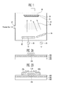
- FIG. 1 illustrates a schematic view of a codeposition apparatus according to an embodiment.
- ions of In, Ga and Zn may be deposited from a first target 22, e.g., a target made of InGaZnO, to form an IGZO layer 31 on a substrate 30, and ions of In may be deposited from a second target 24, e.g., a target made of InZnO, to adjust a compositional ratio of In in the IGZO layer.
- a first target 22 e.g., a target made of InGaZnO
- a target made of InZnO e.g., a target made of InZnO
- two targets 22 and 24, e.g., an InGaZnO target and an InZnO target may be used to suitably control the atomic ratio of cations such as In, Ga and Zn in the active layer. This may provide better control over the compositional ratio of In, Ga and Zn cations in the IGZO layer
- FIG. 1 illustrates a cosputtering apparatus. It will be appreciated that other physical deposition operations, e.g., electron beam sputtering, pulsed laser deposition, etc., may also be used.
- the first target 22 and the second target 24 may be disposed at one side of the inside of a chamber 10 having a gas inlet 12 and a gas outlet (not shown) formed therein.
- a first bias power 23 and a second bias power 25 may be applied to the first target 22 and the second target 24, respectively.
- a plate 26 may support the substrate 30, and may be disposed inside of the chamber 10 to face the first target 22 and the second target 24.
- the plate 26 may be coupled to a grounding conductor. In an implementation, the potential of the plate 26 may be varied depending on whether the first bias power 23 and the second bias power 25 are applied.
- An inert gas, e.g., argon (Ar), and a carrier gas, e.g., oxygen (O 2 ), may be supplied as a process gas into the chamber 10 through the gas inlet 12.
- the amount of oxygen (O 2 ) supplied may be adjusted according to the desired electrical characteristics of the semiconductor active layer.
- a concentration of the carrier may be adjusted by adjusting the partial pressure of oxygen (O 2 ) in the process gas. For example, the concentration of the carrier may be decreased if the partial pressure of oxygen (O 2 ) is increased, and the concentration of the carrier may be increased if the partial pressure of oxygen (O 2 ) is decreased.
- the first bias power 23 and the second bias power 25 may be applied to the InGaZnO target 22 and the InZnO target 24, respectively, while the process gas is supplied.
- An electric field may be formed between the plate 26 and the InGaZnO target 22 and InZnO target 24, and a high density plasma 28 may be generated by the bombardment of process gas molecules with electrons accelerated by an applied electromagnetic field.
- Cations of In, Ga and Zn may be deposited from the InGaZnO target 22, and cations of In and Zn may be deposited from the InZnO target 24 by the plasma 28 using a sputtering operation so as to form the IGZO active layer 31 on the substrate 30.
- the compositional ratio (atomic%) of the cations of In, Ga, and Zn may be controlled according to the respective intensities of the first bias power 23 and the second bias power 25.
- the compositional ratio of In in the IGZO active layer 31 may be adjusted by increasing a speed for deposition of In and Zn ions from the InZnO target 24, e.g., a sputtering rate of the InZnO target 24 may be increased more than that of the InGaZnO target 22 by adjusting the intensity of the second bias power 25.
- the amount of Ga in the IGZO active layer 31 may be set to about 10 atomic% or more. This may reduce or avoid the formation of excess carriers that may lead to unstable electrical characteristics, e.g., an increased OFF current or variations in threshold voltage.
- the compositional ratio (atomic%) of the cations of In, Ga, and Zn may be controlled by adjusting the molar ratios of these elements in the InGaZnO target 22 and/or the InZnO target 24.
- the InGaZnO target 22 preferably consists of an indium gallium zinc oxide composition and the contents of indium, gallium and zinc can be modified.
- the InZnO target 24 preferably consists of an indium zinc oxide composition, wherein the contents of indium and zinc can be modified.
- the molar ratio of In:Ga:Zn in the InGaZnO target 22 may be about 1:1:1, and the compositional ratio of In in the IGZO active layer 31 may be adjusted to about 45 atomic% to about 80 atomic% by increasing the amount of In in the InZnO target 24.
- the molar ratio of In:Zn in the InZnO target 24 may be about 1:1 to about 6:1 (In:Zn).
- the compositional ratio of In in the IGZO active layer may be about 55 atomic% to about 75 atomic%, or about 60 atomic% to about 70 atomic%.
- an electron beam sputtering apparatus may be used. Cations of In, Ga, and Zn may be deposited from the InGaZnO target 22 and the InZnO target 24 by irradiating the InGaZnO target 22 and the InZnO target 24 with first and second electron beams (not shown), thereby forming the IGZO active layer 31 on the substrate 30.
- the compositional ratio of the cations of In, Ga, and Zn in the IGZO active layer 31 may be adjusted according to the intensity of the first and second electron beams and/or the molar ratio of In, Ga, and Zn in the InGaZnO target 22 and the molar ratio of In and Zn in the InZnO target 24.
- a pulsed laser deposition apparatus may be used. Cations of In, Ga, and Zn may be deposited from the InGaZnO target 22 and the InZnO target 24 by irradiating the InGaZnO target 22 and the InZnO target 24 with first and second pulsed lasers (not shown), thereby forming the IGZO active layer 31 on the substrate 30.
- the compositional ratio of the cations of In, Ga, and Zn in the IGZO active layer 31 may be adjusted according to the intensity of the first and second pulsed lasers and/or the molar ratio of In, Ga, and Zn in the InGaZnO target 22 and the molar ratio of In and Zn in the InZnO target 24.
- the IGZO active layer 31 manufactured according to embodiments may have a composition where the cations are spatially non-uniform due to the use of two targets 22, 24.
- the relative ratio of In:Ga:Zn in the IGZO active layer 31 may vary across the substrate 30, i.e., it may vary according to (x, y) coordinates when mapped along X and Y axes that are parallel to the substrate 30. Therefore, the IGZO active layer 31 according to an embodiment may exhibit structural differences from an IGZO layer manufactured using a single target of InGaZnO.
- FIGS. 2A and 2B illustrate cross-sectional views of stages in a method of manufacturing a bottom gate (an inverted staggered bottom gate) thin film transistor according to an embodiment.
- a buffer layer 102 may be formed on a substrate 100, and a gate electrode 104 may be formed on the buffer layer 102.
- a gate insulator 106 may be formed on the buffer layer 102 and on the gate electrode 104.
- an IGZO active layer 108 providing a channel region, a source region and a drain region may be formed on the gate insulator 106.
- the active layer 108 may be formed according to an embodiment, e.g., as described above in connection with FIG. 1 .
- the IGZO active layer may be formed on the substrate 100 by depositing ions, including In, Ga and Zn, from the InGaZnO target 22 and the InZnO target 24.
- the compositional ratio of In may be adjusted to, e.g., about 45 atomic% to about 80 atomic%, e.g., by adjusting the intensity of a bias power, adjusting the intensity of an electron beam or a pulse laser, or adjusting the molar ratios of the components of the InGaZnO target 22 and/or InZnO target 24.
- the IGZO active layer 108 may then be patterned, and source and drain electrodes 110a and 110b may be formed to contact the respective source and drain regions of the IGZO active layer 108.
- a buffer layer was formed as a silicon oxide film (SiO x ) on a glass substrate, and 200 nm-thick tungsten molybdenum (MoW) was deposited thereon and then patterned to form a gate electrode on the buffer layer.
- the lateral dimensions of the gate electrode were 70 mm ⁇ 70 mm.
- a 200 nm-thick silicon nitride film (SiN x ) was deposited at a temperature of 330 °C using a plasma-enhanced chemical vapor deposition (PECVD) operation to form a gate insulator on the buffer layer and on the gate electrode.
- PECVD plasma-enhanced chemical vapor deposition
- An IGZO active layer was formed on the gate insulator in an ambient temperature using a cosputtering apparatus.
- An amorphous phase of the IGZO active layer was formed having a thickness of 50 nm.
- the width and length of the channel region of the active layer were 1000 ⁇ m and 150 ⁇ m, respectively.
- a first target of In 2 Ga 2 ZnO 7 i.e., InGaZnO
- a second target of In 2 O 3 -10wt%ZnO 90 weight% In 2 O 3 and 10 weight% ZnO
- the internal pressure of the process chamber in the cosputtering apparatus was maintained at about 5 mTorr, and argon (Ar) and oxygen (O 2 ) were supplied as the process gas at a ratio of 65:35 (Ar:O 2 ).
- a radiofrequency (RF) bias power of 450 W was applied to the first target of In 2 Ga 2 ZnO 7 , and a RF bias power of from 0 W to 700 W was applied to the second target of In 2 O 3 -10wt%ZnO.
- the IGZO active layer was patterned and a 200 nm-thick transparent electrode material of indium zinc oxide (IZO) was deposited at ambient temperature.
- the electrode material was then patterned to form source and drain electrodes and on the entire upper surface, so that the source and drain electrodes were in contact with the source and drain regions, respectively, of the IGZO active layer.
- a shadow mask was used for the patterning operation, and the thin film transistor thus manufactured was heat-treated at a temperature of 350 °C for 1 hour.
- FIGS. 3A and 3B illustrate graphs showing transfer characteristics of thin film transistors manufactured according to the above-described operations.
- a semiconductor parameter analyzer (Agilent 4156C) was used to analyze electrical characteristics of the example thin film transistors (measurements were carried out at ambient temperature).
- FIG. 3A illustrates the results for a thin film transistor manufactured using a bias power of 0 W applied to the In 2 O 3 -10wt%ZnO target.
- FIG. 3B illustrates the results for a thin film transistor manufactured using a bias power of 400 W applied to the In 2 O 3 -10wt%ZnO target.
- V T,sat For a drain voltage (V DS ) of 5.1V and an electric current of L/W ⁇ 10 nA flowing through the drain electrode, the threshold voltage (V T,sat ) is defined by a voltage applied to the gate electrode.
- ⁇ FE L ⁇ g m W ⁇ C i ⁇ V DS
- Equation 1 C i and g m are gate capacitance and transconductance per unit area, respectively.
- L and w are length and width, respectively.
- a slope factor S (S factor) may be calculated from the transfer characteristics, as shown in the following Equation 2.
- S d ⁇ V GS d log I DS
- I DS is the saturated drain current
- V GS is the voltage between the gate and source.
- N t S ⁇ log e / kT / q - 1 ⁇ C i q
- N-channel conductivity having a mobility ( ⁇ FE ) of 11.2 ⁇ 2.0 cm 2 /Vs was observed in the thin film transistor.
- the slope factor S (S factor) and the ON/OFF current ratio (I on/off ) were 1.11 ⁇ 0.06 V/dec and ⁇ 6.6 ⁇ 10 6 , respectively.
- FIGS. 3C and 3D show the results obtained by measuring output characteristics of the thin film transistor manufactured according to the above-described operations.
- FIG. 3C shows the results for a bias power of 0 W applied to the second target, i.e., the In 2 O 3 -10wt%ZnO target.
- FIG. 3D shows the results for a bias power of 400 W applied to the second target.
- the thin film transistor according to an embodiment showed pinch-off and saturation characteristics as in the case of the field effect transistor (FET).
- FET field effect transistor
- An organic light emitting display apparatus requires a drain current (I DS ) of about 1 ⁇ A to display full white grayscale.
- the thin film transistor When the bias power applied to the second target was 0 W, the thin film transistor had a saturated drain current (I DS ) of about 1.0 ⁇ A when a voltage (V GS ) between the gate and source was 8 V. When the bias power applied to the second target was 400 W, the thin film transistor had a saturated drain current (I DS ) of about 1.0 ⁇ A when a voltage (V GS ) between the gate and source was 1V ⁇ 4V.
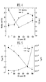
- FIG. 4 illustrates a graph of mobility ( ⁇ FE ) and slope factor S characteristics of the thin film transistor with respect to the bias power applied to the second target, i.e., the In 2 O 3 -10wt%ZnO ("InZnO") target.
- the mobility ( ⁇ FE ) generally increased as the bias power applied to the InZnO target increased.
- the bias power increased up to 600 W
- the mobility increased to 24.0 ⁇ 0.64 cm 2 /Vs.
- the mobility slightly decreased, to 21.7 ⁇ 1.39 cm 2 /Vs when the bias power was 700 W.
- FIG. 5 illustrates a graph of threshold voltage (V T , sat ) and leakage current (OFF current I OFF ) characteristics with respect to the bias power applied to the second target, i.e., the InZnO target.
- the threshold voltage (V T,Sat ) may be controlled according to the bias power applied to the InZnO target.
- the bias power is preferably adjusted to 600 W or less, since leakage current increases rapidly if the bias power is increased up to 700 W or more.
- the threshold voltage (V T,Sat ) slowly decreased.
- the thin film transistor changed from accumulation mode to depletion mode (threshold voltage (V T,sat ) of - 12.1 ⁇ 1.91 V) when the bias power was 700 W.
- the decrease in the mobility ( ⁇ FE ) associated with the high bias power applied to the second target, i.e., the InZnO target, shown in FIG. 4 is due to the bombardment of ions having a high energy during the sputtering operation. Interfacial characteristics with a bottom gate insulator may be deteriorated by the bombardment of strong ions. Also, the generation of deep level defects by the bombardment of ions under the high bias power condition and/or incorporation of sputtering ions such as argon (Ar+) in the thin film may adversely affect the device characteristics. Evidence of such is shown by the changes in the gate voltage and increases in the density of interface trap states (N t ) under the bias power condition of 600 W or more. Table 1, below, provides additional data in this regard.
- Table 1 tabulates the changes in the relative amounts of the cations (In, Ga and Zn) in the IGZO layer and density of interface trap states (N t ) with respect to the bias power applied to the second target, i.e., the InZnO target.
- the data shown in Table 1 reflects the use of the InGaZnO target as the first target and the InZnO target as the second target.
- increases in the bias power applied to the second target resulted in an improved deposition rate and increased relative proportion of In.
- the amount of the In deposited from the InZnO target may be increased by the improved deposition rate.
- Table 1 RF power of IZO target 0 W 300 W 400 W 600 W 700 W In/(In+Ga+Zn) 0.40 0.63 0.65 0.73 0.76 Ga/(In+Ga+Zn) 0.43 0.26 0.23 0.16 0.13 Zn/(In+Ga+Zn) 0.17 0.11 0.12 0.11 0.11 N t (10 12 cm -2 ) 3.2 ⁇ 0.18 1.9 ⁇ 0.06 0.91 ⁇ 0.06 1.5 ⁇ 0.03 1.8 ⁇ 0.27
- the compositional ratio of In the IGZO active layer may be adjusted to be about 45 atomic% to about 80 atomic%.
- the compositional ratio of In is adjusted to be about 55 atomic% to about 75 atomic%, which may optimize mobility and improve the slope factor S.
- the measured characteristics included field-effect mobility ( ⁇ FE ), slope factor S (S), ON/OFF current ratio (I on/off ), threshold voltage (V T,Sat ), and density of interface trap states (N t ).
- ⁇ FE field-effect mobility
- S slope factor S
- I on/off ON/OFF current ratio
- V T,Sat threshold voltage
- N t density of interface trap states
- FIGS. 6A and 6B illustrate cross-sectional views of stages in a method of manufacturing a top gate thin film transistor according to an embodiment.
- a buffer layer 202 may be formed on a substrate 200, and an active layer 204 providing a channel region, a source region and a drain region may be formed on the buffer layer 202.
- the active layer 204 may be formed according to the method of manufacturing a semiconductor active layer shown in FIG. 1 .
- Ions of In, Ga and Zn may be deposited from the InGaZnO target 22 and the InZnO target 24 to form the IGZO active layer 204 on the substrate 200.
- the compositional ratio of In in the IGZO layer may be adjusted to be, e.g., about 45 atomic% to about 80 atomic%.
- the compositional ratio of In in the IGZO active layer 204 may be controlled by, e.g., adjusting the intensity of a bias power, the intensity of an electron beam, the intensity of a pulsed laser, or the molar ratio of In and Zn in the InZnO target 24. Referring to FIG.
- a gate insulator 206 may be formed on the entire surface of the substrate 200, including on the IGZO active layer 204, and a gate electrode 208 may be formed on the gate insulator 206 over the channel region of the active layer 204.
- An interlayer insulator 210 may be formed on the gate electrode 208, and the interlayer insulator 210 and the gate insulator 206 may be patterned to form contact holes so as to expose a predetermined region of the source and drain regions.
- Source and drain electrodes 212a and 212b may be formed to contact the source and drain regions, respectively, of the IGZO active layer 204 through the contact holes.
- embodiments may provide a method of manufacturing a semiconductor active layer capable of controlling a compositional ratio of cations in an IGZO active layer, a method of manufacturing a thin film transistor using the same and a thin film transistor having the semiconductor active layer. Electrical characteristics of the thin film transistor may thus be improved.
- the cations of In, Ga and Zn may be deposited from a first InGaZnO target and a second InZnO target to form the IGZO active layer on the substrate.
- a compositional ratio of In in the IGZO active layer so formed may be about 45 atomic% to 80 atomic%, and may be controlled by increasing a deposition rate of the In and Zn ions from the second InZnO target.
- the electrical characteristics, including mobility and slope factor S, of the thin film transistor may be improved by employing as the active layer the IGZO semiconductor having an increased In content.
- Example embodiments of the present invention have been disclosed herein, and although specific terms are employed, they are used and are to be interpreted in a generic and descriptive sense only and not for purpose of limitation.
- the codeposition approach described herein may employ two targets, as in the examples set forth above, or more than two targets.
- the codeposition approach described herein may be employed to manufacture IGZO layers having atomic compositions other than those described in the examples above, or may be employed to manufacture other oxide or non-oxide layers.
- the above embodiments describe the manufacture of a thin film transistor as a specific example, other semiconductor devices may also be manufactured.
Landscapes
- Chemical & Material Sciences (AREA)
- Chemical Kinetics & Catalysis (AREA)
- Engineering & Computer Science (AREA)
- Materials Engineering (AREA)
- Mechanical Engineering (AREA)
- Metallurgy (AREA)
- Organic Chemistry (AREA)
- Thin Film Transistor (AREA)
- Physical Deposition Of Substances That Are Components Of Semiconductor Devices (AREA)
- Physical Vapour Deposition (AREA)
Applications Claiming Priority (1)
| Application Number | Priority Date | Filing Date | Title |
|---|---|---|---|
| KR1020070071150A KR100889688B1 (ko) | 2007-07-16 | 2007-07-16 | 반도체 활성층 제조 방법, 그를 이용한 박막 트랜지스터의제조 방법 및 반도체 활성층을 구비하는 박막 트랜지스터 |
Publications (3)
| Publication Number | Publication Date |
|---|---|
| EP2017881A2 true EP2017881A2 (de) | 2009-01-21 |
| EP2017881A3 EP2017881A3 (de) | 2009-07-08 |
| EP2017881B1 EP2017881B1 (de) | 2013-11-27 |
Family
ID=39970949
Family Applications (1)
| Application Number | Title | Priority Date | Filing Date |
|---|---|---|---|
| EP08160476.1A Not-in-force EP2017881B1 (de) | 2007-07-16 | 2008-07-16 | Verfahren zur Herstellung einer aktiven Halbleiterschicht und Herstellungsverfahren für einen Dünnfilm-Transistor, das dieses verwendet |
Country Status (5)
| Country | Link |
|---|---|
| US (2) | US8017513B2 (de) |
| EP (1) | EP2017881B1 (de) |
| JP (1) | JP5160192B2 (de) |
| KR (1) | KR100889688B1 (de) |
| CN (1) | CN101350313B (de) |
Cited By (6)
| Publication number | Priority date | Publication date | Assignee | Title |
|---|---|---|---|---|
| EP2398011A4 (de) * | 2009-02-16 | 2014-02-12 | Neoviewkolon Co Ltd | Pixelschaltung einer oled-tafel, anzeigevorrichtung damit und verfahren zur ansteuerung der oled-tafel |
| US8896042B2 (en) | 2009-10-30 | 2014-11-25 | Semiconductor Energy Laboratory Co., Ltd. | Semiconductor device comprising oxide semiconductor |
| US9705005B2 (en) | 2009-11-20 | 2017-07-11 | Semiconductor Energy Laboratory Co., Ltd. | Semiconductor device |
| US9806079B2 (en) | 2009-10-29 | 2017-10-31 | Semiconductor Energy Laboratory Co., Ltd. | Semiconductor device |
| US11500254B2 (en) | 2010-02-11 | 2022-11-15 | Semiconductor Energy Laboratory Co., Ltd. | Display device |
| US12283599B2 (en) | 2009-12-25 | 2025-04-22 | Semiconductor Energy Laboratory Co., Ltd. | Semiconductor device |
Families Citing this family (35)
| Publication number | Priority date | Publication date | Assignee | Title |
|---|---|---|---|---|
| TWI535037B (zh) | 2008-11-07 | 2016-05-21 | 半導體能源研究所股份有限公司 | 半導體裝置和其製造方法 |
| EP2256814B1 (de) | 2009-05-29 | 2019-01-16 | Semiconductor Energy Laboratory Co, Ltd. | Oxid-Halbleiterbauelement und Verfahren zu seiner Herstellung |
| WO2011037050A1 (en) * | 2009-09-24 | 2011-03-31 | Semiconductor Energy Laboratory Co., Ltd. | Semiconductor device and manufacturing method thereof |
| KR101376461B1 (ko) * | 2009-10-08 | 2014-03-19 | 가부시키가이샤 한도오따이 에네루기 켄큐쇼 | 산화물 반도체층 및 반도체 장치 |
| WO2011043170A1 (en) | 2009-10-09 | 2011-04-14 | Semiconductor Energy Laboratory Co., Ltd. | Semiconductor device and manufacturing method thereof |
| CN101691651B (zh) * | 2009-10-10 | 2011-07-27 | 西安交通大学 | 一种InGaZnO透明导电薄膜的L-MBE制备方法 |
| KR20190006091A (ko) | 2009-10-29 | 2019-01-16 | 가부시키가이샤 한도오따이 에네루기 켄큐쇼 | 반도체 장치 |
| EP2494597A4 (de) | 2009-10-30 | 2015-03-18 | Semiconductor Energy Lab | Halbleiterbauelement |
| JP5591523B2 (ja) * | 2009-11-19 | 2014-09-17 | 出光興産株式会社 | 長期成膜時の安定性に優れたIn−Ga−Zn−O系酸化物焼結体スパッタリングターゲット |
| KR101097322B1 (ko) | 2009-12-15 | 2011-12-23 | 삼성모바일디스플레이주식회사 | 산화물 반도체 박막 트랜지스터, 그 제조방법 및 산화물 반도체 박막 트랜지스터를 구비한 유기전계 발광소자 |
| KR101603246B1 (ko) * | 2009-12-31 | 2016-03-15 | 엘지디스플레이 주식회사 | 박막 트랜지스터 |
| CN102201347A (zh) * | 2010-03-24 | 2011-09-28 | 元太科技工业股份有限公司 | 含氧半导体薄膜晶体管的制作方法及显示装置的制作方法 |
| US8906739B2 (en) * | 2010-04-06 | 2014-12-09 | Sharp Kabushiki Kaisha | Thin film transistor substrate and method for manufacturing same |
| JP2011249579A (ja) * | 2010-05-27 | 2011-12-08 | Fujifilm Corp | 太陽電池およびその製造方法 |
| JP5767015B2 (ja) | 2011-05-10 | 2015-08-19 | 出光興産株式会社 | 薄膜トランジスタ |
| KR20130043944A (ko) * | 2011-10-21 | 2013-05-02 | 제일모직주식회사 | 박막 트랜지스터 배열 기판 및 그 제조방법 |
| CN102646717B (zh) * | 2012-02-29 | 2015-01-21 | 京东方科技集团股份有限公司 | 阵列基板和其制造方法以及显示装置 |
| US9735280B2 (en) * | 2012-03-02 | 2017-08-15 | Semiconductor Energy Laboratory Co., Ltd. | Semiconductor device, method for manufacturing semiconductor device, and method for forming oxide film |
| CN102683424B (zh) | 2012-04-28 | 2013-08-07 | 京东方科技集团股份有限公司 | 显示装置、阵列基板、薄膜晶体管及其制作方法 |
| TW201426879A (zh) * | 2012-12-25 | 2014-07-01 | 鴻海精密工業股份有限公司 | 氧化物半導體製造方法及薄膜電晶體製造方法 |
| CN103903988B (zh) * | 2012-12-26 | 2017-03-08 | 王良源 | 氧化物半导体制造方法 |
| TWI593025B (zh) | 2013-01-30 | 2017-07-21 | 半導體能源研究所股份有限公司 | 氧化物半導體層的處理方法 |
| JP6516978B2 (ja) | 2013-07-17 | 2019-05-22 | 株式会社半導体エネルギー研究所 | 半導体装置 |
| US20150179444A1 (en) * | 2013-12-23 | 2015-06-25 | Lg Display Co., Ltd. | Methods for Forming Crystalline IGZO Through Power Supply Mode Optimization |
| US9337030B2 (en) * | 2014-03-26 | 2016-05-10 | Intermolecular, Inc. | Method to grow in-situ crystalline IGZO using co-sputtering targets |
| CN104392966B (zh) * | 2014-12-02 | 2017-06-16 | 深圳市华星光电技术有限公司 | 金属氧化物薄膜的生产方法及薄膜晶体管基板的生产方法 |
| US9412590B1 (en) | 2015-08-31 | 2016-08-09 | United Microelectronics Corp. | Manufacturing method of oxide semiconductor device |
| TWI720188B (zh) * | 2016-04-26 | 2021-03-01 | 日商出光興產股份有限公司 | 氧化物燒結體、濺鍍靶及氧化物半導體膜 |
| CN106158978B (zh) * | 2016-07-08 | 2019-05-21 | 武汉华星光电技术有限公司 | 薄膜晶体管、阵列基板及其制备方法 |
| US11107817B2 (en) | 2019-03-11 | 2021-08-31 | Micron Technology, Inc. | Integrated assemblies comprising hydrogen diffused within two or more different semiconductor materials, and methods of forming integrated assemblies |
| KR102859133B1 (ko) * | 2019-07-04 | 2025-09-16 | 주성엔지니어링(주) | 박막 트랜지스터의 제조 방법 |
| CN111613664A (zh) * | 2020-05-26 | 2020-09-01 | 深圳市华星光电半导体显示技术有限公司 | 薄膜晶体管及其制备方法、显示面板 |
| KR102439996B1 (ko) * | 2020-10-28 | 2022-09-05 | 충북대학교 산학협력단 | 산화물 반도체에서 산화물층 제조 장치 및 방법 |
| KR102439997B1 (ko) * | 2020-10-28 | 2022-09-05 | 충북대학교 산학협력단 | 산화물 반도체에서 상부 전극 제조 장치 및 방법 |
| KR20250151014A (ko) | 2024-04-12 | 2025-10-21 | 주식회사 케이앤씨가람 | 유기 반도체 장치의 접촉층 형성 방법 |
Citations (1)
| Publication number | Priority date | Publication date | Assignee | Title |
|---|---|---|---|---|
| WO2007032294A1 (en) | 2005-09-16 | 2007-03-22 | Canon Kabushiki Kaisha | Field-effect transistor having a channel comprising an oxide semiconductor material including indium and zinc |
Family Cites Families (9)
| Publication number | Priority date | Publication date | Assignee | Title |
|---|---|---|---|---|
| JP4170454B2 (ja) * | 1998-07-24 | 2008-10-22 | Hoya株式会社 | 透明導電性酸化物薄膜を有する物品及びその製造方法 |
| JP4166105B2 (ja) | 2003-03-06 | 2008-10-15 | シャープ株式会社 | 半導体装置およびその製造方法 |
| EP1737044B1 (de) * | 2004-03-12 | 2014-12-10 | Japan Science and Technology Agency | Amorphes oxid und dünnfilmtransistor |
| EP1815530B1 (de) | 2004-11-10 | 2021-02-17 | Canon Kabushiki Kaisha | Feldeffekttransistor mit einem amorphen oxid |
| JP4650315B2 (ja) | 2005-03-25 | 2011-03-16 | 株式会社ブリヂストン | In−Ga−Zn−O膜の成膜方法 |
| US7544967B2 (en) | 2005-03-28 | 2009-06-09 | Massachusetts Institute Of Technology | Low voltage flexible organic/transparent transistor for selective gas sensing, photodetecting and CMOS device applications |
| JP5070720B2 (ja) | 2005-06-01 | 2012-11-14 | 株式会社ブリヂストン | 太陽電池及びその製造方法 |
| JP5098152B2 (ja) | 2005-10-31 | 2012-12-12 | 凸版印刷株式会社 | 薄膜トランジスタの製造方法 |
| KR20070050143A (ko) | 2005-11-10 | 2007-05-15 | 주식회사 인포비온 | 투명성 산화 전극 제조 방법 |
-
2007
- 2007-07-16 KR KR1020070071150A patent/KR100889688B1/ko not_active Expired - Fee Related
- 2007-11-01 JP JP2007285364A patent/JP5160192B2/ja not_active Expired - Fee Related
-
2008
- 2008-07-15 CN CN2008101333177A patent/CN101350313B/zh not_active Expired - Fee Related
- 2008-07-15 US US12/219,037 patent/US8017513B2/en active Active
- 2008-07-16 EP EP08160476.1A patent/EP2017881B1/de not_active Not-in-force
-
2011
- 2011-09-12 US US13/230,169 patent/US8796679B2/en active Active
Patent Citations (1)
| Publication number | Priority date | Publication date | Assignee | Title |
|---|---|---|---|---|
| WO2007032294A1 (en) | 2005-09-16 | 2007-03-22 | Canon Kabushiki Kaisha | Field-effect transistor having a channel comprising an oxide semiconductor material including indium and zinc |
Cited By (16)
| Publication number | Priority date | Publication date | Assignee | Title |
|---|---|---|---|---|
| EP2398011A4 (de) * | 2009-02-16 | 2014-02-12 | Neoviewkolon Co Ltd | Pixelschaltung einer oled-tafel, anzeigevorrichtung damit und verfahren zur ansteuerung der oled-tafel |
| US9806079B2 (en) | 2009-10-29 | 2017-10-31 | Semiconductor Energy Laboratory Co., Ltd. | Semiconductor device |
| US10720433B2 (en) | 2009-10-29 | 2020-07-21 | Semiconductor Energy Laboratory Co., Ltd. | Semiconductor device |
| US11322498B2 (en) | 2009-10-30 | 2022-05-03 | Semiconductor Energy Laboratory Co., Ltd. | Semiconductor device |
| US10510757B2 (en) | 2009-10-30 | 2019-12-17 | Semiconductor Energy Laboratory Co., Ltd. | Semiconductor device including storage element |
| US9685447B2 (en) | 2009-10-30 | 2017-06-20 | Semiconductor Energy Laboratory Co., Ltd. | Semiconductor device comprising transistor including oxide semiconductor |
| US10811417B2 (en) | 2009-10-30 | 2020-10-20 | Semiconductor Energy Laboratory Co., Ltd. | Semiconductor device |
| US8896042B2 (en) | 2009-10-30 | 2014-11-25 | Semiconductor Energy Laboratory Co., Ltd. | Semiconductor device comprising oxide semiconductor |
| US11963374B2 (en) | 2009-10-30 | 2024-04-16 | Semiconductor Energy Laboratory Co., Ltd. | Semiconductor device |
| US12205622B2 (en) | 2009-10-30 | 2025-01-21 | Semiconductor Energy Laboratory Co., Ltd. | Semiconductor device |
| US12211534B2 (en) | 2009-10-30 | 2025-01-28 | Semiconductor Energy Laboratory Co., Ltd. | Semiconductor device |
| US9705005B2 (en) | 2009-11-20 | 2017-07-11 | Semiconductor Energy Laboratory Co., Ltd. | Semiconductor device |
| US12283599B2 (en) | 2009-12-25 | 2025-04-22 | Semiconductor Energy Laboratory Co., Ltd. | Semiconductor device |
| US11500254B2 (en) | 2010-02-11 | 2022-11-15 | Semiconductor Energy Laboratory Co., Ltd. | Display device |
| US12007656B2 (en) | 2010-02-11 | 2024-06-11 | Semiconductor Energy Laboratory Co., Ltd. | Display device |
| US12416838B2 (en) | 2010-02-11 | 2025-09-16 | Semiconductor Energy Laboratory Co., Ltd. | Display device |
Also Published As
| Publication number | Publication date |
|---|---|
| US8796679B2 (en) | 2014-08-05 |
| US20110315983A1 (en) | 2011-12-29 |
| KR100889688B1 (ko) | 2009-03-19 |
| KR20090007921A (ko) | 2009-01-21 |
| CN101350313B (zh) | 2012-07-18 |
| US20090020753A1 (en) | 2009-01-22 |
| EP2017881B1 (de) | 2013-11-27 |
| EP2017881A3 (de) | 2009-07-08 |
| JP5160192B2 (ja) | 2013-03-13 |
| US8017513B2 (en) | 2011-09-13 |
| JP2009021536A (ja) | 2009-01-29 |
| CN101350313A (zh) | 2009-01-21 |
Similar Documents
| Publication | Publication Date | Title |
|---|---|---|
| EP2017881B1 (de) | Verfahren zur Herstellung einer aktiven Halbleiterschicht und Herstellungsverfahren für einen Dünnfilm-Transistor, das dieses verwendet | |
| KR101345377B1 (ko) | 비정질 ZnO계 TFT의 제조방법 | |
| US8164090B2 (en) | Field effect transistor and process for production thereof | |
| JP5295170B2 (ja) | アモルファス酸化物膜をチャネル層に用いた電界効果型トランジスタの製造方法 | |
| US7935582B2 (en) | Field effect transistor using amorphous oxide film as channel layer, manufacturing method of field effect transistor using amorphous oxide film as channel layer, and manufacturing method of amorphous oxide film | |
| US8003981B2 (en) | Field effect transistor using oxide film for channel and method of manufacturing the same | |
| KR101638978B1 (ko) | 박막 트랜지스터 및 그 제조방법 | |
| US8546164B2 (en) | Method of manufacturing display device including thin film transistor | |
| KR101275801B1 (ko) | 산화물 반도체 타겟 |
Legal Events
| Date | Code | Title | Description |
|---|---|---|---|
| PUAI | Public reference made under article 153(3) epc to a published international application that has entered the european phase |
Free format text: ORIGINAL CODE: 0009012 |
|
| 17P | Request for examination filed |
Effective date: 20080716 |
|
| AK | Designated contracting states |
Kind code of ref document: A2 Designated state(s): AT BE BG CH CY CZ DE DK EE ES FI FR GB GR HR HU IE IS IT LI LT LU LV MC MT NL NO PL PT RO SE SI SK TR |
|
| AX | Request for extension of the european patent |
Extension state: AL BA MK RS |
|
| RAP1 | Party data changed (applicant data changed or rights of an application transferred) |
Owner name: SAMSUNG MOBILE DISPLAY CO., LTD. |
|
| RIN1 | Information on inventor provided before grant (corrected) |
Inventor name: LEE, HUN-JUNG Inventor name: KIM, MIN-KYU Inventor name: PARK, JIN-SEONG Inventor name: AHN, TAE-KYUNG Inventor name: JEONG, JONG-HAN Inventor name: YANG, HUI-WON Inventor name: SHIN, HYUN-SOO Inventor name: JEONG, JAE-KYEONG Inventor name: MO, YEON-GON |
|
| PUAL | Search report despatched |
Free format text: ORIGINAL CODE: 0009013 |
|
| AK | Designated contracting states |
Kind code of ref document: A3 Designated state(s): AT BE BG CH CY CZ DE DK EE ES FI FR GB GR HR HU IE IS IT LI LT LU LV MC MT NL NO PL PT RO SE SI SK TR |
|
| AX | Request for extension of the european patent |
Extension state: AL BA MK RS |
|
| AKX | Designation fees paid |
Designated state(s): FR GB HU PL |
|
| REG | Reference to a national code |
Ref country code: DE Ref legal event code: 8566 |
|
| 17Q | First examination report despatched |
Effective date: 20100902 |
|
| RAP1 | Party data changed (applicant data changed or rights of an application transferred) |
Owner name: SAMSUNG DISPLAY CO., LTD. |
|
| REG | Reference to a national code |
Ref country code: DE Ref legal event code: R079 Free format text: PREVIOUS MAIN CLASS: H01L0021363000 Ipc: H01L0021020000 |
|
| RIC1 | Information provided on ipc code assigned before grant |
Ipc: C23C 14/34 20060101ALI20121030BHEP Ipc: H01L 21/02 20060101AFI20121030BHEP Ipc: H01L 21/363 20060101ALI20121030BHEP Ipc: C23C 14/08 20060101ALI20121030BHEP |
|
| GRAP | Despatch of communication of intention to grant a patent |
Free format text: ORIGINAL CODE: EPIDOSNIGR1 |
|
| GRAJ | Information related to disapproval of communication of intention to grant by the applicant or resumption of examination proceedings by the epo deleted |
Free format text: ORIGINAL CODE: EPIDOSDIGR1 |
|
| GRAP | Despatch of communication of intention to grant a patent |
Free format text: ORIGINAL CODE: EPIDOSNIGR1 |
|
| INTG | Intention to grant announced |
Effective date: 20130701 |
|
| GRAS | Grant fee paid |
Free format text: ORIGINAL CODE: EPIDOSNIGR3 |
|
| GRAA | (expected) grant |
Free format text: ORIGINAL CODE: 0009210 |
|
| AK | Designated contracting states |
Kind code of ref document: B1 Designated state(s): FR GB HU PL |
|
| REG | Reference to a national code |
Ref country code: GB Ref legal event code: FG4D |
|
| PG25 | Lapsed in a contracting state [announced via postgrant information from national office to epo] |
Ref country code: PL Free format text: LAPSE BECAUSE OF FAILURE TO SUBMIT A TRANSLATION OF THE DESCRIPTION OR TO PAY THE FEE WITHIN THE PRESCRIBED TIME-LIMIT Effective date: 20131127 |
|
| PLBE | No opposition filed within time limit |
Free format text: ORIGINAL CODE: 0009261 |
|
| STAA | Information on the status of an ep patent application or granted ep patent |
Free format text: STATUS: NO OPPOSITION FILED WITHIN TIME LIMIT |
|
| 26N | No opposition filed |
Effective date: 20140828 |
|
| REG | Reference to a national code |
Ref country code: FR Ref legal event code: PLFP Year of fee payment: 9 |
|
| PG25 | Lapsed in a contracting state [announced via postgrant information from national office to epo] |
Ref country code: HU Free format text: LAPSE BECAUSE OF FAILURE TO SUBMIT A TRANSLATION OF THE DESCRIPTION OR TO PAY THE FEE WITHIN THE PRESCRIBED TIME-LIMIT; INVALID AB INITIO Effective date: 20080716 |
|
| PGFP | Annual fee paid to national office [announced via postgrant information from national office to epo] |
Ref country code: GB Payment date: 20160621 Year of fee payment: 9 |
|
| PGFP | Annual fee paid to national office [announced via postgrant information from national office to epo] |
Ref country code: FR Payment date: 20160622 Year of fee payment: 9 |
|
| GBPC | Gb: european patent ceased through non-payment of renewal fee |
Effective date: 20170716 |
|
| REG | Reference to a national code |
Ref country code: FR Ref legal event code: ST Effective date: 20180330 |
|
| PG25 | Lapsed in a contracting state [announced via postgrant information from national office to epo] |
Ref country code: GB Free format text: LAPSE BECAUSE OF NON-PAYMENT OF DUE FEES Effective date: 20170716 |
|
| PG25 | Lapsed in a contracting state [announced via postgrant information from national office to epo] |
Ref country code: FR Free format text: LAPSE BECAUSE OF NON-PAYMENT OF DUE FEES Effective date: 20170731 |