EP2018091A2 - Composant doté d'un plot à souder - Google Patents
Composant doté d'un plot à souder Download PDFInfo
- Publication number
- EP2018091A2 EP2018091A2 EP08103709A EP08103709A EP2018091A2 EP 2018091 A2 EP2018091 A2 EP 2018091A2 EP 08103709 A EP08103709 A EP 08103709A EP 08103709 A EP08103709 A EP 08103709A EP 2018091 A2 EP2018091 A2 EP 2018091A2
- Authority
- EP
- European Patent Office
- Prior art keywords
- component
- pin
- soldering
- opening
- arrangement according
- Prior art date
- Legal status (The legal status is an assumption and is not a legal conclusion. Google has not performed a legal analysis and makes no representation as to the accuracy of the status listed.)
- Withdrawn
Links
Images


Classifications
-
- H—ELECTRICITY
- H05—ELECTRIC TECHNIQUES NOT OTHERWISE PROVIDED FOR
- H05K—PRINTED CIRCUITS; CASINGS OR CONSTRUCTIONAL DETAILS OF ELECTRIC APPARATUS; MANUFACTURE OF ASSEMBLAGES OF ELECTRICAL COMPONENTS
- H05K3/00—Apparatus or processes for manufacturing printed circuits
- H05K3/30—Assembling printed circuits with electric components, e.g. with resistors
- H05K3/32—Assembling printed circuits with electric components, e.g. with resistors electrically connecting electric components or wires to printed circuits
- H05K3/34—Assembling printed circuits with electric components, e.g. with resistors electrically connecting electric components or wires to printed circuits by soldering
- H05K3/3447—Lead-in-hole components
-
- H—ELECTRICITY
- H05—ELECTRIC TECHNIQUES NOT OTHERWISE PROVIDED FOR
- H05K—PRINTED CIRCUITS; CASINGS OR CONSTRUCTIONAL DETAILS OF ELECTRIC APPARATUS; MANUFACTURE OF ASSEMBLAGES OF ELECTRICAL COMPONENTS
- H05K2201/00—Indexing scheme relating to printed circuits covered by H05K1/00
- H05K2201/10—Details of components or other objects attached to or integrated in a printed circuit board
- H05K2201/10227—Other objects, e.g. metallic pieces
- H05K2201/1034—Edge terminals, i.e. separate pieces of metal attached to the edge of the printed circuit board [PCB]
-
- H—ELECTRICITY
- H05—ELECTRIC TECHNIQUES NOT OTHERWISE PROVIDED FOR
- H05K—PRINTED CIRCUITS; CASINGS OR CONSTRUCTIONAL DETAILS OF ELECTRIC APPARATUS; MANUFACTURE OF ASSEMBLAGES OF ELECTRICAL COMPONENTS
- H05K2201/00—Indexing scheme relating to printed circuits covered by H05K1/00
- H05K2201/10—Details of components or other objects attached to or integrated in a printed circuit board
- H05K2201/10227—Other objects, e.g. metallic pieces
- H05K2201/10386—Clip leads; Terminals gripping the edge of a substrate
-
- H—ELECTRICITY
- H05—ELECTRIC TECHNIQUES NOT OTHERWISE PROVIDED FOR
- H05K—PRINTED CIRCUITS; CASINGS OR CONSTRUCTIONAL DETAILS OF ELECTRIC APPARATUS; MANUFACTURE OF ASSEMBLAGES OF ELECTRICAL COMPONENTS
- H05K2201/00—Indexing scheme relating to printed circuits covered by H05K1/00
- H05K2201/10—Details of components or other objects attached to or integrated in a printed circuit board
- H05K2201/10613—Details of electrical connections of non-printed components, e.g. special leads
- H05K2201/10742—Details of leads
- H05K2201/1075—Shape details
- H05K2201/10818—Flat leads
Definitions
- the invention relates to an arrangement with at least one Lötpin which is fixed to a component, wherein the component has a front and a back and wherein a first end portion of the soldering pin for soldering into a printed circuit board protrudes beyond an edge of the component. Furthermore, the invention relates to a method for mounting an arrangement according to the invention.
- a holding device for a heat sink which has Lötfahen for mounting on a circuit board.
- the holding device is designed in such a way that on the one hand in correspondingly shaped guide grooves of the Heat sink is inserted and on the other hand, it includes a receptacle for an electrical component.
- a generally applicable method of attachment of a soldering pin to a heat sink is in the US 4,544,942 A1 described.
- the solder pin made of sheet metal in this case has a first portion which protrudes in the attached state as Lötfahne over the edge of the component.
- a second portion of the soldering pin is formed as a flat head with a conical opening. In this case, the head of the soldering pin rests on the surface of the heat sink and is fixed by means of a pressed into the aperture protuberance of the heat sink at this.
- fasteners with fasteners such as rivets, screws, etc.
- the invention has for its object to provide an improvement over the prior art for an arrangement of the type mentioned.
- this object is achieved by an arrangement with at least one Lötpin which is fixed to a component, wherein the component in the region of the solder pin has a front and a back and wherein a first end portion of the solder pin for soldering in a circuit board over an edge of the component protrudes and further wherein the component has a breakthrough from the front to the back.
- the solder pin comprises a central portion and a second end portion in such a way that the first and the second end portion are passed through the opening and that the two end portions are supported on the back of the component and the central portion is supported on the front side of the component.
- the object is achieved by a mounting method for an inventive arrangement, wherein first the first end portion of the soldering pin is guided through the opening of the component and wherein subsequently the second end portion of the soldering pin is guided through the opening of the component until a portion of the Center portion of the solder pin rests on the front of the component.
- the component is therefore to be provided only with a breakthrough, in which the solder pin is used, without the need Einpresswerkmaschinee or special mounting devices are necessary.
- the arrangement according to the invention and the assembly method according to the invention thus ensure, on the one hand, a simple and thus cost-effective production of the component and the soldering pin and, on the other hand, a functional and stable electrical and mechanical contact between the soldering pin and the component.
- the arrangement according to the invention is particularly advantageous if the component has a non-solderable surface.
- soldering pin For the production of the soldering pin, it is advantageous if this is designed as a curved, substantially strip-shaped piece of sheet metal. It is expedient for the middle section of the soldering pin to be wider than the end sections, so that the central section projects laterally beyond the edge of the opening. In this way, a simple, easy to manufacture and stable form is given, which fulfills the function without restrictions.
- soldering pin it is advantageous if the two end portions of the soldering pin are formed sprung to each other.
- a resilient training larger tolerances are allowed in the manufacture of the solder pin, because the contact forces at the contact points between solder pin and component not only by the fit of the two contact partners but also by the spring force of the mounted state elastically deformed soldering pins are applied. It is also possible to bias the resilient solder pin for further stabilization of the contact during assembly.
- the support of the second end portion of the solder pin on the back of the component is designed as a latching at the edge of the opening by means of a second end portion arranged projection. This in turn increases the stability of the contact.
- the central portion has a bore for soldering a wire end.
- the solder pin is formed as a stamped part and when a punching burr of the solder pin is pressed at least at one point against the component.
- the wedge-shaped punching burr penetrates into the surface of the component, whereby the contact area between the contact partners is increased.
- stamping is a simple and inexpensive manufacturing process for producing the soldering pin.
- the component is designed as a heat sink.
- heatsink made of aluminum in a simple manner can be contacted electrically and mechanically with a circuit board.
- the opening of the component has a substantially rectangular cross-section.
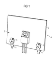
- FIG. 1 shows an example designed as a heat sink component 2 with an electronic component mounted on this.
- the determination of a front 3 and back 4 is chosen to better describe the invention and has no effect on the operation of the invention.
- the first end sections 7 of the two soldering pins 1 protrude beyond the lower edge of the component 2.
- the arrangement is thus suitable to be placed with the lower edge of the component 2 on a printed circuit board, wherein the Lötfahen of the electronic component and beyond the edge of the component 2 protruding first end portions 7 of the solder pins 1 passed through holes in the conductor plate and on the Bottom of the circuit board to be soldered.
- soldering pins 1 are formed by way of example as bent punched parts, wherein depending on the shape and the mass of the component 2 differently many soldering pins 1 are provided to ensure a stable fixation of the component 2 on a printed circuit board. For each solder pin 1, an opening 5 of the component 2 is provided.
- FIG. 2 is a detailed representation of the solder pin 1 used in a breakthrough 5 mapped.
- the component 2 is shown cut to make the contact points of the solder pin 1 with the component 2 visible.
- the FIGS. 3 and 4 show oblique views of the solder pin 1 with the in FIG. 2 illustrated exemplary embodiment.
- the solder pin 1 has a central portion 8 with a rectangular shape, wherein this rectangular central portion 8 extends laterally beyond the front edge of the aperture 5 and is thus supported on the front side of the component 2.
- the middle section 8 also has by way of example a bore 11 which is suitable for soldering in contact wires.
- the middle section 8 of the soldering pin merges via folds into the two end sections 7, 9 of the soldering pin 1.
- the first end portion 7 is connected in this way via a double fold in S-shape with the central portion 8, that the S-shaped portion in the opening 5 is arranged and the first end portion 7 parallel to the central portion 8 extending on the back of the component. 2 is supported.
- the S-shaped portion of the soldering pin 1 is supported on the inner wall of the opening 5, wherein the width of this S-shaped portion corresponds to the width of the opening 5.
- the edge formed by this inner wall and the surface on the rear side of the component 2 is expediently provided with a chamfer 6 in order to release the fold of the soldering pin 1 at this point.
- the first end portion 7 of the soldering pin 1 is in turn subdivided into two sections, wherein a first section for support on the rear side 4 of the component 2 with a constant cross section merges into the S-shaped section.
- a second section is formed as Lötfahne for passage through a printed circuit board and has a smaller cross section.
- the second end portion 9 of the solder pin is connected with a fold to the central portion 8.
- the second End portion 9 in this case again has a smaller width than the middle section 8, so that it is suitable for passage through the opening 5.
- the bending angle is between about 90 ° and about 135 ° to allow the insertion of the solder pin 1 in the opening 5.
- the insertion takes place in such a way that first the first end portion 7 is guided through the opening 5 and that then by a tilting movement over a tilting point at the contact point between the inner wall of the aperture 5 and the S-shaped portion of the soldering pin 1 of the second end portions 9 is guided through the opening 5 until the middle section 8 is supported with its lateral projections on the front side 3 of the component 2. This process is advantageously carried out without tools by hand.
- a projection 10 is provided by way of example.
- This projection 10 causes the second end portion 9 springs during insertion of the solder pin 1 in the opening 5 in the direction of the tilting point. In the end position, the projection 10 engages at the edge of the aperture 5 and fixed in this way the solder pin 1 in this position.
- the second end portion 9 can be supported after the passage through the opening 5 by a new fold on the back 4 of the component 2.
- a simple embodiment of the projection 10 provides that the second end portion 9 of the soldering pin 4 is formed slotted, wherein two legs formed by a slot are interconnected by a connecting web at the end of the second end portion 9. A leg is connected via the fold to the central portion 8 of the solder pin 1.
- the second leg is formed as a projection 10 by a leading away from the first end portion 7 fold.
- the bending angle is between about 10 ° and about 45 °.
- the angle of the thickness of the component 2 and the bending angle between the middle section 8 and the second end section 9 in such a way adapt that on the one hand, the second end portion 9 can be passed through the opening 5 and that on the other hand, a locking of the projection 10 at the rear edge of the opening 5 is possible.
- solder pin 1 formed as a stamped part The electrical contact between a solder pin 1 formed as a stamped part and a component 2 is improved in that the punching burr 12 is pressed into the inner wall of the opening 5.
Landscapes
- Engineering & Computer Science (AREA)
- Manufacturing & Machinery (AREA)
- Microelectronics & Electronic Packaging (AREA)
- Multi-Conductor Connections (AREA)
- Coupling Device And Connection With Printed Circuit (AREA)
Applications Claiming Priority (1)
| Application Number | Priority Date | Filing Date | Title |
|---|---|---|---|
| AT11182007 | 2007-07-17 |
Publications (2)
| Publication Number | Publication Date |
|---|---|
| EP2018091A2 true EP2018091A2 (fr) | 2009-01-21 |
| EP2018091A3 EP2018091A3 (fr) | 2010-05-19 |
Family
ID=40086462
Family Applications (1)
| Application Number | Title | Priority Date | Filing Date |
|---|---|---|---|
| EP08103709A Withdrawn EP2018091A3 (fr) | 2007-07-17 | 2008-04-24 | Composant doté d'un plot à souder |
Country Status (2)
| Country | Link |
|---|---|
| EP (1) | EP2018091A3 (fr) |
| AT (1) | AT10465U1 (fr) |
Cited By (2)
| Publication number | Priority date | Publication date | Assignee | Title |
|---|---|---|---|---|
| CN113015350A (zh) * | 2021-02-18 | 2021-06-22 | 珠海格力智能装备有限公司 | 固定装置 |
| CN116347791A (zh) * | 2023-04-07 | 2023-06-27 | 嘉兴市佳祺电子科技有限公司 | 铝基板与电解电容焊接组装方法 |
Citations (2)
| Publication number | Priority date | Publication date | Assignee | Title |
|---|---|---|---|---|
| US4544942A (en) | 1982-02-22 | 1985-10-01 | Aavid Engineering, Inc. | Heat sinks with staked solderable studs |
| DE69632865T2 (de) | 1995-10-13 | 2005-07-14 | Aavid Thermalloy Llc | Transistor-lötclip und kühlkörper |
Family Cites Families (3)
| Publication number | Priority date | Publication date | Assignee | Title |
|---|---|---|---|---|
| GB798130A (en) * | 1956-01-13 | 1958-07-16 | Emi Ltd | Improvements in or relating to methods of mounting electrical components |
| NL8802678A (nl) * | 1988-11-01 | 1990-06-01 | Du Pont Nederland | Contactelement en contactelementsamenstel van elektrisch geleidend materiaal, in het bijzonder voor oppervlaktemontagetechniek. |
| JP4131724B2 (ja) * | 2004-10-18 | 2008-08-13 | Tdk株式会社 | 回路基板への端子の取付構造 |
-
2008
- 2008-04-24 EP EP08103709A patent/EP2018091A3/fr not_active Withdrawn
- 2008-08-05 AT AT0806308U patent/AT10465U1/de not_active IP Right Cessation
Patent Citations (2)
| Publication number | Priority date | Publication date | Assignee | Title |
|---|---|---|---|---|
| US4544942A (en) | 1982-02-22 | 1985-10-01 | Aavid Engineering, Inc. | Heat sinks with staked solderable studs |
| DE69632865T2 (de) | 1995-10-13 | 2005-07-14 | Aavid Thermalloy Llc | Transistor-lötclip und kühlkörper |
Cited By (2)
| Publication number | Priority date | Publication date | Assignee | Title |
|---|---|---|---|---|
| CN113015350A (zh) * | 2021-02-18 | 2021-06-22 | 珠海格力智能装备有限公司 | 固定装置 |
| CN116347791A (zh) * | 2023-04-07 | 2023-06-27 | 嘉兴市佳祺电子科技有限公司 | 铝基板与电解电容焊接组装方法 |
Also Published As
| Publication number | Publication date |
|---|---|
| EP2018091A3 (fr) | 2010-05-19 |
| AT10465U1 (de) | 2009-03-15 |
Similar Documents
| Publication | Publication Date | Title |
|---|---|---|
| EP1403968B1 (fr) | Borne de raccordement | |
| DE69404215T2 (de) | Halteklammer für einen auf eine Leiterplatte montierten elektrischen Verbinder und Verfahren für die Verwendung | |
| EP1950836B1 (fr) | Borne de connexion électrique | |
| DE10006530A1 (de) | Antennenfeder | |
| WO2017194323A1 (fr) | Pince à ressort, outil de montage, procédé de fixation de partenaires de contact et système de liaison pour la réalisaton d'une liaison électrique et mécanique entre partenaires de contact | |
| DE10153170C1 (de) | Federkraftklemme | |
| WO2008077858A1 (fr) | Support | |
| DE102012016281A1 (de) | Elektrische Verbindungsanordnung und deren Bauteile | |
| WO2020212122A1 (fr) | Borne à ressort et procédé de fabrication d'une borne à ressort | |
| WO1995033291A1 (fr) | Connecteur enfichable monte en surface | |
| DE19726856C1 (de) | Flachstecker für elektrische Steckverbindungen | |
| AT10465U1 (de) | Bauteil mit lötpin | |
| EP1153460A1 (fr) | Dispositif pour assembler electriquement et mecaniquement deux plaquettes a circuit imprime | |
| BE1026101B1 (de) | Kontaktelement mit einem Kontaktkörper und einem daran angeordneten Federelement | |
| DE3828904C2 (fr) | ||
| DE102010043495B4 (de) | Elektrisches Bauteil zur Oberflächenmontage | |
| EP4231459A1 (fr) | Dispositif de raccordement et unité de raccordement | |
| DE10243407B4 (de) | Befestigungsvorrichtung für einen Stecker | |
| DE102022119352A1 (de) | Thermischer Presspassungsanschluss | |
| DE102017121379A1 (de) | Klammerkontakt zum elektrischen kontaktieren von zumindest zwei kontaktelementen | |
| DE102021213350A1 (de) | Kontaktierungsanordnung und Elektronikbaugruppe | |
| WO2002091524A1 (fr) | Connecteur electrique | |
| DE102005061827B4 (de) | Computergehäuse | |
| DE102004027859B4 (de) | Leiterplatte und Leiterplattenvorrichtung | |
| DE10047126A1 (de) | Befestigungseinrichtung |
Legal Events
| Date | Code | Title | Description |
|---|---|---|---|
| PUAI | Public reference made under article 153(3) epc to a published international application that has entered the european phase |
Free format text: ORIGINAL CODE: 0009012 |
|
| AK | Designated contracting states |
Kind code of ref document: A2 Designated state(s): AT BE BG CH CY CZ DE DK EE ES FI FR GB GR HR HU IE IS IT LI LT LU LV MC MT NL NO PL PT RO SE SI SK TR |
|
| AX | Request for extension of the european patent |
Extension state: AL BA MK RS |
|
| RAP1 | Party data changed (applicant data changed or rights of an application transferred) |
Owner name: SIEMENS AKTIENGESELLSCHAFT |
|
| PUAL | Search report despatched |
Free format text: ORIGINAL CODE: 0009013 |
|
| AK | Designated contracting states |
Kind code of ref document: A3 Designated state(s): AT BE BG CH CY CZ DE DK EE ES FI FR GB GR HR HU IE IS IT LI LT LU LV MC MT NL NO PL PT RO SE SI SK TR |
|
| AX | Request for extension of the european patent |
Extension state: AL BA MK RS |
|
| 17P | Request for examination filed |
Effective date: 20101118 |
|
| AKX | Designation fees paid |
Designated state(s): AT BE BG CH CY CZ DE DK EE ES FI FR GB GR HR HU IE IS IT LI LT LU LV MC MT NL NO PL PT RO SE SI SK TR |
|
| RAP1 | Party data changed (applicant data changed or rights of an application transferred) |
Owner name: SIEMENS AKTIENGESELLSCHAFT |
|
| 17Q | First examination report despatched |
Effective date: 20130701 |
|
| STAA | Information on the status of an ep patent application or granted ep patent |
Free format text: STATUS: THE APPLICATION IS DEEMED TO BE WITHDRAWN |
|
| 18D | Application deemed to be withdrawn |
Effective date: 20151103 |