EP2018676B1 - Procédé de production d'un élément multicouche - Google Patents
Procédé de production d'un élément multicouche Download PDFInfo
- Publication number
- EP2018676B1 EP2018676B1 EP07724995A EP07724995A EP2018676B1 EP 2018676 B1 EP2018676 B1 EP 2018676B1 EP 07724995 A EP07724995 A EP 07724995A EP 07724995 A EP07724995 A EP 07724995A EP 2018676 B1 EP2018676 B1 EP 2018676B1
- Authority
- EP
- European Patent Office
- Prior art keywords
- layer
- surface tension
- medium
- dried
- spreading
- Prior art date
- Legal status (The legal status is an assumption and is not a legal conclusion. Google has not performed a legal analysis and makes no representation as to the accuracy of the status listed.)
- Not-in-force
Links
Images
Classifications
-
- H—ELECTRICITY
- H10—SEMICONDUCTOR DEVICES; ELECTRIC SOLID-STATE DEVICES NOT OTHERWISE PROVIDED FOR
- H10K—ORGANIC ELECTRIC SOLID-STATE DEVICES
- H10K71/00—Manufacture or treatment specially adapted for the organic devices covered by this subclass
- H10K71/10—Deposition of organic active material
- H10K71/12—Deposition of organic active material using liquid deposition, e.g. spin coating
-
- B—PERFORMING OPERATIONS; TRANSPORTING
- B05—SPRAYING OR ATOMISING IN GENERAL; APPLYING FLUENT MATERIALS TO SURFACES, IN GENERAL
- B05D—PROCESSES FOR APPLYING FLUENT MATERIALS TO SURFACES, IN GENERAL
- B05D7/00—Processes, other than flocking, specially adapted for applying liquids or other fluent materials to particular surfaces or for applying particular liquids or other fluent materials
- B05D7/50—Multilayers
- B05D7/52—Two layers
- B05D7/54—No clear coat specified
- B05D7/546—No clear coat specified each layer being cured, at least partially, separately
-
- Y—GENERAL TAGGING OF NEW TECHNOLOGICAL DEVELOPMENTS; GENERAL TAGGING OF CROSS-SECTIONAL TECHNOLOGIES SPANNING OVER SEVERAL SECTIONS OF THE IPC; TECHNICAL SUBJECTS COVERED BY FORMER USPC CROSS-REFERENCE ART COLLECTIONS [XRACs] AND DIGESTS
- Y02—TECHNOLOGIES OR APPLICATIONS FOR MITIGATION OR ADAPTATION AGAINST CLIMATE CHANGE
- Y02E—REDUCTION OF GREENHOUSE GAS [GHG] EMISSIONS, RELATED TO ENERGY GENERATION, TRANSMISSION OR DISTRIBUTION
- Y02E10/00—Energy generation through renewable energy sources
- Y02E10/50—Photovoltaic [PV] energy
- Y02E10/549—Organic PV cells
-
- Y—GENERAL TAGGING OF NEW TECHNOLOGICAL DEVELOPMENTS; GENERAL TAGGING OF CROSS-SECTIONAL TECHNOLOGIES SPANNING OVER SEVERAL SECTIONS OF THE IPC; TECHNICAL SUBJECTS COVERED BY FORMER USPC CROSS-REFERENCE ART COLLECTIONS [XRACs] AND DIGESTS
- Y02—TECHNOLOGIES OR APPLICATIONS FOR MITIGATION OR ADAPTATION AGAINST CLIMATE CHANGE
- Y02P—CLIMATE CHANGE MITIGATION TECHNOLOGIES IN THE PRODUCTION OR PROCESSING OF GOODS
- Y02P70/00—Climate change mitigation technologies in the production process for final industrial or consumer products
- Y02P70/50—Manufacturing or production processes characterised by the final manufactured product
Definitions
- the invention relates to a method for producing a multilayer structure consisting of layered media having different surface tensions.
- the application of the layered media which may be lacquers, solutions, etc., may be problematic. These problems are wetting problems when the layered media of the multi-layered structure have substantially different surface tensions from each other.
- a multilayer structure of homogeneous layers, which have the desired properties, are so far only be produced with great difficulty. These properties may be physical properties such as electrical or electronic properties.
- a method for producing a multi-layer coating for example a multi-layer coating, known, in which a first coating, a subsequent coating material is applied and cured.
- the first coating is selected and / or modified in such a way and / or the subsequent coating material is selected such that the quotient of the surface energy of the second coating and the surface energy of the first coating is less than or equal to 1.
- the first coating can be modified there, for example, by means of a primer.
- the active layer has a first and a second charge transfer material.
- the first charge transfer material may be a conductive polymer.
- the second charge transfer material may be an organic material such as a conjugated polymer.
- the invention has for its object to provide a method of the type mentioned, in which it is easily possible to homogeneously arrange layer media with different surface tensions and surface energies to each other to realize a desired multi-layer structure.
- a first layer of a liquid first medium having a first surface tension is applied to a carrier, which is formed by a flexible film, and a second layer of a liquid second medium having a second surface tension is applied to the first layer after drying thereof greater than the first surface tension, and prior to applying the second layer to the dried first layer, a spreading layer is applied, wherein the spreading layer is a metal thin film or a metal nucleation or has capillarity.
- the first and second layers of the multi-layer structure may also be more than two layers.
- Table 2 below shows the surface energies of PET coated with SC and PEDOT / PSS, the determination of the surface energies having been determined by means of the "Optical Contact Angle Measurement Unit OCA 20" from DATA PHYSICS.
- Table 2 substratum (solid state) surface energy (total) (MN / m) SC coated film 26.24 PEDOT / PSS coated film 48.16
- the surface energy of SC coated PET is on the order of 26 mN / m and the surface energy of PEDOT / PSS coated PET is on the order of 48 mN / m.
- the corresponding liquids have a surface tension of approx. 32 mN / m for SC and approx. 46 mN / m for PEDOT / PSS. If, for example, a PET film coated with PEDOT / PSS is to be coated with SC, spreading of the liquid SC medium, ie good wetting of the SC on the PEDOT / PSS, results without further ado.
- a SC coated PET film is to be coated with liquid PEDOT / PSS
- the surface tension of the liquid PEDOT / PSS is greater than the surface energy of the dried SC
- no spreading of the PEDOT / PSS on the SC ie only insufficient wetting of the PEDOT / PSS on the dried SC.
- a spreading layer is applied to the dried SC layer according to the invention.
- the spreading layer may be a metal thin layer.
- the spreading layer is a metal nucleation provided on the dried first layer whose surface energy is smaller than the surface tension of the liquid second medium to be applied to the dried first layer.
- the spreading layer may also have capillarity.
- the metal thin film can be made by vacuum evaporation, sputtering, and the like.
- a germ layer forming the spreading layer can be produced in a galvanic method known per se.
- At least one precoat can be applied to the carrier formed by a flexible film prior to the application of the first layer.
- This at least one pre-layer may be an electrically conductive layer which, for example, forms an electrode of an electrical component such as a solar cell.
- the first and second layers may be organic semiconductor media as exemplified above as SC and PEDOT / PSS. If the said layers consist of organic semiconductor media, polymer solar cells, for example, can be produced according to the invention.
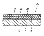
- the figure shows a multilayer structure 10 with a support 12 formed by a flexible film, on which at least one pre-layer 14 is provided.
- a first layer 16 of a applied liquid first medium having a first surface tension On the at least one pre-layer 14 is a first layer 16 of a applied liquid first medium having a first surface tension. After drying, a second layer 18 of a liquid second medium having a second surface tension is applied to the first layer 16.
- the surface energy of the dried first layer 16 is less than the second surface tension of the liquid second medium for the second layer 18, so that a spreading layer 20 is provided on the dried first layer 16 prior to the application of the second layer 18.
- This spreading layer 20 can be a vapor-deposited or cathode-sputtered metal thin layer or a galvanic nucleation or the like.
- the spreading layer 20 may have a certain capillarity to effect reliable wetting of the dried first layer 16 with the liquid medium for the second layer 18.
- a thin metal layer 22 can then be provided on the dried second layer 18, which-like the pre-layer 14 -can form an electrode of a polymer solar cell.
Landscapes
- Engineering & Computer Science (AREA)
- Manufacturing & Machinery (AREA)
- Photovoltaic Devices (AREA)
- Laminated Bodies (AREA)
- Application Of Or Painting With Fluid Materials (AREA)
- Silver Salt Photography Or Processing Solution Therefor (AREA)
- Compounds Of Unknown Constitution (AREA)
- Photosensitive Polymer And Photoresist Processing (AREA)
- Transition And Organic Metals Composition Catalysts For Addition Polymerization (AREA)
Claims (4)
- Procédé de fabrication d'un produit multicouche (10) se composant de milieux stratifiés, qui présentent diverses tensions superficielles et diverses énergies superficielles,
caractérisé en ce
qu'une première couche (16) se composant d'un premier milieu liquide présentant une première tension superficielle est appliquée sur un support (12) formé par une feuille flexible et en ce qu'une deuxième couche (18) se composant d'un second milieu liquide présentant une seconde tension superficielle plus grande que la première tension superficielle est appliquée sur la première couche (16) après le séchage de cette dernière, et en ce qu'une couche de dispersion (20) est appliquée sur la première couche ayant séché (16) avant l'application de la seconde couche (18), la couche de dispersion (20) étant une fine couche métallique ou une couche de nucléation métallique ou possédant une capillarité. - Procédé selon la revendication 1,
caractérisé en ce
qu'au moins une pré-couche (14) est appliquée sur le support (12) avant l'application de la première couche (16). - Procédé selon la revendication 1,
caractérisé en ce
que la première et la seconde couches (16 et 18) se composent de milieux semi-conducteurs organiques. - Utilisation du procédé selon l'une quelconque des revendications 1 à 3 servant à la fabrication de cellules solaires polymères.
Applications Claiming Priority (2)
| Application Number | Priority Date | Filing Date | Title |
|---|---|---|---|
| DE102006021410A DE102006021410B4 (de) | 2006-05-09 | 2006-05-09 | Verfahren zur Herstellung eines Mehrschichtgebildes und Verwendung des Verfahrens |
| PCT/EP2007/004072 WO2007128575A1 (fr) | 2006-05-09 | 2007-05-08 | Procédé de production d'un élément multicouche |
Publications (2)
| Publication Number | Publication Date |
|---|---|
| EP2018676A1 EP2018676A1 (fr) | 2009-01-28 |
| EP2018676B1 true EP2018676B1 (fr) | 2010-05-12 |
Family
ID=38461819
Family Applications (1)
| Application Number | Title | Priority Date | Filing Date |
|---|---|---|---|
| EP07724995A Not-in-force EP2018676B1 (fr) | 2006-05-09 | 2007-05-08 | Procédé de production d'un élément multicouche |
Country Status (9)
| Country | Link |
|---|---|
| US (1) | US20090220681A1 (fr) |
| EP (1) | EP2018676B1 (fr) |
| JP (1) | JP5650907B2 (fr) |
| CN (1) | CN101501879B (fr) |
| AT (1) | ATE467913T1 (fr) |
| DE (2) | DE102006021410B4 (fr) |
| DK (1) | DK2018676T3 (fr) |
| ES (1) | ES2346095T3 (fr) |
| WO (1) | WO2007128575A1 (fr) |
Families Citing this family (3)
| Publication number | Priority date | Publication date | Assignee | Title |
|---|---|---|---|---|
| DE102012105860A1 (de) * | 2012-07-02 | 2015-03-26 | Heliatek Gmbh | Photoaktives organisches Bauelement mit einer optisch transparenten Elektrode und Verfahren zum Herstellen |
| DE102015202149B3 (de) * | 2015-02-06 | 2016-08-11 | Siemens Aktiengesellschaft | Elektrischer Energiespeicher mit effizienter Wärmeabfuhr |
| JP7491863B2 (ja) * | 2021-03-31 | 2024-05-28 | ニチコン株式会社 | 電解コンデンサの製造方法 |
Family Cites Families (18)
| Publication number | Priority date | Publication date | Assignee | Title |
|---|---|---|---|---|
| DE2012063A1 (de) * | 1970-03-13 | 1971-09-30 | Siemens Ag | Verfahren zum Herstellen von aus Alu minium Legierungen bestehenden Kontakt metallschichten an Halbleiterbauelementen |
| DE2540943B2 (de) * | 1975-09-13 | 1978-02-02 | W.C. Heraeus Gmbh, 6450 Hanau | Kontaktkoerper fuer einen elektrischen steckkontakt |
| JPS63290733A (ja) * | 1987-05-22 | 1988-11-28 | Nippei Toyama Corp | 包装用金属化フィルムの加工法 |
| JP2625874B2 (ja) * | 1988-05-11 | 1997-07-02 | 大日本印刷株式会社 | サッシ外装用メタリック化粧シート |
| JP3769842B2 (ja) * | 1996-11-05 | 2006-04-26 | 東レ株式会社 | 金属蒸着フィルム、その製造方法、およびそれを用いたコンデンサ |
| JP2001305321A (ja) * | 2000-04-20 | 2001-10-31 | Toyobo Co Ltd | 面光源用反射フィルム |
| JP2001305313A (ja) * | 2000-04-20 | 2001-10-31 | Toyobo Co Ltd | 面光源用反射フィルム |
| JP4604143B2 (ja) * | 2001-01-24 | 2010-12-22 | トピー工業株式会社 | 表面が光輝化処理された金属または樹脂材料およびその光輝化処理方法 |
| US6946597B2 (en) * | 2002-06-22 | 2005-09-20 | Nanosular, Inc. | Photovoltaic devices fabricated by growth from porous template |
| DE10306357B4 (de) * | 2003-02-15 | 2006-01-12 | Basf Coatings Ag | Verfahren zur Herstellung einer Mehrschichtbeschichtung und dessen Verwendung |
| JP2005019056A (ja) * | 2003-06-24 | 2005-01-20 | Toray Ind Inc | 複合透明導電性基材とそれを用いたディスプレイ |
| US7686978B2 (en) * | 2003-09-24 | 2010-03-30 | E. I. Du Pont De Nemours And Company | Method for the application of active materials onto active surfaces and devices made with such methods |
| US20050067949A1 (en) * | 2003-09-30 | 2005-03-31 | Sriram Natarajan | Solvent mixtures for an organic electronic device |
| WO2005064705A1 (fr) * | 2003-12-22 | 2005-07-14 | Koninklijke Philips Electronics N.V. | Augmentation de la mouillabilite de solutions polymeres a deposer sur des couches en polymeres ferroelectriques hydrophobes |
| AU2005333609A1 (en) * | 2004-10-25 | 2007-01-04 | Hsing-En Elbert Wu | Stacked layer electrode for organic electronic devices |
| KR100658263B1 (ko) * | 2005-09-29 | 2006-12-14 | 삼성전자주식회사 | 적층형 광전변환소자 및 그의 제조방법 |
| US8389174B2 (en) * | 2006-01-27 | 2013-03-05 | GM Global Technology Operations LLC | Super-hydrophilic nanoporous electrically conductive coatings for PEM fuel cells |
| FR2935763B1 (fr) * | 2008-09-09 | 2010-10-08 | Commissariat Energie Atomique | Micropompe pour microfluidique continue |
-
2006
- 2006-05-09 DE DE102006021410A patent/DE102006021410B4/de not_active Expired - Fee Related
-
2007
- 2007-05-08 EP EP07724995A patent/EP2018676B1/fr not_active Not-in-force
- 2007-05-08 JP JP2009508244A patent/JP5650907B2/ja not_active Expired - Fee Related
- 2007-05-08 ES ES07724995T patent/ES2346095T3/es active Active
- 2007-05-08 CN CN2007800209706A patent/CN101501879B/zh not_active Expired - Fee Related
- 2007-05-08 AT AT07724995T patent/ATE467913T1/de active
- 2007-05-08 DK DK07724995.1T patent/DK2018676T3/da active
- 2007-05-08 WO PCT/EP2007/004072 patent/WO2007128575A1/fr not_active Ceased
- 2007-05-08 DE DE502007003744T patent/DE502007003744D1/de active Active
- 2007-05-08 US US12/227,099 patent/US20090220681A1/en not_active Abandoned
Also Published As
| Publication number | Publication date |
|---|---|
| ATE467913T1 (de) | 2010-05-15 |
| EP2018676A1 (fr) | 2009-01-28 |
| US20090220681A1 (en) | 2009-09-03 |
| ES2346095T3 (es) | 2010-10-08 |
| WO2007128575A1 (fr) | 2007-11-15 |
| JP5650907B2 (ja) | 2015-01-07 |
| DK2018676T3 (da) | 2010-09-13 |
| JP2009536110A (ja) | 2009-10-08 |
| DE102006021410A1 (de) | 2007-11-15 |
| DE502007003744D1 (de) | 2010-06-24 |
| CN101501879B (zh) | 2012-02-01 |
| CN101501879A (zh) | 2009-08-05 |
| DE102006021410B4 (de) | 2009-07-16 |
Similar Documents
| Publication | Publication Date | Title |
|---|---|---|
| DE102010048031A1 (de) | Polythiophene beinhaltende Dispersionen mit definiertem Sulfat-Gehalt | |
| EP2018676B1 (fr) | Procédé de production d'un élément multicouche | |
| DE112018000321T5 (de) | Folienkondensator, verfahren zum herstellen eines folienkondensators,dielektrische harzfolie und verfahren zum herstellen einer dielektrischen harzfolie | |
| DE102004036793A1 (de) | Nanoporöse Fullerenschichten und deren Verwendung in der organischen Photovoltaik | |
| DE102015225701A1 (de) | Kollektorelektroden-Schutzschicht für Farbstoff-sensibilisierte Solarzellen und Verfahren zu deren Bildung | |
| DE112011103939T5 (de) | Elektronische Vorrichtungen | |
| DE102014202945B4 (de) | Verfahren zum Herstellen eines organischen elektronischen Bauelementes und organisches elektronisches Bauelement | |
| DE102014200443B4 (de) | Sensorelement zur Bestimmung von Dehnungen | |
| WO2003107454A2 (fr) | Materiau destine a une couche fonctionnelle mince et faiblement conductrice pour une oled et procede de fabrication | |
| WO2005001923A2 (fr) | Solution et procede de traitement d'un substrat et composant a semi-conducteur | |
| DE102007034252A1 (de) | Modul und Verfahren zu seiner Herstellung | |
| EP0554798A2 (fr) | Enduit pour feuilles plastiques | |
| EP1514318A2 (fr) | Materiau pour couche fonctionnelle d'un composant electronique organique, procede de production et utilisation correspondants | |
| DE102012202262B4 (de) | Verfahren zur Herstellung eines Festelektrolyten umfassend eine poröse Dünnschicht, ein Festelektrolyt und eine Farbstoffsolarzelle, die diesen umfassst. | |
| DE102006033887B4 (de) | Verfahren zur Herstellung eines Mehrschichtkörpers mit leitfähiger Polymerschicht | |
| CN106674571A (zh) | 一种透明导电膜 | |
| EP2995703A1 (fr) | Procédé de fabrication d'électrodes de dérivation de surface et semi-produit destiné à exécuter le procédé | |
| EP2183797B1 (fr) | Couche de passivation pour une couche d'oxyde conductrice transparente dans un élément doté d'une couche active organique | |
| EP2027615A1 (fr) | Composant avec une couche structurée sur un substrat porteur | |
| DE102023211658A1 (de) | Wässrige, leitfähige, druckbare Ruß-gefüllte Tinte, Verfahren zu deren Herstellung, beschichteter Gegenstand sowie Verfahren zur Herstellung des be-schichteten Gegenstands | |
| DE112017005605T5 (de) | Artikel und Substrate, die eine verbesserte Leistungsfähigkeit durckbarer Elektronik bereitstellen | |
| DE102008003251A1 (de) | Verfahren zur Herstellung von erhöhte Leitfähigkeit aufweisenden Beschichtungen auf Basis von Polythiophen und dessen Derivaten | |
| WO2008012081A1 (fr) | Procédé d'impression pour produire un composant électrique organique | |
| DE102008059389A1 (de) | Verfahren zur Herstellung von erhöhte Leitfähigkeit aufweisenden Beschichtungen auf Basis von Polythiophen und dessen Derivaten | |
| DE102013225904A1 (de) | Beschichtungsmittel zum Herstellen einer elektrisch leitfähigen Schicht |
Legal Events
| Date | Code | Title | Description |
|---|---|---|---|
| PUAI | Public reference made under article 153(3) epc to a published international application that has entered the european phase |
Free format text: ORIGINAL CODE: 0009012 |
|
| 17P | Request for examination filed |
Effective date: 20081104 |
|
| AK | Designated contracting states |
Kind code of ref document: A1 Designated state(s): AT BE BG CH CY CZ DE DK EE ES FI FR GB GR HU IE IS IT LI LT LU LV MC MT NL PL PT RO SE SI SK TR |
|
| AX | Request for extension of the european patent |
Extension state: AL BA HR MK RS |
|
| GRAP | Despatch of communication of intention to grant a patent |
Free format text: ORIGINAL CODE: EPIDOSNIGR1 |
|
| DAX | Request for extension of the european patent (deleted) | ||
| GRAS | Grant fee paid |
Free format text: ORIGINAL CODE: EPIDOSNIGR3 |
|
| GRAA | (expected) grant |
Free format text: ORIGINAL CODE: 0009210 |
|
| AK | Designated contracting states |
Kind code of ref document: B1 Designated state(s): AT BE BG CH CY CZ DE DK EE ES FI FR GB GR HU IE IS IT LI LT LU LV MC MT NL PL PT RO SE SI SK TR |
|
| REG | Reference to a national code |
Ref country code: GB Ref legal event code: FG4D Free format text: NOT ENGLISH |
|
| REG | Reference to a national code |
Ref country code: CH Ref legal event code: EP |
|
| REG | Reference to a national code |
Ref country code: IE Ref legal event code: FG4D Free format text: LANGUAGE OF EP DOCUMENT: GERMAN |
|
| REF | Corresponds to: |
Ref document number: 502007003744 Country of ref document: DE Date of ref document: 20100624 Kind code of ref document: P |
|
| REG | Reference to a national code |
Ref country code: NL Ref legal event code: VDEP Effective date: 20100512 |
|
| REG | Reference to a national code |
Ref country code: DK Ref legal event code: T3 |
|
| REG | Reference to a national code |
Ref country code: ES Ref legal event code: FG2A Ref document number: 2346095 Country of ref document: ES Kind code of ref document: T3 |
|
| LTIE | Lt: invalidation of european patent or patent extension |
Effective date: 20100512 |
|
| PG25 | Lapsed in a contracting state [announced via postgrant information from national office to epo] |
Ref country code: LT Free format text: LAPSE BECAUSE OF FAILURE TO SUBMIT A TRANSLATION OF THE DESCRIPTION OR TO PAY THE FEE WITHIN THE PRESCRIBED TIME-LIMIT Effective date: 20100512 Ref country code: SE Free format text: LAPSE BECAUSE OF FAILURE TO SUBMIT A TRANSLATION OF THE DESCRIPTION OR TO PAY THE FEE WITHIN THE PRESCRIBED TIME-LIMIT Effective date: 20100512 Ref country code: NL Free format text: LAPSE BECAUSE OF FAILURE TO SUBMIT A TRANSLATION OF THE DESCRIPTION OR TO PAY THE FEE WITHIN THE PRESCRIBED TIME-LIMIT Effective date: 20100512 |
|
| PG25 | Lapsed in a contracting state [announced via postgrant information from national office to epo] |
Ref country code: SI Free format text: LAPSE BECAUSE OF FAILURE TO SUBMIT A TRANSLATION OF THE DESCRIPTION OR TO PAY THE FEE WITHIN THE PRESCRIBED TIME-LIMIT Effective date: 20100512 Ref country code: LV Free format text: LAPSE BECAUSE OF FAILURE TO SUBMIT A TRANSLATION OF THE DESCRIPTION OR TO PAY THE FEE WITHIN THE PRESCRIBED TIME-LIMIT Effective date: 20100512 Ref country code: IS Free format text: LAPSE BECAUSE OF FAILURE TO SUBMIT A TRANSLATION OF THE DESCRIPTION OR TO PAY THE FEE WITHIN THE PRESCRIBED TIME-LIMIT Effective date: 20100912 Ref country code: FI Free format text: LAPSE BECAUSE OF FAILURE TO SUBMIT A TRANSLATION OF THE DESCRIPTION OR TO PAY THE FEE WITHIN THE PRESCRIBED TIME-LIMIT Effective date: 20100512 |
|
| REG | Reference to a national code |
Ref country code: IE Ref legal event code: FD4D |
|
| PG25 | Lapsed in a contracting state [announced via postgrant information from national office to epo] |
Ref country code: PL Free format text: LAPSE BECAUSE OF FAILURE TO SUBMIT A TRANSLATION OF THE DESCRIPTION OR TO PAY THE FEE WITHIN THE PRESCRIBED TIME-LIMIT Effective date: 20100512 Ref country code: CY Free format text: LAPSE BECAUSE OF FAILURE TO SUBMIT A TRANSLATION OF THE DESCRIPTION OR TO PAY THE FEE WITHIN THE PRESCRIBED TIME-LIMIT Effective date: 20100609 |
|
| PG25 | Lapsed in a contracting state [announced via postgrant information from national office to epo] |
Ref country code: IE Free format text: LAPSE BECAUSE OF FAILURE TO SUBMIT A TRANSLATION OF THE DESCRIPTION OR TO PAY THE FEE WITHIN THE PRESCRIBED TIME-LIMIT Effective date: 20100512 Ref country code: EE Free format text: LAPSE BECAUSE OF FAILURE TO SUBMIT A TRANSLATION OF THE DESCRIPTION OR TO PAY THE FEE WITHIN THE PRESCRIBED TIME-LIMIT Effective date: 20100512 Ref country code: PT Free format text: LAPSE BECAUSE OF FAILURE TO SUBMIT A TRANSLATION OF THE DESCRIPTION OR TO PAY THE FEE WITHIN THE PRESCRIBED TIME-LIMIT Effective date: 20100913 |
|
| PG25 | Lapsed in a contracting state [announced via postgrant information from national office to epo] |
Ref country code: RO Free format text: LAPSE BECAUSE OF FAILURE TO SUBMIT A TRANSLATION OF THE DESCRIPTION OR TO PAY THE FEE WITHIN THE PRESCRIBED TIME-LIMIT Effective date: 20100512 Ref country code: CZ Free format text: LAPSE BECAUSE OF FAILURE TO SUBMIT A TRANSLATION OF THE DESCRIPTION OR TO PAY THE FEE WITHIN THE PRESCRIBED TIME-LIMIT Effective date: 20100512 Ref country code: SK Free format text: LAPSE BECAUSE OF FAILURE TO SUBMIT A TRANSLATION OF THE DESCRIPTION OR TO PAY THE FEE WITHIN THE PRESCRIBED TIME-LIMIT Effective date: 20100512 |
|
| PLBE | No opposition filed within time limit |
Free format text: ORIGINAL CODE: 0009261 |
|
| STAA | Information on the status of an ep patent application or granted ep patent |
Free format text: STATUS: NO OPPOSITION FILED WITHIN TIME LIMIT |
|
| 26N | No opposition filed |
Effective date: 20110215 |
|
| PG25 | Lapsed in a contracting state [announced via postgrant information from national office to epo] |
Ref country code: GR Free format text: LAPSE BECAUSE OF FAILURE TO SUBMIT A TRANSLATION OF THE DESCRIPTION OR TO PAY THE FEE WITHIN THE PRESCRIBED TIME-LIMIT Effective date: 20100813 |
|
| REG | Reference to a national code |
Ref country code: DE Ref legal event code: R097 Ref document number: 502007003744 Country of ref document: DE Effective date: 20110214 |
|
| BERE | Be: lapsed |
Owner name: LEONHARD KURZ STIFTUNG & CO. K.G. Effective date: 20110531 Owner name: KONARKA TECHNOLOGIES, INC. Effective date: 20110531 |
|
| PG25 | Lapsed in a contracting state [announced via postgrant information from national office to epo] |
Ref country code: MT Free format text: LAPSE BECAUSE OF FAILURE TO SUBMIT A TRANSLATION OF THE DESCRIPTION OR TO PAY THE FEE WITHIN THE PRESCRIBED TIME-LIMIT Effective date: 20100512 Ref country code: MC Free format text: LAPSE BECAUSE OF NON-PAYMENT OF DUE FEES Effective date: 20110531 |
|
| REG | Reference to a national code |
Ref country code: CH Ref legal event code: PL |
|
| PG25 | Lapsed in a contracting state [announced via postgrant information from national office to epo] |
Ref country code: CH Free format text: LAPSE BECAUSE OF NON-PAYMENT OF DUE FEES Effective date: 20110531 Ref country code: LI Free format text: LAPSE BECAUSE OF NON-PAYMENT OF DUE FEES Effective date: 20110531 |
|
| PG25 | Lapsed in a contracting state [announced via postgrant information from national office to epo] |
Ref country code: BE Free format text: LAPSE BECAUSE OF NON-PAYMENT OF DUE FEES Effective date: 20110531 |
|
| PGFP | Annual fee paid to national office [announced via postgrant information from national office to epo] |
Ref country code: IT Payment date: 20120523 Year of fee payment: 6 |
|
| PGFP | Annual fee paid to national office [announced via postgrant information from national office to epo] |
Ref country code: ES Payment date: 20120525 Year of fee payment: 6 |
|
| REG | Reference to a national code |
Ref country code: DE Ref legal event code: R082 Ref document number: 502007003744 Country of ref document: DE Representative=s name: LOUIS, POEHLAU, LOHRENTZ, DE |
|
| REG | Reference to a national code |
Ref country code: DE Ref legal event code: R082 Ref document number: 502007003744 Country of ref document: DE Representative=s name: LOUIS, POEHLAU, LOHRENTZ, DE Effective date: 20130107 Ref country code: DE Ref legal event code: R081 Ref document number: 502007003744 Country of ref document: DE Owner name: MERCK PATENT GMBH, DE Free format text: FORMER OWNER: KONARKA TECHNOLOGIES, INC., LEONHARD KURZ STIFTUNG & CO. KG, , US Effective date: 20130107 Ref country code: DE Ref legal event code: R081 Ref document number: 502007003744 Country of ref document: DE Owner name: LEONHARD KURZ STIFTUNG & CO. KG, DE Free format text: FORMER OWNER: KONARKA TECHNOLOGIES, INC., LEONHARD KURZ STIFTUNG & CO. KG, , US Effective date: 20130107 Ref country code: DE Ref legal event code: R081 Ref document number: 502007003744 Country of ref document: DE Owner name: MERCK PATENT GMBH, DE Free format text: FORMER OWNERS: KONARKA TECHNOLOGIES, INC., LOWELL, MASS., US; LEONHARD KURZ STIFTUNG & CO. KG, 90763 FUERTH, DE Effective date: 20130107 Ref country code: DE Ref legal event code: R081 Ref document number: 502007003744 Country of ref document: DE Owner name: LEONHARD KURZ STIFTUNG & CO. KG, DE Free format text: FORMER OWNERS: KONARKA TECHNOLOGIES, INC., LOWELL, MASS., US; LEONHARD KURZ STIFTUNG & CO. KG, 90763 FUERTH, DE Effective date: 20130107 |
|
| REG | Reference to a national code |
Ref country code: FR Ref legal event code: TQ Owner name: LEONHARD KURZ STIFTUNG & CO. KG, DE Effective date: 20130308 Ref country code: FR Ref legal event code: TQ Owner name: MERCK KGAA, DE Effective date: 20130308 |
|
| PG25 | Lapsed in a contracting state [announced via postgrant information from national office to epo] |
Ref country code: LU Free format text: LAPSE BECAUSE OF NON-PAYMENT OF DUE FEES Effective date: 20110508 |
|
| REG | Reference to a national code |
Ref country code: FR Ref legal event code: TQ Owner name: LEONHARD KURZ STIFTUNG & CO. KG, DE Effective date: 20130606 Ref country code: FR Ref legal event code: TQ Owner name: MERCK PATENT GMBH, DE Effective date: 20130606 |
|
| REG | Reference to a national code |
Ref country code: GB Ref legal event code: 732E Free format text: REGISTERED BETWEEN 20130711 AND 20130717 |
|
| PG25 | Lapsed in a contracting state [announced via postgrant information from national office to epo] |
Ref country code: TR Free format text: LAPSE BECAUSE OF FAILURE TO SUBMIT A TRANSLATION OF THE DESCRIPTION OR TO PAY THE FEE WITHIN THE PRESCRIBED TIME-LIMIT Effective date: 20100512 Ref country code: BG Free format text: LAPSE BECAUSE OF FAILURE TO SUBMIT A TRANSLATION OF THE DESCRIPTION OR TO PAY THE FEE WITHIN THE PRESCRIBED TIME-LIMIT Effective date: 20100812 |
|
| PG25 | Lapsed in a contracting state [announced via postgrant information from national office to epo] |
Ref country code: HU Free format text: LAPSE BECAUSE OF FAILURE TO SUBMIT A TRANSLATION OF THE DESCRIPTION OR TO PAY THE FEE WITHIN THE PRESCRIBED TIME-LIMIT Effective date: 20100512 |
|
| PG25 | Lapsed in a contracting state [announced via postgrant information from national office to epo] |
Ref country code: IT Free format text: LAPSE BECAUSE OF NON-PAYMENT OF DUE FEES Effective date: 20130508 |
|
| REG | Reference to a national code |
Ref country code: ES Ref legal event code: FD2A Effective date: 20140612 |
|
| PG25 | Lapsed in a contracting state [announced via postgrant information from national office to epo] |
Ref country code: ES Free format text: LAPSE BECAUSE OF NON-PAYMENT OF DUE FEES Effective date: 20130509 |
|
| REG | Reference to a national code |
Ref country code: FR Ref legal event code: PLFP Year of fee payment: 10 |
|
| REG | Reference to a national code |
Ref country code: FR Ref legal event code: PLFP Year of fee payment: 11 |
|
| PGFP | Annual fee paid to national office [announced via postgrant information from national office to epo] |
Ref country code: FR Payment date: 20170522 Year of fee payment: 11 Ref country code: DK Payment date: 20170524 Year of fee payment: 11 Ref country code: DE Payment date: 20170520 Year of fee payment: 11 Ref country code: GB Payment date: 20170524 Year of fee payment: 11 |
|
| PGFP | Annual fee paid to national office [announced via postgrant information from national office to epo] |
Ref country code: AT Payment date: 20170519 Year of fee payment: 11 |
|
| REG | Reference to a national code |
Ref country code: DE Ref legal event code: R119 Ref document number: 502007003744 Country of ref document: DE |
|
| REG | Reference to a national code |
Ref country code: DK Ref legal event code: EBP Effective date: 20180531 |
|
| REG | Reference to a national code |
Ref country code: AT Ref legal event code: MM01 Ref document number: 467913 Country of ref document: AT Kind code of ref document: T Effective date: 20180508 |
|
| GBPC | Gb: european patent ceased through non-payment of renewal fee |
Effective date: 20180508 |
|
| PG25 | Lapsed in a contracting state [announced via postgrant information from national office to epo] |
Ref country code: AT Free format text: LAPSE BECAUSE OF NON-PAYMENT OF DUE FEES Effective date: 20180508 |
|
| PG25 | Lapsed in a contracting state [announced via postgrant information from national office to epo] |
Ref country code: GB Free format text: LAPSE BECAUSE OF NON-PAYMENT OF DUE FEES Effective date: 20180508 Ref country code: DE Free format text: LAPSE BECAUSE OF NON-PAYMENT OF DUE FEES Effective date: 20181201 Ref country code: FR Free format text: LAPSE BECAUSE OF NON-PAYMENT OF DUE FEES Effective date: 20180531 |
|
| PG25 | Lapsed in a contracting state [announced via postgrant information from national office to epo] |
Ref country code: DK Free format text: LAPSE BECAUSE OF NON-PAYMENT OF DUE FEES Effective date: 20180531 |