EP2019301A1 - Elektromagnetische Strahlensonde und Herstellungsverfahren einer solchen Sonde - Google Patents
Elektromagnetische Strahlensonde und Herstellungsverfahren einer solchen Sonde Download PDFInfo
- Publication number
- EP2019301A1 EP2019301A1 EP08305392A EP08305392A EP2019301A1 EP 2019301 A1 EP2019301 A1 EP 2019301A1 EP 08305392 A EP08305392 A EP 08305392A EP 08305392 A EP08305392 A EP 08305392A EP 2019301 A1 EP2019301 A1 EP 2019301A1
- Authority
- EP
- European Patent Office
- Prior art keywords
- membrane
- substrate
- detector
- electromagnetic radiation
- distance
- Prior art date
- Legal status (The legal status is an assumption and is not a legal conclusion. Google has not performed a legal analysis and makes no representation as to the accuracy of the status listed.)
- Granted
Links
- 230000005670 electromagnetic radiation Effects 0.000 title claims abstract description 15
- 238000004519 manufacturing process Methods 0.000 title claims description 10
- 239000012528 membrane Substances 0.000 claims abstract description 75
- 239000000758 substrate Substances 0.000 claims abstract description 61
- 230000005855 radiation Effects 0.000 claims abstract description 17
- 230000006335 response to radiation Effects 0.000 claims abstract 2
- 230000004044 response Effects 0.000 claims description 33
- 239000000463 material Substances 0.000 claims description 8
- 230000003252 repetitive effect Effects 0.000 claims description 2
- 238000001514 detection method Methods 0.000 abstract description 20
- 238000002161 passivation Methods 0.000 description 17
- 238000010276 construction Methods 0.000 description 7
- 230000000694 effects Effects 0.000 description 6
- 230000035945 sensitivity Effects 0.000 description 6
- 238000000034 method Methods 0.000 description 5
- 229910021417 amorphous silicon Inorganic materials 0.000 description 4
- 230000015572 biosynthetic process Effects 0.000 description 4
- 239000006185 dispersion Substances 0.000 description 4
- 239000011159 matrix material Substances 0.000 description 4
- 229910001935 vanadium oxide Inorganic materials 0.000 description 4
- 238000010521 absorption reaction Methods 0.000 description 3
- 229910052751 metal Inorganic materials 0.000 description 3
- 239000002184 metal Substances 0.000 description 3
- 238000001228 spectrum Methods 0.000 description 3
- XHCLAFWTIXFWPH-UHFFFAOYSA-N [O-2].[O-2].[O-2].[O-2].[O-2].[V+5].[V+5] Chemical compound [O-2].[O-2].[O-2].[O-2].[O-2].[V+5].[V+5] XHCLAFWTIXFWPH-UHFFFAOYSA-N 0.000 description 2
- 230000008021 deposition Effects 0.000 description 2
- 239000003989 dielectric material Substances 0.000 description 2
- 238000005530 etching Methods 0.000 description 2
- 238000003384 imaging method Methods 0.000 description 2
- 229910044991 metal oxide Inorganic materials 0.000 description 2
- 150000004706 metal oxides Chemical class 0.000 description 2
- 238000002310 reflectometry Methods 0.000 description 2
- 239000000725 suspension Substances 0.000 description 2
- 238000004616 Pyrometry Methods 0.000 description 1
- 229910052581 Si3N4 Inorganic materials 0.000 description 1
- VYPSYNLAJGMNEJ-UHFFFAOYSA-N Silicium dioxide Chemical compound O=[Si]=O VYPSYNLAJGMNEJ-UHFFFAOYSA-N 0.000 description 1
- XUIMIQQOPSSXEZ-UHFFFAOYSA-N Silicon Chemical compound [Si] XUIMIQQOPSSXEZ-UHFFFAOYSA-N 0.000 description 1
- 230000002745 absorbent Effects 0.000 description 1
- 239000002250 absorbent Substances 0.000 description 1
- 230000015556 catabolic process Effects 0.000 description 1
- 238000006731 degradation reaction Methods 0.000 description 1
- 230000001627 detrimental effect Effects 0.000 description 1
- 239000003344 environmental pollutant Substances 0.000 description 1
- 230000002349 favourable effect Effects 0.000 description 1
- 230000004907 flux Effects 0.000 description 1
- 238000010438 heat treatment Methods 0.000 description 1
- 238000003331 infrared imaging Methods 0.000 description 1
- 231100000719 pollutant Toxicity 0.000 description 1
- 238000011896 sensitive detection Methods 0.000 description 1
- 229910052710 silicon Inorganic materials 0.000 description 1
- 239000010703 silicon Substances 0.000 description 1
- HQVNEWCFYHHQES-UHFFFAOYSA-N silicon nitride Chemical compound N12[Si]34N5[Si]62N3[Si]51N64 HQVNEWCFYHHQES-UHFFFAOYSA-N 0.000 description 1
- 229910052814 silicon oxide Inorganic materials 0.000 description 1
- 230000003595 spectral effect Effects 0.000 description 1
- 230000003313 weakening effect Effects 0.000 description 1
Images


Classifications
-
- G—PHYSICS
- G01—MEASURING; TESTING
- G01J—MEASUREMENT OF INTENSITY, VELOCITY, SPECTRAL CONTENT, POLARISATION, PHASE OR PULSE CHARACTERISTICS OF INFRARED, VISIBLE OR ULTRAVIOLET LIGHT; COLORIMETRY; RADIATION PYROMETRY
- G01J5/00—Radiation pyrometry, e.g. infrared or optical thermometry
- G01J5/10—Radiation pyrometry, e.g. infrared or optical thermometry using electric radiation detectors
- G01J5/20—Radiation pyrometry, e.g. infrared or optical thermometry using electric radiation detectors using resistors, thermistors or semiconductors sensitive to radiation, e.g. photoconductive devices
-
- H—ELECTRICITY
- H10—SEMICONDUCTOR DEVICES; ELECTRIC SOLID-STATE DEVICES NOT OTHERWISE PROVIDED FOR
- H10F—INORGANIC SEMICONDUCTOR DEVICES SENSITIVE TO INFRARED RADIATION, LIGHT, ELECTROMAGNETIC RADIATION OF SHORTER WAVELENGTH OR CORPUSCULAR RADIATION
- H10F39/00—Integrated devices, or assemblies of multiple devices, comprising at least one element covered by group H10F30/00, e.g. radiation detectors comprising photodiode arrays
- H10F39/10—Integrated devices
- H10F39/12—Image sensors
- H10F39/18—Complementary metal-oxide-semiconductor [CMOS] image sensors; Photodiode array image sensors
- H10F39/184—Infrared image sensors
Definitions
- the present invention relates to the field of imaging. It particularly concerns the field of infrared imaging and bolometric pyrometry.
- the present invention relates to a detector comprising a reflective substrate and at least one detection element comprising a membrane sensitive to electromagnetic radiation, suspended above the substrate.
- Bolometric detectors belong to a class of detectors comprising a matrix arrangement of suspended membrane unitary sensing elements. Each of these unitary elements comprises a membrane, rendered absorbent to electromagnetic radiation in a predetermined range of wavelengths and held in suspension over a reflective substrate using resistive thermal structures. , which allow its heating under the effect of radiation and its electrical connection to the substrate.
- substrate is meant here the physical component located directly below the membrane.
- the substrate comprises a so-called “construction” substrate, in which an electronic reading circuit, a passivation layer covering the construction substrate and a reflective layer covering the passivation layer are produced.
- the membrane comprises a bolometric material, that is to say a material whose resistivity varies with the temperature thereof.
- the resistivity variation of the bolometric material under the effect of a temperature variation is then detected by the electronic reading circuit made on the substrate.
- the membrane and the substrate are generally substantially in planar form, and are arranged parallel to each other at a predetermined distance so as to form a quarter wave plate therebetween.
- This quarter wave plate has the effect of optimizing by a resonance phenomenon the response of the detector in the range of wavelengths of interest.
- a bolometric detector for observing a thermal infrared radiation at ambient temperature, that is to say a radiation having a wavelength of between 8 and 14 micrometers
- the distance between the membrane and the substrate is adjusted to about 2.5 micrometers.
- the response also has secondary peaks corresponding to higher interference orders.
- a narrow but high amplitude secondary peak is observed at around 2.5 micrometers, as can be seen in the above-mentioned curve A of FIG. figure 1 .
- the detected wavelength range is restricted due to the fact that the secondary peak (s) are narrow and the detector response between the peaks too low for proper operation.
- a first approach to increase the detection range of this type of sensor is to use two types of detection structures juxtaposed or superimposed, each of these structures being sensitive to a given range of wavelengths.
- This type of detector is complex to manufacture, especially in the case of superimposed structures.
- such detectors necessarily have a reduced resolution because it is necessary to provide twice as many sensitive elements per unit area.
- a second approach to increase the detection range is to use the presence of secondary peaks in the sensor response.
- This approach is however difficult to implement, in particular considering the case where the user focuses for example on a specific wavelength (typically the case of the detection of atmospheric pollutants), this wavelength can be located on the flanks of a peak of sensitivity, in which case low distortions of the sensitivity spectrum from one sensitive point to the other in the same matrix detector, and between different detectors (problem of the detector manufacturer), lead to large signal variations at this wavelength.
- the dispersion is usually very high.
- the detector is from this point of view very precise.
- the response of the detector off the main peak and the secondary peak is generally low.
- the operation of the detector in ranges of wavelengths distant from the peaks is then difficult or impossible.
- the object of the present invention is to solve the aforementioned problems by proposing a detector of the aforementioned type having a wide range of exploitable detection, and which also proves simple to manufacture.
- the subject of the invention is a detector comprising a reflective substrate and at least one detection element comprising a membrane sensitive to radiation suspended above the substrate.
- the distance separating the membrane from the at least one detection element and the substrate is variable, said distance having a predetermined spatial distribution able to minimize rapid variations of a detector response to the radiation in at least a predetermined range of wavelengths
- the variation of the distance between the membrane and the substrate thus makes it possible to modulate the shape of a secondary peak of the curve representative of the response of the detector as a function of the wavelength of the detected radiation, and in particular its gradient and amplitude. , without it being necessary for this to provide a resonance cavity specifically dedicated to the range of wavelengths corresponding to this peak.
- the substrate and / or the suspended membrane have three-dimensional patterns.
- the membrane and the substrate may be substantially parallel in pieces.
- the distance between the suspended membrane and the substrate is distributed between at least a first and a second predetermined value.
- the area areas corresponding to different distance values between the membrane and the substrate may be the same or different.
- the suspended membrane comprises a bolometric material sensitive to a temperature variation resulting from exposure to infrared radiation, the membrane constituting it being able to be sensitive to wavelengths between about 3 microns and about 14 microns.
- the first and second distance values separating the suspended membrane from the substrate are substantially equal to 3 and 2 microns respectively.
- the ratio between the surface of the membrane separated from the substrate by the first distance and the area of the membrane separated from the substrate by the second distance is between about 35 and about 50 percent.
- the three-dimensional patterns made on the membrane and / or on the substrate are repetitive, their repetition pitch being less than or equal to 4 micrometers in the particular case of the preceding configuration.
- the present invention also relates to a method for manufacturing a detector, of the type comprising a step of forming a reflective substrate and a membrane constituting at least one radiation sensitive detection element, and a step suspending the membrane above the substrate.
- the step of forming the substrate and the membrane comprises a step of creating three-dimensional patterns in the substrate and / or the membrane, so as to have a predetermined spatial distribution able to minimize rapid variations of a detector response to the radiation in at least a predetermined range of wavelengths.
- a bolometric detector according to the invention, dedicated to the detection of thermal infrared and means.
- This detector comprises a substantially planar construction substrate 10 in which an electronic reading circuit (not shown), well known per se, is made.
- This detector also comprises a passivation layer 12 covering the construction substrate 10, of a thickness of 1 to a few micrometers, and made of a dielectric material.
- the passivation layer 12 is optionally covered with an additional layer (not shown) of dielectric material, such as a silicon oxide, a silicon nitride or a mixed material, for example silicon oxynitride.
- the passivation of the electronic circuits is traditionally formed, for various reasons, of several layers that should generally not be modified during a subsequent process of forming cavities, otherwise there is a risk of changing their passivity, at least locally.
- the addition of the additional layer which is compatible with the underlying passivation layers, makes it possible to form a texturing by etching, without modifying the characteristics of the reading circuit.
- the detector comprises a plurality of identical elementary bolometric membranes 16, 18, 20, regularly arranged in matrix form, for example with a repetition pitch of between 25 and 40 microns.
- These membranes 16, 18, 20 are substantially flat and are suspended above the reflective layer 14 by means of suspension arms 22-26.
- Each membrane 16, 18, 20 has a small thickness, a few tenths of a micrometer, and comprises a bolometric material, such as for example amorphous silicon (a-Si), vanadium oxide (VOx) or metal oxide (Ti).
- a-Si amorphous silicon
- VOx vanadium oxide
- Ti metal oxide
- the membrane 16, 18, 20 further has a high absorption power at wavelengths between about 3 micrometers and about 14 micrometers.
- the absorption power of the membrane 16, 18, 20 is, in this range, substantially independent at the first order of the wavelength of the incident radiation.
- the membrane comprises a metal layer (not shown), whose layer resistance is between about 300 Ohm per square and about 400 Ohm per square.
- the membrane is for example of the type described in the document FR 2,796,148
- the arrangement of the construction substrate 10, the passivation layer 12, the reflective layer 14 and a membrane 16, 18, 20 constitutes a unitary sensing element of a matrix arrangement of the detector, as is known per se. .
- the reflective layer 14 returns towards the absorbing membrane 16, 18, 20 an infrared flux having passed therethrough without having been absorbed, thereby increasing the overall absorption capacity of the detector by a resonance phenomenon.
- the passivation layer 12 comprises stepped three-dimensional patterns 30, 32, with surfaces parallel to the membranes 16, 18, 20, formed on the surface of the passivation layer 12 facing the membranes 16, 18, 20 and covered by the metallic reflective layer 14.
- These three-dimensional staggered patterns 30, 32 are regularly distributed at a distance D1 and a distance D2 from the membranes 16, 18, 20.
- the distances D1 and D2 are substantially equal to 3 and 2 microns respectively.
- the surface ratio between the separate patterns of the membranes of the distance D1 and the separate patterns of the membranes 16, 18, 20 of the distance D2 is chosen to be substantially equal to 40%. This proportion represents a favorable case in this particular example of description, but in no way constitutes a preferential typical proportion.
- a cavity defined by the membrane 16, 18, 20 of a unitary sensitive element and the three - dimensional patterns 32 separated from the distance D1 form a quarter-wave plate for the wavelength 3 microns.
- the response of the sensitive element is amplified for a range of wavelengths between substantially 8 and substantially 14 micrometers.
- a cavity defined by the membrane and the three-dimensional patterns 30 separated from the distance D2 forms a quarter-wave plate for the wavelength of 2 micrometers.
- the response of the sensitive element is amplified for a range of wavelengths between substantially 6 and substantially 12 micrometers.
- the distance between the membrane 16, 18, 20 of the element and the metal reflective layer 14 is variable. This internal variability allows the element to modulate the contribution of each quarter wave plate to the overall response of the sensitive unitary element.
- the figure 4 illustrates this phenomenon for the detector thus described.
- the contribution of separate 30 units of the membranes 16, 18, 20 by the distance D1 of 2 microns is represented by curve C1
- the contribution of units 32 separated from the membranes 16, 18, 20 by the distance D2 3 micrometers is represented by curve C2.
- the overall response of the detector is represented by the curve C3.
- the choice of the distances D1 and D2 and the ratio of the surfaces has the effect that the minimum of the curve C1 corresponds substantially to the maximum of the curve C2, and vice versa. It thus follows from the combination of the contributions of the two types of three-dimensional patterns that the overall response C3 of the detector for the average infrared has a reduced variability which makes the detection of the average infrared more easily exploitable.
- the average level of detector response between the average infrared and the thermal infrared i.e., the detector response in the range of 5 micrometers to 8 micrometers, is increased.
- this detector makes it possible to exploit a continuous range of wavelengths between around 3 micrometers and 14 micrometers, unlike a detector according to the prior art presenting the response according to curve A ( figure 1 ).
- the shortest distance D1 is equal to about 2 micrometers.
- the detector operable in the medium infrared is accompanied in the first embodiment by a minimal loss of detection power in thermal infrared.
- the overall response in the range of 8 microns to 14 microns is less than 5% less than the overall response of the state of the art illustrated by the curve A of the figure 1 .
- a repetition pitch of the three-dimensional patterns is chosen so as to avoid diffraction phenomena that are detrimental to the quality of the response of the detector in the range of wavelengths of interest.
- this repeat pitch is less than 4 micrometers so as not to degrade the quality of the response between 3 to 14 micrometers.
- the formation of the patterns is obtained, during the manufacture of the detector, by means of a texturing of the passivation layer 12 by local and partial etching of a free surface thereof (i.e. say before the deposition of the reflective layer 14), using a lithographic mask corresponding to the three-dimensional patterns 30, 32.
- the passivation layer 12 may actually be formed of several layers. As mentioned above, in the case where the texturing is performed in the passivation layer, it is ensured that this texturing does not degrade the passivity of the layer 12.
- an additional layer of passivation is added, this layer being the one undergoing the texturing, so that the passivity of the underlying layers is preserved.
- the additional layer may be omitted.
- the three-dimensional patterns are formed in the construction substrate 10, the successive deposition of the other layers being uniform in order to finally appear patterns facing the membranes 16, 18, 20.
- a particular embodiment of a hanging diaphragm bolometric detector for detecting a wide range of infrared has been described by a particular selection of stepped three-dimensional patterns formed in the surface of a reflective substrate.
- the overall response of the detector is shaped in part by the variability of the distance separating the membrane from a sensitive unitary element and the substrate. Other features make it possible to adjust the contribution of each type of pattern to the overall response of the detector, including the reflectivity of each type of pattern.
- modulating the reflectivity of a type of pattern modulates its contribution to the overall response of the detector.
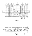
- a second embodiment, illustrated in Figures 5 and 6 is similar to that described in Figures 2 and 3 , except that only the patterns 30, separated from the membranes by the shortest distance D2, are covered with the reflective layer 14.
- the passivation layer 12 has a non-zero reflection power, but less than that of the layer 14.
- the contribution of the most distant units 32 is reduced. This has the effect, on the one hand, of offering an additional means of modulating the respective reflection powers, and therefore the sensitivity spectrum resulting from the detector, but also, very advantageously, of saving a lithographic level during the manufacture of the detector. structure.
- the reflector extends over the entire reflecting surface, it is necessary to implement a lithographic level to define the texturing, and another lithographic level to delimit the contours of the reflector (if not all structures would be in circuit).
- the lithographic level necessary for the definition of the reflector is used at the same time to define the texturing of the reflective surface. The process is simplified and therefore more economical.
- the ratio of the surfaces between the different patterns makes it possible to modulate the contribution of each type of pattern.
- the surface ratio between the separate patterns of the membranes of the distance D1 and the separate patterns of the membranes 16, 18, 20 of the distance D2 is between about 35% and about 65% depending on the type of response sought.
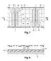
- the second embodiment differs from the first embodiment in that the three-dimensional patterns are arranged as a regular checkerboard.
- the ratio of the surfaces of the two types of patterns is thus substantially equal to 50%. This figure is given for illustrative purposes, and is not preferential.
- This third embodiment is similar to the previous ones with the difference that patterns, shapes and dimensions identical to those of the first embodiment described in relation to the Figures 2 and 3 , are formed in the membranes.
- An advantage of forming the patterns in the membranes and not in the substrate is that the sensitivity of the detector to diffraction phenomena occurring on three-dimensional patterns in the substrate is substantially eliminated.
- a disadvantage is a more complex fabrication. Indeed, the formation of patterns in the substrate is easier.
- the three-dimensional patterns are formed both in the substrate and the membranes, for example to obtain a compromise between ease of construction and attenuation of the diffraction phenomena.
- substantially planar patterns form parallel surface cavities
- other types of patterns may be used.
- the surface of the substrate and / or the membrane has a corrugated profile, for example of the sinusoidal type.
- the present invention finds application in the field of bolometric detection image sensors, whatever the detection frequency band or the type of bolometric material used to manufacture the imaging and reference bolometers, as for example.
- a-Si amorphous silicon
- VOx vanadium oxide
- Ti metal oxide
Landscapes
- Physics & Mathematics (AREA)
- General Physics & Mathematics (AREA)
- Spectroscopy & Molecular Physics (AREA)
- Photometry And Measurement Of Optical Pulse Characteristics (AREA)
- Radiation Pyrometers (AREA)
Applications Claiming Priority (1)
| Application Number | Priority Date | Filing Date | Title |
|---|---|---|---|
| FR0705271A FR2919049B1 (fr) | 2007-07-20 | 2007-07-20 | Detecteur de rayonnement electromagnetique et procede de fabrication d'un tel detecteur |
Publications (2)
| Publication Number | Publication Date |
|---|---|
| EP2019301A1 true EP2019301A1 (de) | 2009-01-28 |
| EP2019301B1 EP2019301B1 (de) | 2013-05-01 |
Family
ID=39283854
Family Applications (1)
| Application Number | Title | Priority Date | Filing Date |
|---|---|---|---|
| EP08305392.6A Not-in-force EP2019301B1 (de) | 2007-07-20 | 2008-07-10 | Elektromagnetische Strahlensonde und Herstellungsverfahren einer solchen Sonde |
Country Status (7)
| Country | Link |
|---|---|
| US (1) | US7999227B2 (de) |
| EP (1) | EP2019301B1 (de) |
| JP (1) | JP5459996B2 (de) |
| CN (1) | CN101349592B (de) |
| CA (1) | CA2637223C (de) |
| FR (1) | FR2919049B1 (de) |
| RU (1) | RU2473872C2 (de) |
Families Citing this family (7)
| Publication number | Priority date | Publication date | Assignee | Title |
|---|---|---|---|---|
| JP5728978B2 (ja) * | 2011-02-02 | 2015-06-03 | セイコーエプソン株式会社 | 熱型光検出器、熱型光検出装置、および電子機器 |
| JP5708020B2 (ja) * | 2011-02-24 | 2015-04-30 | セイコーエプソン株式会社 | 熱型光検出器、熱型光検出装置、電子機器および熱型光検出器の製造方法 |
| US20170030775A1 (en) * | 2014-04-18 | 2017-02-02 | Nec Corporation | Terahertz-wave detector |
| FR3042272B1 (fr) * | 2015-10-09 | 2017-12-15 | Commissariat Energie Atomique | Bolometre a forte sensibilite spectrale. |
| JP6834974B2 (ja) * | 2015-11-04 | 2021-02-24 | 日本電気株式会社 | ボロメータ型テラヘルツ波検出器 |
| FR3059772B1 (fr) * | 2016-12-06 | 2019-05-17 | Safran Electronics & Defense | Systeme de detection de rayonnements electromagnetiques |
| FR3155299B1 (fr) * | 2023-11-13 | 2025-10-24 | Commissariat Energie Atomique | Detecteur thermique large bande et à plusieurs cavités quart d’onde |
Citations (4)
| Publication number | Priority date | Publication date | Assignee | Title |
|---|---|---|---|---|
| US5912464A (en) * | 1996-08-08 | 1999-06-15 | Commissariat Al'energie Atomique | Infrared detector and manufacturing process |
| WO2000037906A1 (en) * | 1998-12-18 | 2000-06-29 | Daewoo Electronics Co., Ltd. | Infrared bolometer and method for the manufacture thereof |
| FR2796148A1 (fr) | 1999-07-08 | 2001-01-12 | Commissariat Energie Atomique | Detecteur bolometrique a isolation electrique intermediaire et procede de fabrication de ce detecteur |
| US6198098B1 (en) * | 1998-05-26 | 2001-03-06 | Philips Laou | Microstructure for infrared detector and method of making same |
Family Cites Families (7)
| Publication number | Priority date | Publication date | Assignee | Title |
|---|---|---|---|---|
| JP2674545B2 (ja) * | 1995-01-20 | 1997-11-12 | 日本電気株式会社 | 赤外線検出器及びその駆動方法 |
| JP2000146684A (ja) * | 1998-11-12 | 2000-05-26 | Nec Corp | 傾斜したダイアフラム構造を有する熱型赤外線検出素子 |
| JP3597069B2 (ja) * | 1999-01-12 | 2004-12-02 | 日本電気株式会社 | 複数の赤外波長帯を検出する熱型赤外アレイセンサ |
| JP3921320B2 (ja) * | 2000-01-31 | 2007-05-30 | 日本電気株式会社 | 熱型赤外線検出器およびその製造方法 |
| JP2002221449A (ja) * | 2001-01-26 | 2002-08-09 | Nikon Corp | 放射検出装置 |
| FR2875298B1 (fr) * | 2004-09-16 | 2007-03-02 | Commissariat Energie Atomique | Detecteur thermique de rayonnement electromagnetique comportant une membrane absorbante fixee en suspension |
| JP4208846B2 (ja) * | 2005-02-10 | 2009-01-14 | 株式会社東芝 | 非冷却赤外線検出素子 |
-
2007
- 2007-07-20 FR FR0705271A patent/FR2919049B1/fr not_active Expired - Fee Related
-
2008
- 2008-07-10 CA CA2637223A patent/CA2637223C/fr not_active Expired - Fee Related
- 2008-07-10 US US12/170,669 patent/US7999227B2/en not_active Expired - Fee Related
- 2008-07-10 EP EP08305392.6A patent/EP2019301B1/de not_active Not-in-force
- 2008-07-17 CN CN200810133552.4A patent/CN101349592B/zh not_active Expired - Fee Related
- 2008-07-17 JP JP2008186406A patent/JP5459996B2/ja not_active Expired - Fee Related
- 2008-07-18 RU RU2008129811/28A patent/RU2473872C2/ru not_active IP Right Cessation
Patent Citations (4)
| Publication number | Priority date | Publication date | Assignee | Title |
|---|---|---|---|---|
| US5912464A (en) * | 1996-08-08 | 1999-06-15 | Commissariat Al'energie Atomique | Infrared detector and manufacturing process |
| US6198098B1 (en) * | 1998-05-26 | 2001-03-06 | Philips Laou | Microstructure for infrared detector and method of making same |
| WO2000037906A1 (en) * | 1998-12-18 | 2000-06-29 | Daewoo Electronics Co., Ltd. | Infrared bolometer and method for the manufacture thereof |
| FR2796148A1 (fr) | 1999-07-08 | 2001-01-12 | Commissariat Energie Atomique | Detecteur bolometrique a isolation electrique intermediaire et procede de fabrication de ce detecteur |
Also Published As
| Publication number | Publication date |
|---|---|
| FR2919049B1 (fr) | 2009-10-02 |
| JP5459996B2 (ja) | 2014-04-02 |
| CA2637223C (fr) | 2016-09-20 |
| CN101349592B (zh) | 2013-07-17 |
| CA2637223A1 (fr) | 2009-01-20 |
| JP2009025306A (ja) | 2009-02-05 |
| RU2008129811A (ru) | 2010-01-27 |
| US20090020702A1 (en) | 2009-01-22 |
| CN101349592A (zh) | 2009-01-21 |
| FR2919049A1 (fr) | 2009-01-23 |
| RU2473872C2 (ru) | 2013-01-27 |
| US7999227B2 (en) | 2011-08-16 |
| EP2019301B1 (de) | 2013-05-01 |
Similar Documents
| Publication | Publication Date | Title |
|---|---|---|
| EP2450681B1 (de) | Infrarotdetektor auf der Basis von hängenden bolometrischen Mikroplatten | |
| EP2019301B1 (de) | Elektromagnetische Strahlensonde und Herstellungsverfahren einer solchen Sonde | |
| EP3239671B1 (de) | Vorrichtung zur erfassung von elektromagnetischer strahlung mit einer einkapselungsstruktur, die mindestens einen interferenzfilter umfasst | |
| EP2602598B1 (de) | Bolometrischer Detektor für elektromagnetische Strahlung im Spektralbereich von Terahertz und Matrix, die solche Detektoren umfasst | |
| EP0828145B1 (de) | Infrarot-Detektor und Verfahren zu dessen Herstellung | |
| EP2613181B1 (de) | Infrarotdetektor mit gehäuse mit mindestens einem integrierten beugungsgitter | |
| EP2324377B1 (de) | Nanostrukturiertes spektralfilter, bildsensor und herstellungsverfahren | |
| EP1715315B1 (de) | Bolometrischer Detektor, Vorricthung zur Detektion elektromagnetischer Submillimeter- und Millimeterwellen mit einem solchen Detektor | |
| EP2084503B1 (de) | Integrierte monolithische interferenzerkennungsvorrichtung | |
| EP3607585B1 (de) | Vorrichtung und verfahren zur multispektralen bildgebung im infrarotbereich | |
| EP0749007A1 (de) | Bolometrische Detektorvorrichtung für Millimeter- und Submillimeterwellen und Herstellungsverfahren für diese Vorrichtung | |
| EP1524507B1 (de) | Bolometer, Infrarotdetektionsvorrichtung diese anwendend und Verfahren zur Herstellung davon | |
| EP1637854B1 (de) | Bolometrische Detektorvorrichtung für infrarote Strahlung | |
| EP1399722B1 (de) | Mikrobolometer und verfahren zu dessen herstellung | |
| EP1482289B1 (de) | Bolometrisches Detetektionsverfahren für (Sub-)Millimeterwellen anhand eines antennengekoppelten Bolometers mit einem Hohlraum | |
| EP2891876A1 (de) | Optischer Detektor eines Gases | |
| EP1880176B1 (de) | Thermischer detektor für elektromagnetische strahlung in einer die detektoren verwendenden infrarot-detektionseinrichtung | |
| EP2746826B1 (de) | Optischer Frequenzfilter und Detektor, der mit einem solchen Filter ausgestattet ist | |
| EP4553465A1 (de) | Breitbandiger thermischer detektor mit mehreren viertelwellen-kavitäten | |
| FR2885690A1 (fr) | Detecteur thermique de rayonnements electromagnetiques et dispositif de detection infrarouge mettant en oeuvre de tels detecteurs | |
| FR3066017A1 (fr) | Dispositif pyroelectrique de detection infrarouge comportant un emetteur infrarouge de modulation | |
| FR2805052A1 (fr) | Filtre fabry-perot court a couches metalliques | |
| FR3159438A1 (fr) | Mire de resolution pour l’imagerie infrarouge | |
| EP3846209A1 (de) | Sensorbauteil mit schwarzen pixeln, und verfahren zur herstellung eines solchen bauteils |
Legal Events
| Date | Code | Title | Description |
|---|---|---|---|
| PUAI | Public reference made under article 153(3) epc to a published international application that has entered the european phase |
Free format text: ORIGINAL CODE: 0009012 |
|
| AK | Designated contracting states |
Kind code of ref document: A1 Designated state(s): AT BE BG CH CY CZ DE DK EE ES FI FR GB GR HR HU IE IS IT LI LT LU LV MC MT NL NO PL PT RO SE SI SK TR |
|
| AX | Request for extension of the european patent |
Extension state: AL BA MK RS |
|
| 17P | Request for examination filed |
Effective date: 20090213 |
|
| 17Q | First examination report despatched |
Effective date: 20090312 |
|
| AKX | Designation fees paid |
Designated state(s): DE FR GB IT SE |
|
| GRAP | Despatch of communication of intention to grant a patent |
Free format text: ORIGINAL CODE: EPIDOSNIGR1 |
|
| GRAS | Grant fee paid |
Free format text: ORIGINAL CODE: EPIDOSNIGR3 |
|
| GRAA | (expected) grant |
Free format text: ORIGINAL CODE: 0009210 |
|
| AK | Designated contracting states |
Kind code of ref document: B1 Designated state(s): DE FR GB IT SE |
|
| REG | Reference to a national code |
Ref country code: GB Ref legal event code: FG4D Free format text: NOT ENGLISH |
|
| REG | Reference to a national code |
Ref country code: DE Ref legal event code: R096 Ref document number: 602008024247 Country of ref document: DE Effective date: 20130627 |
|
| REG | Reference to a national code |
Ref country code: SE Ref legal event code: TRGR |
|
| PLBE | No opposition filed within time limit |
Free format text: ORIGINAL CODE: 0009261 |
|
| STAA | Information on the status of an ep patent application or granted ep patent |
Free format text: STATUS: NO OPPOSITION FILED WITHIN TIME LIMIT |
|
| 26N | No opposition filed |
Effective date: 20140204 |
|
| REG | Reference to a national code |
Ref country code: DE Ref legal event code: R097 Ref document number: 602008024247 Country of ref document: DE Effective date: 20140204 |
|
| PGFP | Annual fee paid to national office [announced via postgrant information from national office to epo] |
Ref country code: IT Payment date: 20150710 Year of fee payment: 8 |
|
| REG | Reference to a national code |
Ref country code: FR Ref legal event code: PLFP Year of fee payment: 9 |
|
| REG | Reference to a national code |
Ref country code: FR Ref legal event code: PLFP Year of fee payment: 10 |
|
| PG25 | Lapsed in a contracting state [announced via postgrant information from national office to epo] |
Ref country code: IT Free format text: LAPSE BECAUSE OF NON-PAYMENT OF DUE FEES Effective date: 20160710 |
|
| REG | Reference to a national code |
Ref country code: FR Ref legal event code: PLFP Year of fee payment: 11 |
|
| PGFP | Annual fee paid to national office [announced via postgrant information from national office to epo] |
Ref country code: DE Payment date: 20190711 Year of fee payment: 12 Ref country code: FR Payment date: 20190723 Year of fee payment: 12 Ref country code: SE Payment date: 20190722 Year of fee payment: 12 |
|
| PGFP | Annual fee paid to national office [announced via postgrant information from national office to epo] |
Ref country code: GB Payment date: 20190719 Year of fee payment: 12 |
|
| REG | Reference to a national code |
Ref country code: DE Ref legal event code: R119 Ref document number: 602008024247 Country of ref document: DE |
|
| REG | Reference to a national code |
Ref country code: SE Ref legal event code: EUG |
|
| GBPC | Gb: european patent ceased through non-payment of renewal fee |
Effective date: 20200710 |
|
| PG25 | Lapsed in a contracting state [announced via postgrant information from national office to epo] |
Ref country code: GB Free format text: LAPSE BECAUSE OF NON-PAYMENT OF DUE FEES Effective date: 20200710 Ref country code: FR Free format text: LAPSE BECAUSE OF NON-PAYMENT OF DUE FEES Effective date: 20200731 |
|
| PG25 | Lapsed in a contracting state [announced via postgrant information from national office to epo] |
Ref country code: DE Free format text: LAPSE BECAUSE OF NON-PAYMENT OF DUE FEES Effective date: 20210202 Ref country code: SE Free format text: LAPSE BECAUSE OF NON-PAYMENT OF DUE FEES Effective date: 20200711 |