EP2019421A2 - Dispositif semi-conducteur de puissance avec couche de contact métallique et procédé de fabrication correspondant - Google Patents
Dispositif semi-conducteur de puissance avec couche de contact métallique et procédé de fabrication correspondant Download PDFInfo
- Publication number
- EP2019421A2 EP2019421A2 EP08008715A EP08008715A EP2019421A2 EP 2019421 A2 EP2019421 A2 EP 2019421A2 EP 08008715 A EP08008715 A EP 08008715A EP 08008715 A EP08008715 A EP 08008715A EP 2019421 A2 EP2019421 A2 EP 2019421A2
- Authority
- EP
- European Patent Office
- Prior art keywords
- power semiconductor
- layer
- pressure
- semiconductor component
- semiconductor device
- Prior art date
- Legal status (The legal status is an assumption and is not a legal conclusion. Google has not performed a legal analysis and makes no representation as to the accuracy of the status listed.)
- Withdrawn
Links
Images

Classifications
-
- H—ELECTRICITY
- H10—SEMICONDUCTOR DEVICES; ELECTRIC SOLID-STATE DEVICES NOT OTHERWISE PROVIDED FOR
- H10W—GENERIC PACKAGES, INTERCONNECTIONS, CONNECTORS OR OTHER CONSTRUCTIONAL DETAILS OF DEVICES COVERED BY CLASS H10
- H10W72/00—Interconnections or connectors in packages
- H10W72/01—Manufacture or treatment
- H10W72/019—Manufacture or treatment of bond pads
-
- H—ELECTRICITY
- H10—SEMICONDUCTOR DEVICES; ELECTRIC SOLID-STATE DEVICES NOT OTHERWISE PROVIDED FOR
- H10W—GENERIC PACKAGES, INTERCONNECTIONS, CONNECTORS OR OTHER CONSTRUCTIONAL DETAILS OF DEVICES COVERED BY CLASS H10
- H10W72/00—Interconnections or connectors in packages
- H10W72/90—Bond pads, in general
-
- H—ELECTRICITY
- H10—SEMICONDUCTOR DEVICES; ELECTRIC SOLID-STATE DEVICES NOT OTHERWISE PROVIDED FOR
- H10D—INORGANIC ELECTRIC SEMICONDUCTOR DEVICES
- H10D30/00—Field-effect transistors [FET]
- H10D30/80—FETs having rectifying junction gate electrodes
- H10D30/83—FETs having PN junction gate electrodes
- H10D30/831—Vertical FETs having PN junction gate electrodes
-
- H—ELECTRICITY
- H10—SEMICONDUCTOR DEVICES; ELECTRIC SOLID-STATE DEVICES NOT OTHERWISE PROVIDED FOR
- H10W—GENERIC PACKAGES, INTERCONNECTIONS, CONNECTORS OR OTHER CONSTRUCTIONAL DETAILS OF DEVICES COVERED BY CLASS H10
- H10W72/00—Interconnections or connectors in packages
- H10W72/01—Manufacture or treatment
- H10W72/019—Manufacture or treatment of bond pads
- H10W72/01921—Manufacture or treatment of bond pads using local deposition
- H10W72/01923—Manufacture or treatment of bond pads using local deposition in liquid form, e.g. by dispensing droplets or by screen printing
-
- H—ELECTRICITY
- H10—SEMICONDUCTOR DEVICES; ELECTRIC SOLID-STATE DEVICES NOT OTHERWISE PROVIDED FOR
- H10W—GENERIC PACKAGES, INTERCONNECTIONS, CONNECTORS OR OTHER CONSTRUCTIONAL DETAILS OF DEVICES COVERED BY CLASS H10
- H10W72/00—Interconnections or connectors in packages
- H10W72/01—Manufacture or treatment
- H10W72/019—Manufacture or treatment of bond pads
- H10W72/01961—Chemical or physical modification, e.g. by sintering or anodisation
-
- H—ELECTRICITY
- H10—SEMICONDUCTOR DEVICES; ELECTRIC SOLID-STATE DEVICES NOT OTHERWISE PROVIDED FOR
- H10W—GENERIC PACKAGES, INTERCONNECTIONS, CONNECTORS OR OTHER CONSTRUCTIONAL DETAILS OF DEVICES COVERED BY CLASS H10
- H10W72/00—Interconnections or connectors in packages
- H10W72/01—Manufacture or treatment
- H10W72/0198—Manufacture or treatment batch processes
-
- H—ELECTRICITY
- H10—SEMICONDUCTOR DEVICES; ELECTRIC SOLID-STATE DEVICES NOT OTHERWISE PROVIDED FOR
- H10W—GENERIC PACKAGES, INTERCONNECTIONS, CONNECTORS OR OTHER CONSTRUCTIONAL DETAILS OF DEVICES COVERED BY CLASS H10
- H10W72/00—Interconnections or connectors in packages
- H10W72/071—Connecting or disconnecting
- H10W72/0711—Apparatus therefor
- H10W72/07141—Means for applying energy, e.g. ovens or lasers
-
- H—ELECTRICITY
- H10—SEMICONDUCTOR DEVICES; ELECTRIC SOLID-STATE DEVICES NOT OTHERWISE PROVIDED FOR
- H10W—GENERIC PACKAGES, INTERCONNECTIONS, CONNECTORS OR OTHER CONSTRUCTIONAL DETAILS OF DEVICES COVERED BY CLASS H10
- H10W72/00—Interconnections or connectors in packages
- H10W72/90—Bond pads, in general
- H10W72/921—Structures or relative sizes of bond pads
- H10W72/923—Bond pads having multiple stacked layers
-
- H—ELECTRICITY
- H10—SEMICONDUCTOR DEVICES; ELECTRIC SOLID-STATE DEVICES NOT OTHERWISE PROVIDED FOR
- H10W—GENERIC PACKAGES, INTERCONNECTIONS, CONNECTORS OR OTHER CONSTRUCTIONAL DETAILS OF DEVICES COVERED BY CLASS H10
- H10W72/00—Interconnections or connectors in packages
- H10W72/90—Bond pads, in general
- H10W72/921—Structures or relative sizes of bond pads
- H10W72/926—Multiple bond pads having different sizes
-
- H—ELECTRICITY
- H10—SEMICONDUCTOR DEVICES; ELECTRIC SOLID-STATE DEVICES NOT OTHERWISE PROVIDED FOR
- H10W—GENERIC PACKAGES, INTERCONNECTIONS, CONNECTORS OR OTHER CONSTRUCTIONAL DETAILS OF DEVICES COVERED BY CLASS H10
- H10W72/00—Interconnections or connectors in packages
- H10W72/90—Bond pads, in general
- H10W72/941—Dispositions of bond pads
- H10W72/942—Dispositions of bond pads relative to underlying supporting features, e.g. bond pads, RDLs or vias
-
- H—ELECTRICITY
- H10—SEMICONDUCTOR DEVICES; ELECTRIC SOLID-STATE DEVICES NOT OTHERWISE PROVIDED FOR
- H10W—GENERIC PACKAGES, INTERCONNECTIONS, CONNECTORS OR OTHER CONSTRUCTIONAL DETAILS OF DEVICES COVERED BY CLASS H10
- H10W72/00—Interconnections or connectors in packages
- H10W72/90—Bond pads, in general
- H10W72/941—Dispositions of bond pads
- H10W72/944—Dispositions of multiple bond pads
-
- H—ELECTRICITY
- H10—SEMICONDUCTOR DEVICES; ELECTRIC SOLID-STATE DEVICES NOT OTHERWISE PROVIDED FOR
- H10W—GENERIC PACKAGES, INTERCONNECTIONS, CONNECTORS OR OTHER CONSTRUCTIONAL DETAILS OF DEVICES COVERED BY CLASS H10
- H10W72/00—Interconnections or connectors in packages
- H10W72/90—Bond pads, in general
- H10W72/951—Materials of bond pads
- H10W72/952—Materials of bond pads comprising metals or metalloids, e.g. PbSn, Ag or Cu
Definitions
- the invention describes a power semiconductor component of at least one contact metallization, preferably with a monocrystalline base body and at least one pn junction.
- Such power semiconductor components are exemplary power diodes, power transistors or power thyristors, but also solar cells and resistance components.
- the contact metallization serves for the electrically conductive connection of contact surfaces of the semiconductor body with external connection elements.
- Such connecting elements may be formed by way of example as wire bonds, substrates connected by soldering or pressure-contacted connecting elements.
- connection element For use in pressure-contacted arrangements, it is also known to arrange a metal disc with a thickness of the order of millimeters between the connection element and the power semiconductor component. This metal disc serves to reduce mechanical stresses on the power semiconductor component or its contact metallization.
- the invention has the object of developing a power semiconductor component in the area of the contact metallization, so that the contact properties are improved and to provide a method whereby the power semiconductor component of a simple production is accessible.
- the starting point of the invention is a power semiconductor component, preferably with a monocrystalline base body and at least one pn junction.
- this power semiconductor component has at least one contact surface, wherein at least one first thin metallic layer of a first material is arranged on this contact surface.
- On at least one of these first metallic layers one, in comparison to this, thicker metallic layer of a second material is arranged.
- the second metallic material has a proportion of more than 90 of 100 of a noble metal. It is particularly preferred here if this noble metal is silver.
- the pasty layer is applied by means of a stencil printing process.
- the necessary positioning accuracy, at the required layer thickness can be achieved.
- this method is inexpensive to implement.
- a first advantageous embodiment of the pressurization of the pasty layer can be given by the application of a press and two press punches.
- at least one press ram is formed with a silicone cushion which generates quasi-hydrostatic pressure thereon.
- a second advantageous embodiment of the pressurization of the pasty layer can be carried out by the application of a filled with a suitable liquid or gas pressure tank.
- a suitable liquid or gas pressure tank it is preferable to arrange the power semiconductor components in the wafer composite and by means of a foil, preferably a teflon foil, covered in the pressure tank and then to apply pressure to the liquid in the latter from outside.
- Fig. 1 and 2 show individual steps of the inventive manufacturing method of a first power semiconductor device according to the invention.
- Fig. 3 shows a second inventive power semiconductor device.
- Fig. 1 and 2 show individual steps of the inventive manufacturing method of a first power semiconductor device according to the invention.
- Fig. 1 is the semiconductor body with the later edges (12) of the power semiconductor devices (10) and in this semiconductor body in a schematic manner a plurality of contact surfaces (20, 22, 24) on the two major surfaces (102, 104).
- the production of the first thin layer of the first metallic material (36) is shown.
- vapor deposition methods by means of shadow masks (38) or sputtering methods are used by way of example.
- At least one homogenous layer with a layer thickness on the order of micrometers is deposited by means of these processes known for many years. In this case, it may well be preferable to deposit this layer from a plurality of thin individual layers of different metals, each with a different layer thickness.
- a pasty layer (44, FIG. Fig. 2 ), as known from sintered joints according to the prior art, arranged on the first layer (34).
- the layers (34, 44) are arranged directly above one another, or whether the pasty second layer (44) slightly covers or does not completely cover the first layer (34).
- the pasty layer (44, Fig. 2 ) itself consists of a mixture of a metallic material in the form of metal flakes with a maximum extent of the order of microns and a solvent.
- the material of the metal flakes is especially silver, but also other precious metals or mixtures with a precious metal content of more than 90 out of 100.
- Fig. 2 shows the pressurization (60) on the pasty layer (44) to form a, compared to the first, thicker second metallic layer.
- a film (50) for example a Teflon film, which was applied before the pressurization (60).
- the maximum applied discharge pressure (60) corresponds to at least 15MPa.
- This second metallic layer has a preferred thickness between 10 .mu.m and 80 .mu.m after the pressurization (60), wherein layers between 1 .mu.m and 250 .mu.m can also be produced and, depending on the application, also make sense.
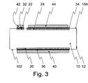
- Fig. 3 shows a second inventive power semiconductor device (10), here a power thyristor. Its semiconductor body has on its first main surface (102) a first contact surface (20), here the cathode, and on its second main surface (104) two further contact surfaces (22, 24), a control input, the gate (22), and an anode (24). In this embodiment, all these contact surfaces are developed according to the invention.
- Each contact surface (20, 22, 24) has a first layer of a first metallic material (30, 32, 34), in this case partial layers of different materials with a last partial layer of silver and a total layer thickness of approximately 5 ⁇ m.
- This first material (30, 32, 34) is covered by a second metallic material (40, 42, 44) arranged by means of a pressure sintering method, here likewise silver with a layer thickness of 50 ⁇ m.
- Such a designed power semiconductor device (10) has the advantage of ease of manufacture (see. Fig. 1 and 2 ) on.
- a power semiconductor component (10) can be used in a pressure-contacted configuration, without a further metallic disk having a thickness in the range from 0.2 mm to 4 mm being arranged between the connection element (not shown) and the power semiconductor component (10) itself. The task of this disc is taken over by the thick second metallic layer (40, 42, 44).
- the advantages of the power semiconductor component (10) according to the invention are also advantageous in combination with other connection techniques. Especially for the production of a sintered connection of the power semiconductor component (10) with a substrate, it is necessary for the power semiconductor component (10) to have a Has precious metal surface for connection. In addition, it is advantageous if this noble metal surface has a layer thickness which is more than 10 ⁇ m. Such layers can be produced much easier and more cost-effectively with the method described in comparison to production by standard methods, for example by means of a sputtering or sputtering method.
Landscapes
- Electrodes Of Semiconductors (AREA)
- Internal Circuitry In Semiconductor Integrated Circuit Devices (AREA)
- Die Bonding (AREA)
Applications Claiming Priority (1)
| Application Number | Priority Date | Filing Date | Title |
|---|---|---|---|
| DE102007022338A DE102007022338B4 (de) | 2007-07-26 | 2007-07-26 | Herstellungsverfahren für ein Leistungshalbleiterbauelement mit Metallkontaktschicht |
Publications (2)
| Publication Number | Publication Date |
|---|---|
| EP2019421A2 true EP2019421A2 (fr) | 2009-01-28 |
| EP2019421A3 EP2019421A3 (fr) | 2012-10-31 |
Family
ID=40030257
Family Applications (1)
| Application Number | Title | Priority Date | Filing Date |
|---|---|---|---|
| EP08008715A Withdrawn EP2019421A3 (fr) | 2007-07-26 | 2008-05-09 | Dispositif semi-conducteur de puissance avec couche de contact métallique et procédé de fabrication correspondant |
Country Status (5)
| Country | Link |
|---|---|
| US (1) | US8110925B2 (fr) |
| EP (1) | EP2019421A3 (fr) |
| JP (1) | JP2009033168A (fr) |
| CN (1) | CN101359637B (fr) |
| DE (1) | DE102007022338B4 (fr) |
Families Citing this family (3)
| Publication number | Priority date | Publication date | Assignee | Title |
|---|---|---|---|---|
| WO2012107482A2 (fr) | 2011-02-08 | 2012-08-16 | Abb Research Ltd | Module semi-conducteur de puissance |
| US8586480B1 (en) * | 2012-07-31 | 2013-11-19 | Ixys Corporation | Power MOSFET having selectively silvered pads for clip and bond wire attach |
| DE102019113762B4 (de) * | 2019-05-23 | 2022-04-14 | Semikron Elektronik Gmbh & Co. Kg | Verfahren zur Herstellung eines Leistungshalbleitermoduls |
Family Cites Families (19)
| Publication number | Priority date | Publication date | Assignee | Title |
|---|---|---|---|---|
| DE3414065A1 (de) * | 1984-04-13 | 1985-12-12 | Siemens AG, 1000 Berlin und 8000 München | Anordnung bestehend aus mindestens einem auf einem substrat befestigten elektronischen bauelement und verfahren zur herstellung einer derartigen anordnung |
| EP0330896A3 (fr) * | 1988-03-03 | 1991-01-09 | Siemens Aktiengesellschaft | Procédé pour fixer des composants semi-conducteurs sur des substrats et dispositifs pour sa réalisation |
| EP0460286A3 (en) | 1990-06-06 | 1992-02-26 | Siemens Aktiengesellschaft | Method and arrangement for bonding a semiconductor component to a substrate or for finishing a semiconductor/substrate connection by contactless pressing |
| EP0477600A1 (fr) * | 1990-09-26 | 1992-04-01 | Siemens Aktiengesellschaft | Procédé pour attacher à un substrat un corps semi-conducteur comportant au moins un composant semi-conducteur |
| DE59209470D1 (de) * | 1991-06-24 | 1998-10-01 | Siemens Ag | Halbleiterbauelement und Verfahren zu seiner Herstellung |
| DE4233073A1 (de) | 1992-10-01 | 1994-04-07 | Siemens Ag | Verfahren zum Herstellen eines Halbleiter-Modulaufbaus |
| JP4077888B2 (ja) | 1995-07-21 | 2008-04-23 | 株式会社東芝 | セラミックス回路基板 |
| DE10062108B4 (de) | 2000-12-13 | 2010-04-15 | Infineon Technologies Ag | Leistungsmodul mit verbessertem transienten Wärmewiderstand |
| EP1280196A1 (fr) * | 2001-07-18 | 2003-01-29 | Abb Research Ltd. | Procédé de fixatoin de dispositifs électroniques sur des substrats |
| JP2003101184A (ja) | 2001-09-27 | 2003-04-04 | Kyocera Corp | セラミック回路基板およびその製造方法 |
| TWI239080B (en) * | 2002-12-31 | 2005-09-01 | Advanced Semiconductor Eng | Semiconductor chip package and method for the same |
| DE10349477A1 (de) * | 2003-10-21 | 2005-02-24 | Infineon Technologies Ag | Halbleiterbauteile mit einem Gehäuse und mit einem Halbleiterchip, sowie Verfahren zur Herstellung desselben |
| KR20070033329A (ko) * | 2004-02-18 | 2007-03-26 | 버지니아 테크 인터렉추얼 프라퍼티스, 인크. | 인터커넥트를 위한 나노 크기의 금속 페이스트 및 이의사용 방법 |
| US20070183920A1 (en) * | 2005-02-14 | 2007-08-09 | Guo-Quan Lu | Nanoscale metal paste for interconnect and method of use |
| DE102004019567B3 (de) * | 2004-04-22 | 2006-01-12 | Semikron Elektronik Gmbh & Co. Kg | Verfahren zur Befestigung von elektronischen Bauelementen auf einem Substrat |
| US20070065984A1 (en) * | 2005-09-22 | 2007-03-22 | Lau Daniel K | Thermal enhanced package for block mold assembly |
| DE102005047566C5 (de) * | 2005-10-05 | 2011-06-09 | Semikron Elektronik Gmbh & Co. Kg | Anordnung mit einem Leistungshalbleiterbauelement und mit einem Gehäuse sowie Herstellungsverfahren hierzu |
| DE102005058794A1 (de) * | 2005-12-09 | 2007-06-14 | Semikron Elektronik Gmbh & Co. Kg | Vorrichtung und getaktetes Verfahren zur Drucksinterverbindung |
| US8067256B2 (en) * | 2007-09-28 | 2011-11-29 | Intel Corporation | Method of making microelectronic package using integrated heat spreader stiffener panel and microelectronic package formed according to the method |
-
2007
- 2007-07-26 DE DE102007022338A patent/DE102007022338B4/de active Active
-
2008
- 2008-05-09 EP EP08008715A patent/EP2019421A3/fr not_active Withdrawn
- 2008-07-24 CN CN2008101300718A patent/CN101359637B/zh active Active
- 2008-07-24 JP JP2008191058A patent/JP2009033168A/ja active Pending
- 2008-07-28 US US12/220,826 patent/US8110925B2/en not_active Expired - Fee Related
Non-Patent Citations (1)
| Title |
|---|
| CHRISTIAN MERTENS: "Die Niedertemperatur-Vervindungstechnik der Leistungselektronik", 2004, VDI VERLAG, Hannover, ISBN: 3-18-336521-9, pages: 73-80 * |
Also Published As
| Publication number | Publication date |
|---|---|
| CN101359637B (zh) | 2012-08-29 |
| CN101359637A (zh) | 2009-02-04 |
| DE102007022338B4 (de) | 2013-12-05 |
| JP2009033168A (ja) | 2009-02-12 |
| US8110925B2 (en) | 2012-02-07 |
| DE102007022338A1 (de) | 2009-04-09 |
| EP2019421A3 (fr) | 2012-10-31 |
| US20090039516A1 (en) | 2009-02-12 |
Similar Documents
| Publication | Publication Date | Title |
|---|---|---|
| DE102010021764B4 (de) | Verfahren zur Niedertemperatur Drucksinterverbindung zweier Verbindungspartner | |
| DE102004019567B3 (de) | Verfahren zur Befestigung von elektronischen Bauelementen auf einem Substrat | |
| DE102004056702B3 (de) | Verfahren zur Befestigung von elektronischen Bauelementen auf einem Substrat | |
| EP1993133B1 (fr) | Procédé de fabrication d'un substrat semi-conducteur de puissance fritté | |
| DE102010021765B4 (de) | Herstellungsverfahren zur Anordnung zweier Verbindungspartner mittels einer Niedertemperatur Drucksinterverbindung | |
| DE112017000426B4 (de) | Leistungshalbleitervorrichtung und verfahren zum herstellen einer leistungshalbleitervorrichtung | |
| DE102007054710B3 (de) | Verfahren zur Herstellung einer Halbleiterbaugruppe | |
| EP1989741A2 (fr) | Procede pour produire des modules a effet peltier, et module peltier ainsi obtenu | |
| DE102012213548A1 (de) | Bondpad zum Thermokompressionsbonden, Verfahren zum Herstellen eines Bondpads und Bauelement | |
| EP2345095B1 (fr) | Actionneur piézoélectrique de construction multicouche et procédé de fixation d'une électrode extérieure sur un actionneur piézoélectrique | |
| DE19522338B4 (de) | Chipträgeranordnung mit einer Durchkontaktierung | |
| EP2498283B1 (fr) | Procédé de fabrication de substrat semi-conducteur de puissance | |
| DE112018003432T5 (de) | Halbleitervorrichtung und verfahren zur herstellung vonhalbleiterbauelementen | |
| DE102014109766B3 (de) | Verfahren zum Herstellen eines Substratadapters, Substratadapter und Verfahren zum Kontaktieren eines Halbleiterelements | |
| DE102007022338B4 (de) | Herstellungsverfahren für ein Leistungshalbleiterbauelement mit Metallkontaktschicht | |
| DE69316159T2 (de) | Verfahren zum Aufbringen von Kontakthöckern auf einer Halbleitervorrichtung sowie zum Verbinden dieser Vorrichtung mit einer Leiterplatte | |
| DE102005058654B4 (de) | Verfahren zum flächigen Fügen von Komponenten von Halbleiterbauelementen | |
| EP1993132B1 (fr) | Substrat semi-conducteur de puissance doté d'une couche de contact métallique et procédé de fabrication associé | |
| DE102008055138A1 (de) | Hochtemperaturbeständige lötmittelfreie Bauelementstruktur und Verfahren zum elektrischen Kontaktieren | |
| DE102013102637A1 (de) | Metall-Keramik-Substrat sowie Verfahren zum Herstellen eines Metall-Keramik-Substrates | |
| DE102014116030A1 (de) | Verfahren zur Herstellung einer Verbindung und Anordnung für eine Chipzusammenstellung mit Direktverbindung | |
| DE102009016112A1 (de) | Einrichtung mit einem elektrischen Bauelement und wenigstens einer elektrischen Anschlussleitung | |
| DE102017102035A1 (de) | Halbleitervorrichtung, Verfahren zum Fertigen einer Halbleitervorrichtung und Verfahren zum Verstärken eines Die in einer Halbleitervorrichtung | |
| DE102016124215B4 (de) | Verfahren zur Niedertemperatur-Drucksinterverbindung zweier Verbindungspartner | |
| EP3262679A1 (fr) | Module d'électronique de puissance comprenant un support présentant une couche barrière de diffusion d'oxygène en palladium et un élément semi-conducteur relié audit module par frittage et procédé pour la fabrication dudit module |
Legal Events
| Date | Code | Title | Description |
|---|---|---|---|
| PUAI | Public reference made under article 153(3) epc to a published international application that has entered the european phase |
Free format text: ORIGINAL CODE: 0009012 |
|
| AK | Designated contracting states |
Kind code of ref document: A2 Designated state(s): AT BE BG CH CY CZ DE DK EE ES FI FR GB GR HR HU IE IS IT LI LT LU LV MC MT NL NO PL PT RO SE SI SK TR |
|
| AX | Request for extension of the european patent |
Extension state: AL BA MK RS |
|
| PUAL | Search report despatched |
Free format text: ORIGINAL CODE: 0009013 |
|
| AK | Designated contracting states |
Kind code of ref document: A3 Designated state(s): AT BE BG CH CY CZ DE DK EE ES FI FR GB GR HR HU IE IS IT LI LT LU LV MC MT NL NO PL PT RO SE SI SK TR |
|
| AX | Request for extension of the european patent |
Extension state: AL BA MK RS |
|
| RIC1 | Information provided on ipc code assigned before grant |
Ipc: H01L 23/485 20060101ALI20120925BHEP Ipc: H01L 23/48 20060101ALI20120925BHEP Ipc: H01L 21/60 20060101AFI20120925BHEP |
|
| 17P | Request for examination filed |
Effective date: 20130502 |
|
| AKX | Designation fees paid |
Designated state(s): AT BE BG CH CY CZ DE DK EE ES FI FR GB GR HR HU IE IS IT LI LT LU LV MC MT NL NO PL PT RO SE SI SK TR |
|
| 17Q | First examination report despatched |
Effective date: 20140417 |
|
| STAA | Information on the status of an ep patent application or granted ep patent |
Free format text: STATUS: THE APPLICATION HAS BEEN WITHDRAWN |
|
| 18W | Application withdrawn |
Effective date: 20161005 |