EP2019453A1 - Schaltungsplattenstecker, Steckverbinder und elektronische Vorrichtung mit einem solchen Schaltungsplattenstecker - Google Patents
Schaltungsplattenstecker, Steckverbinder und elektronische Vorrichtung mit einem solchen Schaltungsplattenstecker Download PDFInfo
- Publication number
- EP2019453A1 EP2019453A1 EP08012633A EP08012633A EP2019453A1 EP 2019453 A1 EP2019453 A1 EP 2019453A1 EP 08012633 A EP08012633 A EP 08012633A EP 08012633 A EP08012633 A EP 08012633A EP 2019453 A1 EP2019453 A1 EP 2019453A1
- Authority
- EP
- European Patent Office
- Prior art keywords
- insulator
- connector
- mating
- shell
- portions
- Prior art date
- Legal status (The legal status is an assumption and is not a legal conclusion. Google has not performed a legal analysis and makes no representation as to the accuracy of the status listed.)
- Granted
Links
Images


Classifications
-
- H—ELECTRICITY
- H01—ELECTRIC ELEMENTS
- H01R—ELECTRICALLY-CONDUCTIVE CONNECTIONS; STRUCTURAL ASSOCIATIONS OF A PLURALITY OF MUTUALLY-INSULATED ELECTRICAL CONNECTING ELEMENTS; COUPLING DEVICES; CURRENT COLLECTORS
- H01R12/00—Structural associations of a plurality of mutually-insulated electrical connecting elements, specially adapted for printed circuits, e.g. printed circuit boards [PCB], flat or ribbon cables, or like generally planar structures, e.g. terminal strips, terminal blocks; Coupling devices specially adapted for printed circuits, flat or ribbon cables, or like generally planar structures; Terminals specially adapted for contact with, or insertion into, printed circuits, flat or ribbon cables, or like generally planar structures
-
- H—ELECTRICITY
- H01—ELECTRIC ELEMENTS
- H01R—ELECTRICALLY-CONDUCTIVE CONNECTIONS; STRUCTURAL ASSOCIATIONS OF A PLURALITY OF MUTUALLY-INSULATED ELECTRICAL CONNECTING ELEMENTS; COUPLING DEVICES; CURRENT COLLECTORS
- H01R12/00—Structural associations of a plurality of mutually-insulated electrical connecting elements, specially adapted for printed circuits, e.g. printed circuit boards [PCB], flat or ribbon cables, or like generally planar structures, e.g. terminal strips, terminal blocks; Coupling devices specially adapted for printed circuits, flat or ribbon cables, or like generally planar structures; Terminals specially adapted for contact with, or insertion into, printed circuits, flat or ribbon cables, or like generally planar structures
- H01R12/70—Coupling devices
- H01R12/71—Coupling devices for rigid printing circuits or like structures
- H01R12/72—Coupling devices for rigid printing circuits or like structures coupling with the edge of the rigid printed circuits or like structures
- H01R12/73—Coupling devices for rigid printing circuits or like structures coupling with the edge of the rigid printed circuits or like structures connecting to other rigid printed circuits or like structures
-
- H—ELECTRICITY
- H01—ELECTRIC ELEMENTS
- H01R—ELECTRICALLY-CONDUCTIVE CONNECTIONS; STRUCTURAL ASSOCIATIONS OF A PLURALITY OF MUTUALLY-INSULATED ELECTRICAL CONNECTING ELEMENTS; COUPLING DEVICES; CURRENT COLLECTORS
- H01R12/00—Structural associations of a plurality of mutually-insulated electrical connecting elements, specially adapted for printed circuits, e.g. printed circuit boards [PCB], flat or ribbon cables, or like generally planar structures, e.g. terminal strips, terminal blocks; Coupling devices specially adapted for printed circuits, flat or ribbon cables, or like generally planar structures; Terminals specially adapted for contact with, or insertion into, printed circuits, flat or ribbon cables, or like generally planar structures
- H01R12/50—Fixed connections
- H01R12/51—Fixed connections for rigid printed circuits or like structures
- H01R12/52—Fixed connections for rigid printed circuits or like structures connecting to other rigid printed circuits or like structures
-
- H—ELECTRICITY
- H01—ELECTRIC ELEMENTS
- H01R—ELECTRICALLY-CONDUCTIVE CONNECTIONS; STRUCTURAL ASSOCIATIONS OF A PLURALITY OF MUTUALLY-INSULATED ELECTRICAL CONNECTING ELEMENTS; COUPLING DEVICES; CURRENT COLLECTORS
- H01R12/00—Structural associations of a plurality of mutually-insulated electrical connecting elements, specially adapted for printed circuits, e.g. printed circuit boards [PCB], flat or ribbon cables, or like generally planar structures, e.g. terminal strips, terminal blocks; Coupling devices specially adapted for printed circuits, flat or ribbon cables, or like generally planar structures; Terminals specially adapted for contact with, or insertion into, printed circuits, flat or ribbon cables, or like generally planar structures
- H01R12/70—Coupling devices
- H01R12/71—Coupling devices for rigid printing circuits or like structures
- H01R12/712—Coupling devices for rigid printing circuits or like structures co-operating with the surface of the printed circuit or with a coupling device exclusively provided on the surface of the printed circuit
- H01R12/716—Coupling device provided on the PCB
-
- H—ELECTRICITY
- H01—ELECTRIC ELEMENTS
- H01R—ELECTRICALLY-CONDUCTIVE CONNECTIONS; STRUCTURAL ASSOCIATIONS OF A PLURALITY OF MUTUALLY-INSULATED ELECTRICAL CONNECTING ELEMENTS; COUPLING DEVICES; CURRENT COLLECTORS
- H01R13/00—Details of coupling devices of the kinds covered by groups H01R12/70 or H01R24/00 - H01R33/00
- H01R13/648—Protective earth or shield arrangements on coupling devices, e.g. anti-static shielding
- H01R13/658—High frequency shielding arrangements, e.g. against EMI [Electro-Magnetic Interference] or EMP [Electro-Magnetic Pulse]
-
- H—ELECTRICITY
- H01—ELECTRIC ELEMENTS
- H01R—ELECTRICALLY-CONDUCTIVE CONNECTIONS; STRUCTURAL ASSOCIATIONS OF A PLURALITY OF MUTUALLY-INSULATED ELECTRICAL CONNECTING ELEMENTS; COUPLING DEVICES; CURRENT COLLECTORS
- H01R13/00—Details of coupling devices of the kinds covered by groups H01R12/70 or H01R24/00 - H01R33/00
- H01R13/648—Protective earth or shield arrangements on coupling devices, e.g. anti-static shielding
- H01R13/658—High frequency shielding arrangements, e.g. against EMI [Electro-Magnetic Interference] or EMP [Electro-Magnetic Pulse]
- H01R13/6591—Specific features or arrangements of connection of shield to conductive members
- H01R13/65912—Specific features or arrangements of connection of shield to conductive members for shielded multiconductor cable
Definitions
- This invention relates to a board connector having an SMT (Surface Mount Technology) terminal, a mating connector to be connected with the board connector, and an electronic device including the board connector and the mating connector.
- SMT Surface Mount Technology
- JP-U 3118719 and JP-A 2005-302417 disclose the conventional type of the connector assembly and discuss the measures against the noise. However, JP-U 3118719 and JP-A 2005-302417 do not present the sufficient countermeasures.
- a board connector comprising a plurality of contacts each having an SMT (Surface Mount Technology) terminal to be connected to a wiring pattern on a board, an insulator ; and a shell covering, at least in part, the insulator.
- the insulator has a first insulator portion extending in a first direction and two second insulator portions each extending in a second direction perpendicular to the first direction.
- the first insulator portion has first ends in the first direction.
- the first insulator portion has a bottom surface.
- Each of the second insulator portions has a second end.
- the second insulator portions extend from the first ends to the second ends, respectively. The second ends are positioned on an imaginary straight line.
- the first insulator portion, the second insulator portions and the imaginary straight line define a predetermined area.
- the first insulator portion holds the plurality of contacts so that the SMT terminal is positioned in the predetermined area or on the bottom surface of the first insulator portion as seen from below the board connector.
- a mating connector fittable with the board connector.
- the mating connector comprises a mating shell.
- the shell of the board connector and the mating shell are positioned over the SMT terminals to electrically shield the SMT terminals.
- the board connector and the mating connector occupying a specific area when the board connector and the mating connector are fitted with each other. Assuming the specific area is equally divided into three regions in the second direction, the SMT terminals are positioned in a middle one of the three regions.
- an electronic apparatus comprising the board connector and the mating connector, wherein the board connector is fitted with the mating connector.
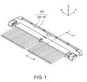
- Fig. 1 is a perspective view of a connector assembly according to an embodiment of the present invention
- Fig. 2 is a perspective view showing a mating connector constituting the connector assembly of Fig. 1 ;
- Fig. 3 is a perspective view of a board connector constituting the connector assembly of Fig. 1 ;
- Fig. 4 is a cross sectional view showing the connector assembly taken along lines IV-IV in Fig. 1 ;
- Fig. 5 is a perspective view of an insulator included in the board connector of Fig. 3 ;
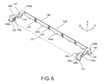
- Fig. 6 is a perspective view of a shell included in the board connector of Fig. 3 ;
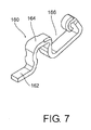
- Fig. 7 shows a contact included in the board connector of Fig. 3 .
- a connector assembly 300 comprises a board connector 100 to be mounted on a board and a mating connector 200 connected to a plurality of cables 400.
- the board connector 100 is fittable with the mating connector 200.
- the connector assembly 300 is generally used in electronic devices such as a cellular phone.
- the mating connector 200 has a mating insulator 220, a mating shell 240, and a plurality of mating contacts 260.
- the mating insulator 220 extends in an X-direction and holds the plurality of mating contacts 260.
- the mating shell 240 extends in the X-direction and covers the mating insulator 220.
- the mating shell 240 is connected to the shield portions 420.
- the mating shell 240 has two end portions 242, a front end portion 244, and two connection portions 246. Each of the end portions 242 protrudes from the mating shell 240 in the X-direction.
- the front end portion 244 is formed on a front end of the mating shell 240 in a Y-direction.
- Each mating contact 260 has a first connect portion 262 to be connected to a signal conductor 440 of the cable 400 and a second connect portion 264 for establishing a connection with the board connector 100.
- the board connector 100 comprises an insulator 120, a shell 140 covering a part of the insulator 120, and a plurality of contacts 160 held by the insulator 120.
- each contact 160 has an SMT (Surface Mount Technology) terminal 162, a contact portion 166, and a coupling portion 164.
- the SMT terminals 162 are connected to a wiring pattern on the board.
- Each contact portion 166 is connected with the first connect portion 264 of the mating contact 260.
- the SMT terminal 162 and the connection portion 166 are coupled by the coupling portion 164.
- the insulator 120 has a first insulator portion 122 extending in the X-direction and two second insulator portions 126 each extending in the Y-direction.
- the first insulator portion 122 has a bottom surface 123 and first ends 122a and 122b in the X-direction.
- Each second insulator portion 126 has a second end 126a, 126b.
- the second insulator portions 126 extend from the first ends 122a and 122b to the second ends 126a and 126b, respectively.
- the second ends 126a and 126b are positioned on an imaginary straight line L1.
- the first insulator portion 122, the second insulator portions 126, and the imaginary straight line L1 define a predetermined area 130 as shown in Fig. 5 .
- the first insulator portion 122 has a plurality of hold portions 124 each holding the contact 160.
- the hold portion 124 is provided with a bottom portion 124a which has a certain thickness. With this structure, when seen from below the board connector 100, the bottom portion 124a hides the contacts 160 except for the SMT terminals 162. This structure enables more effective use of the surface of the board in a way by, for example, forming the wiring patterns on the board at the position directly under the bottom surface 123.
- each hold portion 124 holds the contact 160 so that the SMT terminal 162 is positioned within the predetermined area 130.
- the SMT terminals 162 may be positioned under the first insulator portion 122.
- first insulator portion 122 and the second insulator portions 126 are provided with recesses 122c and recesses 126c, respectively.
- each second insulator portion 126 is provided with a depression 128.
- the shell 140 has a first shell portion 142 covering a part of the first insulator portion 122 and second shell portions 144 covering the second insulator portions 126.
- the first shell portion 142 and the second shell portions 144 are formed integrally with each other.
- the first shell portion 142 has first ends 142a and 142b in the X-direction.
- Each second shell portion 144 has a second end 144a, 144b.
- the second shell portions 144 extend from the first ends 142a and 142b to the second ends 144a and 144b, respectively.
- the second ends 144a and 144b are positioned on an imaginary straight line L2.
- the first shell portion 142 has a plurality of projections 142c projecting downward in a Z-direction.
- each of the second shell portions 144 has a second projection 144c projecting downward in the Z-direction.
- the first projections 142c are pressly-fitted into the recess 122c, respectively.
- the second projections 144c are pressly-fitted into the recess 126c, respectively.
- first shell portion 142 has first spring contact portions 143.
- Each second shell portion 144 has a second spring contact portion 146.
- first spring contact portions 143 and the second spring contact portions 146 are connected to the front end portion 244 and the connection portions 246 of the mating shell 240, respectively.
- each of the second shell portions 144 has a cover 145 covering the depression 128 and a hold-down portion 147 for fixing the board connector 100 to the board.
- a pair of the depression 128 and the cover 145 constitutes a receiver portion which receives the end portion 242 of the mating connector 200 in the Z-direction.
- the shell 140 of the board connector 100 and the mating shell 240 are positioned over the SMT terminals 162 to electrically shield the SMT terminals 162 when the board connector 100 and the mating connector 200 are fitted with each other.
- the board connector 100 and the mating connector 200 occupy a specific area when the board connector 100 and the mating connector 200 are fitted with each other.
- the SMT terminals 162 are positioned in a middle region B of the three regions.
- the mating connector 200 is configured to hold a plurality of cables 400 which extend in a predetermined direction in a plane perpendicular to the X-direction.
- the SMT terminal 162 extends in the predetermined direction when the mating connector 200 holding the cables 400 is fitted with the board connector 100.
- Each of the mating contacts 260 has the first connect portion 264 to be connected to the contact 160 and the second connect portion 262 to be connected to the cable 400.
- Each of the SMT terminals 162 are positioned between the first and the second connect portions 262, 264 in the Y-direction when the mating connector 200 holding the cables 400 is fitted with the board connector 100.
Landscapes
- Details Of Connecting Devices For Male And Female Coupling (AREA)
- Coupling Device And Connection With Printed Circuit (AREA)
Applications Claiming Priority (1)
| Application Number | Priority Date | Filing Date | Title |
|---|---|---|---|
| JP2007195087A JP4522440B2 (ja) | 2007-07-26 | 2007-07-26 | 基板搭載用コネクタ及びその相手方コネクタ並びにそれらを備えた電子機器 |
Publications (2)
| Publication Number | Publication Date |
|---|---|
| EP2019453A1 true EP2019453A1 (de) | 2009-01-28 |
| EP2019453B1 EP2019453B1 (de) | 2013-01-09 |
Family
ID=39730883
Family Applications (1)
| Application Number | Title | Priority Date | Filing Date |
|---|---|---|---|
| EP08012633A Not-in-force EP2019453B1 (de) | 2007-07-26 | 2008-07-11 | Schaltungsplattenstecker, Steckverbinder und elektronische Vorrichtung mit einem solchen Schaltungsplattenstecker |
Country Status (7)
| Country | Link |
|---|---|
| US (1) | US7722387B2 (de) |
| EP (1) | EP2019453B1 (de) |
| JP (1) | JP4522440B2 (de) |
| KR (1) | KR101017178B1 (de) |
| CN (1) | CN101355203B (de) |
| DK (1) | DK2019453T3 (de) |
| TW (1) | TWI378604B (de) |
Cited By (1)
| Publication number | Priority date | Publication date | Assignee | Title |
|---|---|---|---|---|
| TWI867168B (zh) * | 2020-03-03 | 2024-12-21 | 日商日本電產理德股份有限公司 | 基板安裝用連接器 |
Families Citing this family (19)
| Publication number | Priority date | Publication date | Assignee | Title |
|---|---|---|---|---|
| JP4364265B2 (ja) * | 2007-07-26 | 2009-11-11 | 日本航空電子工業株式会社 | コネクタ及びそれを備えた電子機器 |
| JP4704477B2 (ja) * | 2009-02-19 | 2011-06-15 | 日本航空電子工業株式会社 | コネクタ組立体 |
| TWI398993B (zh) * | 2009-03-09 | 2013-06-11 | Hon Hai Prec Ind Co Ltd | 電連接器組件 |
| JP4792517B2 (ja) * | 2009-07-07 | 2011-10-12 | 日本航空電子工業株式会社 | コネクタ組立体 |
| JP4922420B2 (ja) * | 2010-02-23 | 2012-04-25 | 日本航空電子工業株式会社 | コネクタ組立体 |
| WO2012061990A1 (zh) * | 2010-11-11 | 2012-05-18 | 深圳盛凌电子股份有限公司 | 一种pcb板连接器及pcb板连接结构 |
| JP5813349B2 (ja) * | 2011-03-29 | 2015-11-17 | 日本航空電子工業株式会社 | コネクタ及び接続対象物 |
| US8430684B1 (en) * | 2011-08-04 | 2013-04-30 | George F. Glatts, III | Ribbon cable connector |
| US8888506B2 (en) * | 2013-01-29 | 2014-11-18 | Japan Aviation Electronics Industry, Limited | Connector |
| JP6249676B2 (ja) * | 2013-08-21 | 2017-12-20 | 宏致電子股▲ふん▼有限公司Aces Electronics Co.,Ltd. | 電気コネクタ |
| US9065228B2 (en) * | 2013-11-21 | 2015-06-23 | Japan Aviation Electronics Industry, Limited | Connector |
| JP6269558B2 (ja) * | 2014-06-05 | 2018-01-31 | 株式会社村田製作所 | コネクタセット及びコネクタ |
| JP6052268B2 (ja) * | 2014-11-28 | 2016-12-27 | 第一精工株式会社 | 電気コネクタ及び電気コネクタ装置 |
| CN107204532A (zh) * | 2016-03-17 | 2017-09-26 | 泰科电子(上海)有限公司 | 连接器 |
| CN108933342A (zh) * | 2017-05-26 | 2018-12-04 | 昆山宏致电子有限公司 | 线对板连接器组合及其板端连接器 |
| JP7144245B2 (ja) * | 2018-08-31 | 2022-09-29 | 日本航空電子工業株式会社 | はんだ付け部品 |
| JP6859998B2 (ja) | 2018-12-28 | 2021-04-14 | I−Pex株式会社 | 電気コネクタおよびコネクタ装置 |
| TWI740511B (zh) * | 2019-07-10 | 2021-09-21 | 貝爾威勒電子股份有限公司 | 全遮蔽式的排線連接器及其排線插頭 |
| US12555960B2 (en) * | 2023-11-15 | 2026-02-17 | Aces Electronics Co., Ltd. | Shell grounding structure of electrical connector |
Citations (5)
| Publication number | Priority date | Publication date | Assignee | Title |
|---|---|---|---|---|
| JPH03118719U (de) | 1990-03-22 | 1991-12-06 | ||
| WO2005043687A1 (en) | 2003-10-21 | 2005-05-12 | 3M Innovative Properties Company | Connector and connector system |
| JP2005302417A (ja) | 2004-04-08 | 2005-10-27 | Honda Tsushin Kogyo Co Ltd | ケーブル用コネクタ |
| US20060172589A1 (en) * | 2005-02-01 | 2006-08-03 | Hon Hai Precision Ind. Co., Ltd. | Connector assembly having low profile |
| US7207842B1 (en) * | 2005-10-21 | 2007-04-24 | Hirose Electric Co., Ltd. | Electrical connector |
Family Cites Families (10)
| Publication number | Priority date | Publication date | Assignee | Title |
|---|---|---|---|---|
| JPH03119722U (de) * | 1990-03-20 | 1991-12-10 | ||
| JP3119722B2 (ja) | 1992-05-25 | 2000-12-25 | 株式会社小松製作所 | 圧力比例制御弁による4位置クローズドセンタの切換弁の油圧回路 |
| JP3118719B2 (ja) | 1994-06-09 | 2000-12-18 | 日本電池株式会社 | 密閉式非水電解液電池 |
| US5470259A (en) * | 1994-12-05 | 1995-11-28 | The Whitaker Corporation | Grounding shroud for surface mounted electrical connector |
| JP2003007378A (ja) | 2001-06-22 | 2003-01-10 | Sumitomo Wiring Syst Ltd | コネクタ |
| JP2005339985A (ja) * | 2004-05-27 | 2005-12-08 | Kel Corp | コネクタ |
| JP4068092B2 (ja) * | 2004-11-24 | 2008-03-26 | Smk株式会社 | 多極同軸ケーブルコネクタ及びコネクタ組立て方法 |
| JP2006244732A (ja) * | 2005-02-28 | 2006-09-14 | Molex Inc | ケーブル用コネクタ |
| JP4889243B2 (ja) * | 2005-06-09 | 2012-03-07 | モレックス インコーポレイテド | コネクタ装置 |
| JP2007317554A (ja) | 2006-05-26 | 2007-12-06 | Three M Innovative Properties Co | コネクタ及びコネクタシステム |
-
2007
- 2007-07-26 JP JP2007195087A patent/JP4522440B2/ja not_active Expired - Fee Related
-
2008
- 2008-07-01 TW TW097124686A patent/TWI378604B/zh not_active IP Right Cessation
- 2008-07-01 US US12/217,009 patent/US7722387B2/en not_active Expired - Fee Related
- 2008-07-11 EP EP08012633A patent/EP2019453B1/de not_active Not-in-force
- 2008-07-11 DK DK08012633.7T patent/DK2019453T3/da active
- 2008-07-15 KR KR1020080068572A patent/KR101017178B1/ko not_active Expired - Fee Related
- 2008-07-28 CN CN2008101343732A patent/CN101355203B/zh not_active Expired - Fee Related
Patent Citations (5)
| Publication number | Priority date | Publication date | Assignee | Title |
|---|---|---|---|---|
| JPH03118719U (de) | 1990-03-22 | 1991-12-06 | ||
| WO2005043687A1 (en) | 2003-10-21 | 2005-05-12 | 3M Innovative Properties Company | Connector and connector system |
| JP2005302417A (ja) | 2004-04-08 | 2005-10-27 | Honda Tsushin Kogyo Co Ltd | ケーブル用コネクタ |
| US20060172589A1 (en) * | 2005-02-01 | 2006-08-03 | Hon Hai Precision Ind. Co., Ltd. | Connector assembly having low profile |
| US7207842B1 (en) * | 2005-10-21 | 2007-04-24 | Hirose Electric Co., Ltd. | Electrical connector |
Cited By (1)
| Publication number | Priority date | Publication date | Assignee | Title |
|---|---|---|---|---|
| TWI867168B (zh) * | 2020-03-03 | 2024-12-21 | 日商日本電產理德股份有限公司 | 基板安裝用連接器 |
Also Published As
| Publication number | Publication date |
|---|---|
| DK2019453T3 (da) | 2013-02-04 |
| JP4522440B2 (ja) | 2010-08-11 |
| JP2009032518A (ja) | 2009-02-12 |
| US7722387B2 (en) | 2010-05-25 |
| KR20090012081A (ko) | 2009-02-02 |
| CN101355203B (zh) | 2012-11-07 |
| EP2019453B1 (de) | 2013-01-09 |
| TWI378604B (en) | 2012-12-01 |
| KR101017178B1 (ko) | 2011-02-25 |
| TW200919846A (en) | 2009-05-01 |
| CN101355203A (zh) | 2009-01-28 |
| US20090029598A1 (en) | 2009-01-29 |
Similar Documents
| Publication | Publication Date | Title |
|---|---|---|
| EP2019453A1 (de) | Schaltungsplattenstecker, Steckverbinder und elektronische Vorrichtung mit einem solchen Schaltungsplattenstecker | |
| US12027802B2 (en) | Connector | |
| US11158968B2 (en) | Connector and connector assembly | |
| KR100942681B1 (ko) | 전기 커넥터 | |
| EP1471607B1 (de) | Elektrischer Verbinder mit verbesserter Funktion von sowohl der magnetischen Abschirmung als auch der Masseverbindung | |
| US7513786B2 (en) | Connector, circuit board and electronic apparatus | |
| EP2019452B1 (de) | Steckverbinder und elektronische Vorrichtung damit | |
| EP1885028A1 (de) | Steckverbinder mit niedrigem Profil | |
| US9979122B1 (en) | Electronic device and connector | |
| EP3832809B1 (de) | Kabelverbinder | |
| CN101375471A (zh) | 连接器 | |
| US20080176435A1 (en) | Electrical Connector for Flat Cable | |
| JP4184251B2 (ja) | カードコネクタ | |
| JP7176659B2 (ja) | 電気コネクタ | |
| JP5787081B2 (ja) | コネクタ装置 | |
| US6843665B2 (en) | Connector in which contact force can be maintained during a long period | |
| JP4070988B2 (ja) | 平型柔軟ケーブル用コネクタ | |
| EP4601127A1 (de) | Schwimmender verbinder und gegenverbinder dafür | |
| US20090004901A1 (en) | Connector having a stopper mechanism defining a movable range of a housing receiving a connection object | |
| US20260121350A1 (en) | Mating assist mechanism | |
| JP3939235B2 (ja) | コネクタ | |
| KR100655833B1 (ko) | 연성 인쇄기판용 커넥터 | |
| JP2026025382A (ja) | コネクタ、コネクタセット、及び相手コネクタ | |
| CN118975061A (zh) | 连接器及连接器装置 | |
| JP2014010982A (ja) | シールドコネクタ組立体 |
Legal Events
| Date | Code | Title | Description |
|---|---|---|---|
| PUAI | Public reference made under article 153(3) epc to a published international application that has entered the european phase |
Free format text: ORIGINAL CODE: 0009012 |
|
| AK | Designated contracting states |
Kind code of ref document: A1 Designated state(s): AT BE BG CH CY CZ DE DK EE ES FI FR GB GR HR HU IE IS IT LI LT LU LV MC MT NL NO PL PT RO SE SI SK TR |
|
| AX | Request for extension of the european patent |
Extension state: AL BA MK RS |
|
| 17P | Request for examination filed |
Effective date: 20090728 |
|
| AKX | Designation fees paid |
Designated state(s): DE DK FI |
|
| 17Q | First examination report despatched |
Effective date: 20100303 |
|
| GRAC | Information related to communication of intention to grant a patent modified |
Free format text: ORIGINAL CODE: EPIDOSCIGR1 |
|
| REG | Reference to a national code |
Ref country code: DE Ref legal event code: R079 Ref document number: 602008021465 Country of ref document: DE Free format text: PREVIOUS MAIN CLASS: H01R0012280000 Ipc: H01R0012790000 |
|
| GRAP | Despatch of communication of intention to grant a patent |
Free format text: ORIGINAL CODE: EPIDOSNIGR1 |
|
| RIC1 | Information provided on ipc code assigned before grant |
Ipc: H01R 12/79 20110101AFI20120807BHEP Ipc: H01R 13/658 20110101ALI20120807BHEP |
|
| GRAS | Grant fee paid |
Free format text: ORIGINAL CODE: EPIDOSNIGR3 |
|
| GRAA | (expected) grant |
Free format text: ORIGINAL CODE: 0009210 |
|
| AK | Designated contracting states |
Kind code of ref document: B1 Designated state(s): DE DK FI |
|
| REG | Reference to a national code |
Ref country code: DK Ref legal event code: T3 |
|
| REG | Reference to a national code |
Ref country code: DE Ref legal event code: R096 Ref document number: 602008021465 Country of ref document: DE Effective date: 20130307 |
|
| PLBE | No opposition filed within time limit |
Free format text: ORIGINAL CODE: 0009261 |
|
| STAA | Information on the status of an ep patent application or granted ep patent |
Free format text: STATUS: NO OPPOSITION FILED WITHIN TIME LIMIT |
|
| 26N | No opposition filed |
Effective date: 20131010 |
|
| REG | Reference to a national code |
Ref country code: DE Ref legal event code: R097 Ref document number: 602008021465 Country of ref document: DE Effective date: 20131010 |
|
| PGFP | Annual fee paid to national office [announced via postgrant information from national office to epo] |
Ref country code: FI Payment date: 20150709 Year of fee payment: 8 Ref country code: DK Payment date: 20150713 Year of fee payment: 8 Ref country code: DE Payment date: 20150707 Year of fee payment: 8 |
|
| REG | Reference to a national code |
Ref country code: DE Ref legal event code: R119 Ref document number: 602008021465 Country of ref document: DE |
|
| REG | Reference to a national code |
Ref country code: DK Ref legal event code: EBP Effective date: 20170131 |
|
| PG25 | Lapsed in a contracting state [announced via postgrant information from national office to epo] |
Ref country code: FI Free format text: LAPSE BECAUSE OF NON-PAYMENT OF DUE FEES Effective date: 20160711 Ref country code: DE Free format text: LAPSE BECAUSE OF NON-PAYMENT OF DUE FEES Effective date: 20170201 |
|
| PG25 | Lapsed in a contracting state [announced via postgrant information from national office to epo] |
Ref country code: DK Free format text: LAPSE BECAUSE OF NON-PAYMENT OF DUE FEES Effective date: 20160731 |