EP2019488B1 - Dispositif d'entraînement - Google Patents
Dispositif d'entraînement Download PDFInfo
- Publication number
- EP2019488B1 EP2019488B1 EP07743381.1A EP07743381A EP2019488B1 EP 2019488 B1 EP2019488 B1 EP 2019488B1 EP 07743381 A EP07743381 A EP 07743381A EP 2019488 B1 EP2019488 B1 EP 2019488B1
- Authority
- EP
- European Patent Office
- Prior art keywords
- signal
- circuit
- driving device
- error suppression
- error
- Prior art date
- Legal status (The legal status is an assumption and is not a legal conclusion. Google has not performed a legal analysis and makes no representation as to the accuracy of the status listed.)
- Ceased
Links
- 230000001629 suppression Effects 0.000 claims description 85
- 230000001939 inductive effect Effects 0.000 claims description 17
- 230000010365 information processing Effects 0.000 claims description 12
- 230000004069 differentiation Effects 0.000 claims description 9
- 238000004891 communication Methods 0.000 claims description 3
- 238000001514 detection method Methods 0.000 description 14
- 238000010586 diagram Methods 0.000 description 8
- 101100381996 Saccharomyces cerevisiae (strain ATCC 204508 / S288c) BRO1 gene Proteins 0.000 description 6
- 239000003990 capacitor Substances 0.000 description 6
- 238000012545 processing Methods 0.000 description 5
- 238000012937 correction Methods 0.000 description 3
- 230000003111 delayed effect Effects 0.000 description 3
- 230000001934 delay Effects 0.000 description 2
- 238000000034 method Methods 0.000 description 2
- 230000008901 benefit Effects 0.000 description 1
- 230000000694 effects Effects 0.000 description 1
- 238000011156 evaluation Methods 0.000 description 1
- 230000006872 improvement Effects 0.000 description 1
- 239000004973 liquid crystal related substance Substances 0.000 description 1
- 230000009467 reduction Effects 0.000 description 1
Images


Classifications
-
- H—ELECTRICITY
- H03—ELECTRONIC CIRCUITRY
- H03K—PULSE TECHNIQUE
- H03K17/00—Electronic switching or gating, i.e. not by contact-making and –breaking
- H03K17/51—Electronic switching or gating, i.e. not by contact-making and –breaking characterised by the components used
- H03K17/56—Electronic switching or gating, i.e. not by contact-making and –breaking characterised by the components used by the use, as active elements, of semiconductor devices
- H03K17/687—Electronic switching or gating, i.e. not by contact-making and –breaking characterised by the components used by the use, as active elements, of semiconductor devices the devices being field-effect transistors
-
- H—ELECTRICITY
- H03—ELECTRONIC CIRCUITRY
- H03F—AMPLIFIERS
- H03F3/00—Amplifiers with only discharge tubes or only semiconductor devices as amplifying elements
- H03F3/38—DC amplifiers with modulator at input and demodulator at output; Modulators or demodulators specially adapted for use in such amplifiers
- H03F3/387—DC amplifiers with modulator at input and demodulator at output; Modulators or demodulators specially adapted for use in such amplifiers with semiconductor devices only
-
- H—ELECTRICITY
- H03—ELECTRONIC CIRCUITRY
- H03F—AMPLIFIERS
- H03F1/00—Details of amplifiers with only discharge tubes, only semiconductor devices or only unspecified devices as amplifying elements
- H03F1/32—Modifications of amplifiers to reduce non-linear distortion
- H03F1/3211—Modifications of amplifiers to reduce non-linear distortion in differential amplifiers
-
- H—ELECTRICITY
- H03—ELECTRONIC CIRCUITRY
- H03F—AMPLIFIERS
- H03F1/00—Details of amplifiers with only discharge tubes, only semiconductor devices or only unspecified devices as amplifying elements
- H03F1/34—Negative-feedback-circuit arrangements with or without positive feedback
-
- H—ELECTRICITY
- H03—ELECTRONIC CIRCUITRY
- H03F—AMPLIFIERS
- H03F3/00—Amplifiers with only discharge tubes or only semiconductor devices as amplifying elements
- H03F3/20—Power amplifiers, e.g. Class B amplifiers, Class C amplifiers
- H03F3/21—Power amplifiers, e.g. Class B amplifiers, Class C amplifiers with semiconductor devices only
- H03F3/217—Class D power amplifiers; Switching amplifiers
- H03F3/2173—Class D power amplifiers; Switching amplifiers of the bridge type
-
- H—ELECTRICITY
- H03—ELECTRONIC CIRCUITRY
- H03F—AMPLIFIERS
- H03F3/00—Amplifiers with only discharge tubes or only semiconductor devices as amplifying elements
- H03F3/45—Differential amplifiers
- H03F3/45071—Differential amplifiers with semiconductor devices only
- H03F3/45076—Differential amplifiers with semiconductor devices only characterised by the way of implementation of the active amplifying circuit in the differential amplifier
- H03F3/45475—Differential amplifiers with semiconductor devices only characterised by the way of implementation of the active amplifying circuit in the differential amplifier using IC blocks as the active amplifying circuit
-
- H—ELECTRICITY
- H03—ELECTRONIC CIRCUITRY
- H03K—PULSE TECHNIQUE
- H03K17/00—Electronic switching or gating, i.e. not by contact-making and –breaking
- H03K17/28—Modifications for introducing a time delay before switching
- H03K17/284—Modifications for introducing a time delay before switching in field effect transistor switches
-
- H—ELECTRICITY
- H03—ELECTRONIC CIRCUITRY
- H03K—PULSE TECHNIQUE
- H03K5/00—Manipulating of pulses not covered by one of the other main groups of this subclass
- H03K5/01—Shaping pulses
- H03K5/04—Shaping pulses by increasing duration; by decreasing duration
- H03K5/06—Shaping pulses by increasing duration; by decreasing duration by the use of delay lines or other analogue delay elements
-
- H—ELECTRICITY
- H03—ELECTRONIC CIRCUITRY
- H03K—PULSE TECHNIQUE
- H03K7/00—Modulating pulses with a continuously-variable modulating signal
- H03K7/08—Duration or width modulation ; Duty cycle modulation
-
- H—ELECTRICITY
- H03—ELECTRONIC CIRCUITRY
- H03F—AMPLIFIERS
- H03F2200/00—Indexing scheme relating to amplifiers
- H03F2200/351—Pulse width modulation being used in an amplifying circuit
-
- H—ELECTRICITY
- H03—ELECTRONIC CIRCUITRY
- H03F—AMPLIFIERS
- H03F2203/00—Indexing scheme relating to amplifiers with only discharge tubes or only semiconductor devices as amplifying elements covered by H03F3/00
- H03F2203/45—Indexing scheme relating to differential amplifiers
- H03F2203/45138—Two or more differential amplifiers in IC-block form are combined, e.g. measuring amplifiers
-
- H—ELECTRICITY
- H03—ELECTRONIC CIRCUITRY
- H03F—AMPLIFIERS
- H03F2203/00—Indexing scheme relating to amplifiers with only discharge tubes or only semiconductor devices as amplifying elements covered by H03F3/00
- H03F2203/45—Indexing scheme relating to differential amplifiers
- H03F2203/45526—Indexing scheme relating to differential amplifiers the FBC comprising a resistor-capacitor combination and being coupled between the LC and the IC
Definitions
- the present invention relates to a driving device for driving load such as a speaker.
- FIG. 8 shows an exemplary configuration of a driving device constructed as a switching amplifier (class D amplifier) having inductive load such as a dynamic speaker as load (see e.g. document WO 01/71905 A2 , EP 1 394 934 A2 and U.S. Patent Nos. 6614297 and 6262632 ).
- a switching amplifier class D amplifier
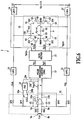
- the driving device 3 includes a driving circuit 20 outputting an output signal Vp-n2, an error suppression circuit 11 generating a first error suppression signal Vout1, a pulse width modulation circuit (PWM) 12 as a pulse modulation means outputting switching control signals Vp1 and Vp2 corresponding to pulse modulation signals, a gate driver 13, and low pass filters (LPF1, LPF2) 14 and 15 as a first feedback means.
- a driving circuit 20 outputting an output signal Vp-n2
- an error suppression circuit 11 generating a first error suppression signal Vout1
- PWM pulse width modulation circuit
- LPF1 LPF2 low pass filters
- the driving circuit 20 includes a switching circuit 100 having a plurality of switching elements 101, 102, 103 and 104, and inductive load L1 as the load is connected at terminals between connection points OUTP and OUTN.
- Each of the switching elements 101, 102, 103 and 104 i.e. transistors such as MOSFET
- the low pass filters (LPF1, LPF2) 14 and 15 feed back output signal Vp-n2 at the output terminals 50 and 51 of the driving circuit 20 to terminals 9a and 9b via feedback resistors RF1 and RF2 of the error suppression circuit 11.
- output signals V2a and V2b are used as the signals fed back.
- the error suppression circuit 11 is constructed as an integrator including a differential amplifier circuit 111, a capacitor C2 connected between terminals 9a and 10a, a capacitor C3 connected between terminals 9b and 10b, input resistors RS1 and RS2 connected between input terminals 8a and 9a and between input terminals 8b and 9b, respectively, and the feedback resistors RF1 and RF2 connected to the terminals 9a and 9b, respectively.
- the error suppression circuit 11 compare the amplitude of output signals V2a and V2b fed back via the low pass filters (LPF1, LPF2) 14 and 15 with the amplitude of input signal Vin inputted to the input terminals 8a and 8b, thus detecting an error of amplitude between signals. Then, a corrected voltage (i.e. first error suppression signal Vout1 is produced such that the detected error of amplitude between signals is suppressed.
- first error suppression signal Vout1 is produced such that the detected error of amplitude between signals is suppressed.
- continuous processing is performed but
- low pass filters (LPF3, LPF4) 16 and 17 are connected to the output terminals 50 and 51 of the driving circuit 20. Then, output signal Vp-n20 is produced from the output terminals 52 and 53 of the low pass filters (LPF3, LPF4) 16 and 17. In this case, these low pass filters (LPF3, LPF4) 16 and 17 are not necessitated structure elements in the driving device 3, and are no relationship with the operation as a switching amplifier.
- the circuit operation is as follows.
- the pulse width modulation circuit (PWM) 12 produces switching control signals Vp1 and VP2 based on the produced first error suppression signal Vout1. Then, the produced switching control signals Vp1 and VP2 are inputted via the gate driver 13 to the third terminal 42 of the switching elements 101, 102, 103 and 104, thus performing on/off behavior of the switching elements 101, 102, 103 and 104 to control supplying of a current I to the inductive load L1.
- PWM pulse width modulation circuit
- the pulse width modulation circuit (PWM) 12 includes a triangular wave generator 90 and two comparators 91a and 91b.
- the triangular wave generator 90 generates a triangular wave as a reference signal.
- the produced triangular wave is inputted as the comparison processing of the comparators 91a and 91b.
- the gate driver 13 includes two dead time generation circuits 92a and 92b, and two driving circuits 93a and 93b.
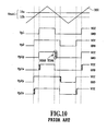
- FIG. 10 shows a timing chart of waveforms of various signals outputted from the pulse width modulation circuit (PWM) 12 and gate driver 13 shown in FIG. 9 .
- PWM pulse width modulation circuit
- the pulse width modulation circuit (PWM) 12 the first error suppression signal Vout1 outputted from the terminals 10a and 10b of the error suppression circuit 11 is compared with a triangular wave 302 being the reference signal, and pulse modulation signals Vp1 and Vp2 are outputted as the comparison result.
- pulse modulation signal Vp2 is inputted to the dead time generation circuit 92b, and the dead time generation circuit 92b delays the rise or fall time of pulse modulation signal Vp2 a dead time. Then, the delayed signal is buffered by the drive circuit 93b and outputted as switching control signals Vp2p and Vp2n.
- the transistors 103 and 104 are controlled based on switching control signals Vp2p and Vp2n.
- a non-overlap period (dead time) of about several ns to several 10 ns is inserted in pulse modulation signals Vp1 and Vp2, respectively.
- the number of output lines for switching control signals Vp1p, Vp1n, Vp2p and Vp2n become four.
- the pair of transistors 101 and 102, or the pair of transistors 103 and 104 performs on-behavior simultaneously at the moment when each signal varies, thus preventing large current from flowing from the power source to the ground.
- WO 01/71905 A2 relates to an amplifier circuit and method for providing negative feedback thereto.
- EP 1394934 A2 relates to a digital power amplifier.
- output signals V2a and V2b having distorted waveforms due to various error generation factors, such as rise delay of switching signal, fluctuations of power source voltage, and voltage error between the switching waveforms due to a mismatch between the on-resistances of the switching elements, are fed back to the terminals 9a and 9b. Then, an error component between this fed back output signals V2a and V2b and input signal Vin is detected by the error suppression circuit 11. That error is suppressed based on feedback loop gain, and first error suppression signal Vout1 is generated as the voltage in which the error is corrected. This first error suppression signal Vout1 is inputted to the pulse width modulation circuit (PWM) and processed.
- PWM pulse width modulation circuit
- FIG. 11 shows a variation of signal level of input signal waveform inputted to the pulse width modulation circuit (PWM) 12.
- PWM pulse width modulation circuit
- output signals V2a and V2b are fed back, whereby signal waveform distortion is suppressed by feedback loop gain.
- an object of the present invention is to provide a driving device which effectively suppresses distortion of signal waveform outputted by a switching amplifier and further can generate a signal waveform in which input reproducibility of output signal has been improved.
- a driving device for controlling electric power to load based on switching elements comprising:
- the second feedback means includes a differentiation circuit that differentiates a signal outputted from the error suppression means.
- the second feedback means additionally includes a high-pass filter or a band pass filter.
- the load is capacitive load or inductive load.
- the load is a piezoelectric speaker or a dynamic speaker.
- an information apparatus comprising: the driving device for controlling electric power to load based on the switching elements; an information processing portion, having a communication function and an information processing function, for controlling the driving device; and a battery for supplying electric power to the driving device and the information processing portion.
- the driving device is incorporated into an information apparatus for controlling electric power to load. Accordingly, the sound quality of a speaker can be highly improved, for example.
- FIGS. 1 to 5 A first embodiment of the present invention will be described with reference to FIGS. 1 to 5 .
- the same reference numerals are applied to the parts corresponding to those of FIG. 8 , and an explanation thereof is omitted.
- the driving device is constructed as a switching amplifier (class D amplifier) having inductive load such as a dynamic speaker as load.
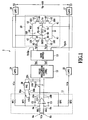
- FIG. 1 illustrates an exemplary configuration in which the driving device 1 used as a switching amplifier is provided with an arithmetic circuit 18 as a second feedback means.
- the driving device 1 includes a driving circuit 10 outputting an output signal Vp-n1, an arithmetic circuit 18 detecting an inclination of a first error suppression signal Vout1 to generate an inclination signal, an error suppression circuit 11 by which, when the inclination signal of first error suppression signal Vout1 is fed back, a second error suppression signal Vout2 can be further generated, a pulse width modulation circuit (PWM) 12 as a pulse modulation means outputting pulse modulation signals Vp1 and Vp2, a gate driver 13 outputting switching control signals Vp1p, Vp1n, Vp2p and Vp2n to respective switching elements 101, 102, 103 and 104 of the driving circuit 10, and low pass filters (LPF1, LPF2) 14 and 15 as a first feedback means.
- the error suppression circuit 11 is constructed as an integrator.
- the driving circuit 10 has a switching circuit 100 including a plurality of the switching elements 101, 102, 103 and 104; inductive load L1 as the load is connected at terminals between connection points OUTP and OUTN of the driving circuit 10.
- low pass filters (LPF3, LPF4) 16 and 17 are connected to the output terminals 50 and 51 of the driving circuit 10, for the sake of convenience, whereby an output signal Vp-n10 is extracted from output terminals 52 and 53 of the low pass filters (LPF3, LPF4) 16 and 17.
- these low pass filters (LPF3, LPF4) 16 and 17 are not necessitated structure elements in the driving device 1, and are no relationship with the operation as a switching amplifier.
- the arithmetic circuit 18 is connected between the error suppression circuit 11 and the pulse width modulation circuit (PWM) 12. Connection lines 19a and 19b on the input side is connected to an output line in which first error suppression signal Vout1 is outputted from the error suppression circuit 11. Connection lines 30a and 30b on the output side thereof are connected to resistors RF3 and RF4 of the error suppression circuit 11.
- PWM pulse width modulation circuit
- FIG. 2 shows a differentiation circuit as an example of the arithmetic circuit 18.
- the arithmetic circuit 18 includes a differential amplifier circuit 112, capacitors C4 and C5 connected between the input terminals 19a and 19b and the input terminals of the differential amplifier circuit 112 respectively, and resistors R1 and R2 connected between the input terminals and the output terminals 30a and 30b respectively.
- a differentiation signal containing this detected inclination is outputted.
- a detection signal Vfb2 containing the detected inclination is inputted to the error suppression circuit 11 together with fed back output signals V1a and V1b.
- output signals V1a and V1b containing the inclination of detection signal Vfb2 are compared with the inclination of input signal Vin.
- a second error suppression signal Vout2 is produced so that the inclination error between signals is suppressed.
- this input signal Vin may be a differential signal, or a single end that the input terminal 8a or 8b is connected to a reference signal level.
- the error suppression circuit 11 may be a single end configuration. In this case, OUTP and OUTN as differential output are changed to a single end and the output from the single end terminal may be fed back to the error suppression circuit 11.
- the driving circuit 10 may have a full-bridge configuration or a half-bridge configuration. In a half-bridge configuration, one terminal of the inductive load L1 is connected to the ground. In this case, the driving circuit 10 is comprised of two switching elements 101 and 102 (or 103 and 104).
- FIG. 3 is a flowchart explaining the basic circuit operation of the driving device 1.
- step S1 an output signal Vp-n1 at the output terminals 50 and 51 of the connection points between the terminals of the inductive load L1 and the first terminal 40 of the switching elements 101, 102, 103 and 104 is fed back as output signals V1a and V1b to the input terminals 9a and 9b via the low pass filters (LPF1, LPF2) 14 and 15.
- the voltage values of the fed back output signals V1a and V1b are accumulated across capacitors C2 and C3 of the differential amplifier circuit 111.
- step S2 the magnitude (amplitude) of the fed back output signals V1a and V1b is compared with the magnitude (amplitude) of input signal Vin to detect an error of magnitude (amplitude) between signals, and a first error suppression signal Vout1 is produced such that the detected error of amplitude between the signals is suppressed.
- step S4 the pulse width modulation circuit (PWM) 12 produce pulse modulation signals Vp1 and Vp2 having modulated pulse width based on the generated second error suppression signal Vout2.
- the produced pulse modulation signals Vp1 and Vp2 are inputted to the third terminal 42 of the switching elements 101, 102, 103 and 104 via the gate driver 13.
- the switching elements 101, 102, 103 and 104 perform on/off behavior to control supplying of a current I to the inductive load L1.
- detection signal Vfb2 is a signal produced by differentiating first error suppression signal Vout1 outputted from the arithmetic circuit 18.
- This output differentiation signal Vfb2 represents a variation of inclination of the first error suppression signal Vout1. As to the output, a steeper inclination becomes a larger variation.
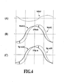
- FIG.4 show waveforms of various signals produced in each circuit portion of the driving device 1.
- output signal Vp-n1 outputted from the driving circuit 10 is inputted to the low pass filters 14 and 15 constituting the feedback circuit. Then, output signals V1a and V1b fed back via the low pass filters 14 and 15 is compared with input signal Vin. As a result, by using on a loop gain including the gain of the differential amplifier circuit 111, first error suppression signal Vout1 is produced.
- the first error suppression signal Vout1 is featured in that the error component is suppressed between the fed back output signals V1a and V1b and input signal Vin.
- This produced first error suppression signal Vout1 varies the duty ratio of switching control signals Vp1 and VP2 as pulse modulation signals, but a waveform error component which cannot be suppressed enough by the error suppression circuit 11 still remains.
- This error component contained in first error suppression signal Vout1 can be regarded as a difference between the inclination of output signal waveform and the inclination of input signal waveform.
- first error suppression signal Vout1 containing that difference of inclination component is sent to the arithmetic circuit 18 constituted of a differentiation circuit. Then, an output differentiation signal Vfb2 as the inclination component is inputted via the feedback resistors RF3 and RF4 to the error suppression circuit 11.
- the error suppression circuit 11 calculates a variation component of detection signal Vfb2 to output second error suppression signal Vout2.
- first error suppression signal Vout1 is a waveform without distortion
- second error suppression signal Vout2 becomes a waveform having a phase lead corresponding to the magnitude of variation of detection signal Vfb2 produced by first error suppression signal Vout1, and thus there is no variation in the waveform quality.
- first error suppression signal Vout1 When first error suppression signal Vout1 is distorted, as shown in (B) of FIG. 4 , in a way that the inclination becomes a smooth curve in a delayed manner around the peak in a direction where the signal waveform varies from the zero cross point to the peak. Then, a voltage level of detection signal Vfb2' shown in (A) of FIG. 4 raises corresponding to the steep inclination, as compared to the waveform of detection signal Vfb2 shown in (B) of FIG. 5 observed when there is no distortion.
- this detection signal Vfb2' is inputted to the error suppression circuit 11, the addition amount is large only at points where the inclination of signal waveform is steep. Thus, the inclination becomes a smooth curve only at the points where the inclination of signal waveform is steep. Then, second error suppression signal Vout2 is produced, as shown in (B) of FIG. 4 , thus improving a distortion waveform. Also, the error suppression circuit 11 corrects the signal level corresponding to the increment by the addition of detection signal Vfb2' is corrected via the first feedback means (low pass filters 14 and 15).
- first error suppression signal Vout1 is expressed as a x sin ( ⁇ t)
- detection signal Vfb2' is expressed as b x cos ( ⁇ t)
- second error suppression signal Vout2 being the corrected signal is expressed as r x sin ( ⁇ t + ⁇ )
- r ⁇ (a2 + b2)
- ⁇ tan -1 (b/a)
- second error suppression signal Vout2 is produced by the arithmetic circuit 18 as the second feedback means, thus correcting the waveform distortion at the inductive load L1 to improve the input reproducibility.
- the value of THD Total Harmonic Distortion
- THD In view of the frequency domain, distortion components are lowered totally in even-order and odd-order, thus improving THD up to about 80 dB. In comparison with THD of the switching amplifier of FIG. 8 as only the first feedback means, THD can be improved about 10 dB.
- a size of about 2 mm x 2 mm may be set in case that two channels are incorporated in switching amplifiers.
- a second embodiment of the present invention will be described with reference to FIG. 6 .
- the driving device is an example of a switching amplifier (class D amplifier) having capacitive load such as a piezoelectric speaker.
- a switching amplifier class D amplifier
- capacitive load such as a piezoelectric speaker.
- FIG. 6 shows an example in which a driving device 2 of a switching amplifier is provided with an arithmetic circuit 18 as a second feedback means.
- the driving circuit 10 has a switching circuit 100 including a plurality of switching elements 101, 102, 103 and 104. Capacitive load C1 as load is connected at terminals between connection points OUTP and OUTN of the driving circuit 10.
- step S2 the magnitude (amplitude) of the fed back output signals V1a and V1b is compared with the magnitude (amplitude) of input signal Vin to detect an error of magnitude (amplitude) between signals.
- a first error suppression signal Vout1 is produced such that the detected error of amplitude between the signals is suppressed.
- step S3 detection signal Vfb2 containing a inclination component of first error suppression signal Vout1, detected by the arithmetic circuit 18 as the second feedback means, is inputted via the resistors RF3 and RF4 to the error suppression circuit 11.
- a second error suppression signal Vout2 is produced such that the error due to the inclination component of input signal Vin is suppressed.
Landscapes
- Engineering & Computer Science (AREA)
- Power Engineering (AREA)
- Physics & Mathematics (AREA)
- Nonlinear Science (AREA)
- Amplifiers (AREA)
- Electronic Switches (AREA)
Claims (6)
- Dispositif d'attaque servant à commander la distribution d'énergie vers une charge (L1, C1) à partir d'éléments de commutation (101, 102, 103, 104), le dispositif comprenant :un moyen d'attaque (20) possédant un circuit de commutation (100) comportant une pluralité d'éléments de commutation (101, 102, 103, 104) reliés à la charge (L1, C1) ;un premier moyen de réinjection (14, 15) servant à réinjecter un signal de sortie au niveau d'une borne de sortie de la charge sur une borne d'entrée à laquelle un signal d'entrée est appliqué ;un moyen de suppression d'erreur (11) relié à la borne d'entrée, servant à produire un signal de suppression d'erreur (9a, 9b) ;un moyen de commande (12, 13) servant à commander la commutation du fonctionnement de la pluralité d'éléments de commutation (101, 102, 103, 104) dans le moyen d'attaque (20) à partir du signal de suppression d'erreur (9a, 9b) ; caractérisé parun deuxième moyen de réinjection (18) servant à détecter une composante de pente en différentiant un signal fourni par le moyen de suppression d'erreur (11) et à réinjecter la composante de pente sur une borne d'entrée du moyen de suppression d'erreur,dans lequel le moyen de suppression d'erreur compare le signal d'entrée à un signal de combinaison constitué par la composante de pente réinjectée par le deuxième moyen de réinjection à laquelle est ajouté le signal de sortie réinjecté par le premier moyen de réinjection afin de détecter une erreur d'amplitude entre les signaux, et produit le signal de suppression d'erreur dans lequel l'erreur a été corrigée.
- Dispositif d'attaque selon la revendication 1, dans lequel le deuxième moyen de réinjection (18) comporte un circuit de différentiation qui différentie un signal fourni par le moyen de suppression d'erreur.
- Dispositif d'attaque selon la revendication 1, dans lequel le deuxième moyen de réinjection (18) comporte en outre un filtre passe-haut ou un filtre passe-bas.
- Dispositif d'attaque selon l'une quelconque des revendications 1 à 3, dans lequel la charge est une charge capacitive (C1) ou une charge inductive (L1).
- Dispositif d'attaque selon l'une quelconque des revendications 1 à 3, dans lequel la charge est un haut-parleur piézoélectrique (C1) ou un haut-parleur dynamique (L1).
- Appareil d'information, comprenant :un dispositif d'attaque (204) selon l'une quelconque des revendications 1 à 5 qui commande la distribution d'énergie vers une charge à partir d'éléments de commutation (101, 102, 103, 104) ;une partie de traitement de l'information (202), possédant une fonction de communication et une fonction de traitement de l'information, servant à commander le dispositif d'attaque ; etune batterie (203) servant à alimenter en énergie électrique le dispositif d'attaque et la partie de traitement de l'information.
Applications Claiming Priority (3)
| Application Number | Priority Date | Filing Date | Title |
|---|---|---|---|
| JP2006135596 | 2006-05-15 | ||
| JP2007042485 | 2007-02-22 | ||
| PCT/JP2007/059946 WO2007132842A1 (fr) | 2006-05-15 | 2007-05-15 | Dispositif d'entraînement |
Publications (3)
| Publication Number | Publication Date |
|---|---|
| EP2019488A1 EP2019488A1 (fr) | 2009-01-28 |
| EP2019488A4 EP2019488A4 (fr) | 2013-02-27 |
| EP2019488B1 true EP2019488B1 (fr) | 2014-12-24 |
Family
ID=38693932
Family Applications (1)
| Application Number | Title | Priority Date | Filing Date |
|---|---|---|---|
| EP07743381.1A Ceased EP2019488B1 (fr) | 2006-05-15 | 2007-05-15 | Dispositif d'entraînement |
Country Status (5)
| Country | Link |
|---|---|
| US (1) | US7463090B2 (fr) |
| EP (1) | EP2019488B1 (fr) |
| JP (1) | JP4759050B2 (fr) |
| KR (1) | KR100977505B1 (fr) |
| WO (1) | WO2007132842A1 (fr) |
Families Citing this family (9)
| Publication number | Priority date | Publication date | Assignee | Title |
|---|---|---|---|---|
| CN101443998B (zh) * | 2006-05-15 | 2011-05-04 | 旭化成电子材料元件株式会社 | 驱动装置 |
| TWI353718B (en) * | 2007-12-25 | 2011-12-01 | Anpec Electronics Corp | Switching amplifier |
| US7999610B2 (en) * | 2009-11-11 | 2011-08-16 | Amazing Microelectronic Corp. | Class D amplifier capable of setting restraint power |
| KR20130006424A (ko) * | 2009-11-30 | 2013-01-16 | 에스티 에릭슨 에스에이 | 디바이스 내의 팝업 노이즈 감소 |
| TWI411224B (zh) * | 2009-12-07 | 2013-10-01 | Faraday Tech Corp | D級放大器 |
| JP5324417B2 (ja) * | 2009-12-25 | 2013-10-23 | 旭化成エレクトロニクス株式会社 | 駆動用ドライバ、駆動用アンプおよび情報機器 |
| US9000690B2 (en) | 2012-06-13 | 2015-04-07 | Texas Instruments Incorporated | Driver for capacitive loads |
| DK201770859A1 (en) * | 2016-11-14 | 2018-05-28 | Tymphany Hk Ltd | Class-d power amplifier nested inside low-noise differential op-amp feedback loop |
| US12255436B2 (en) * | 2020-12-16 | 2025-03-18 | Macom Technology Solutions Holdings, Inc. | PAM driver with distributed modulation current setpoint feedback |
Family Cites Families (16)
| Publication number | Priority date | Publication date | Assignee | Title |
|---|---|---|---|---|
| JPH0728181B2 (ja) * | 1988-12-28 | 1995-03-29 | パイオニア株式会社 | パルス幅変調増幅回路 |
| US5672998A (en) * | 1995-08-09 | 1997-09-30 | Harris Corporation | Class D amplifier and method |
| US5805020A (en) * | 1996-06-27 | 1998-09-08 | Harris Corporation | Silent start class D amplifier |
| US6229389B1 (en) * | 1998-11-18 | 2001-05-08 | Intersil Corporation | Class D modulator with peak current limit and load impedance sensing circuits |
| US6262632B1 (en) | 1999-11-16 | 2001-07-17 | Texas Instruments Incorporated | Concept and method to enable filterless, efficient operation of Class-D amplifiers |
| US6211728B1 (en) * | 1999-11-16 | 2001-04-03 | Texas Instruments Incorporated | Modulation scheme for filterless switching amplifiers |
| US6441685B1 (en) * | 2000-03-17 | 2002-08-27 | Jl Audio, Inc. | Amplifier circuit and method for providing negative feedback thereto |
| US6614297B2 (en) * | 2001-07-06 | 2003-09-02 | Texas Instruments Incorporated | Modulation scheme for filterless switching amplifiers with reduced EMI |
| JP3499236B1 (ja) | 2002-08-28 | 2004-02-23 | 株式会社フライングモール | ディジタル電力増幅器 |
| JP3776392B2 (ja) * | 2002-10-03 | 2006-05-17 | 三菱電機株式会社 | D級増幅器 |
| JP4770292B2 (ja) * | 2004-07-02 | 2011-09-14 | ヤマハ株式会社 | パルス幅変調増幅器 |
| JP2006060549A (ja) * | 2004-08-20 | 2006-03-02 | Yamaha Corp | ディジタルアンプ |
| JP4535819B2 (ja) * | 2004-09-24 | 2010-09-01 | Necアクセステクニカ株式会社 | 駆動回路および該駆動回路を備える携帯機器 |
| JP4515926B2 (ja) | 2005-01-24 | 2010-08-04 | 旭化成エレクトロニクス株式会社 | デジタルスイッチングアンプ |
| US7227408B2 (en) * | 2005-05-26 | 2007-06-05 | Bhc Consulting Pty., Ltd. | Low distortion class-D amplifier using sampling of a servo-loop amplifier output |
| US7355473B2 (en) | 2005-11-03 | 2008-04-08 | Amazion Electronics, Inc. | Filterless class D power amplifier |
-
2007
- 2007-05-15 KR KR1020087018270A patent/KR100977505B1/ko not_active Expired - Fee Related
- 2007-05-15 US US11/798,592 patent/US7463090B2/en not_active Expired - Fee Related
- 2007-05-15 JP JP2008515560A patent/JP4759050B2/ja not_active Expired - Fee Related
- 2007-05-15 EP EP07743381.1A patent/EP2019488B1/fr not_active Ceased
- 2007-05-15 WO PCT/JP2007/059946 patent/WO2007132842A1/fr not_active Ceased
Also Published As
| Publication number | Publication date |
|---|---|
| WO2007132842A1 (fr) | 2007-11-22 |
| KR20080090463A (ko) | 2008-10-08 |
| US7463090B2 (en) | 2008-12-09 |
| EP2019488A1 (fr) | 2009-01-28 |
| JPWO2007132842A1 (ja) | 2009-09-24 |
| EP2019488A4 (fr) | 2013-02-27 |
| JP4759050B2 (ja) | 2011-08-31 |
| KR100977505B1 (ko) | 2010-08-23 |
| US20070273437A1 (en) | 2007-11-29 |
Similar Documents
| Publication | Publication Date | Title |
|---|---|---|
| EP2019488B1 (fr) | Dispositif d'entraînement | |
| CN101443998B (zh) | 驱动装置 | |
| CN1941613B (zh) | D类放大器 | |
| CN102883242B (zh) | 多功能扬声器驱动控制装置及控制方法 | |
| US7446603B2 (en) | Differential input Class D amplifier | |
| US6788137B2 (en) | Switching amplifier and signal amplifying method | |
| US9444419B2 (en) | Boosted differential class H amplifier | |
| JP4535819B2 (ja) | 駆動回路および該駆動回路を備える携帯機器 | |
| US7948313B2 (en) | Class D amplifier circuit | |
| CN111585526B (zh) | 音频调制电路和电子设备 | |
| CN111628728A (zh) | 音频调制电路和电子设备 | |
| CN202586876U (zh) | 差频消除电路、脉冲宽度调制信号产生电路与放大器电路 | |
| CN111740713A (zh) | 音频调制方法 | |
| US10749486B2 (en) | Class D amplifier current feedback | |
| CN115769493A (zh) | 音频电路、使用其的电子设备及车载音频系统 | |
| US20060145755A1 (en) | Square wave modulation design for a class-D audio amplifier | |
| JP3132280B2 (ja) | D級電力増幅器 | |
| US11159132B2 (en) | Class D amplifier stereo to mono converter | |
| JP2004048333A (ja) | Pwm変調方式d級アンプ | |
| US20060125554A1 (en) | Asynchronous BTL design for a class-D audio amplifier | |
| US10284152B2 (en) | Amplifier, audio signal output method, and electronic device | |
| US11784615B2 (en) | Class-D amplifier with nested feedback loops | |
| CN2862500Y (zh) | 方波调制的d类音频放大器 | |
| US20250047249A1 (en) | Triangle wave generator circuit with noise reduction | |
| CN101989836B (zh) | 高效率音频放大器及其相关方法 |
Legal Events
| Date | Code | Title | Description |
|---|---|---|---|
| PUAI | Public reference made under article 153(3) epc to a published international application that has entered the european phase |
Free format text: ORIGINAL CODE: 0009012 |
|
| 17P | Request for examination filed |
Effective date: 20080923 |
|
| AK | Designated contracting states |
Kind code of ref document: A1 Designated state(s): AT BE BG CH CY CZ DE DK EE ES FI FR GB GR HU IE IS IT LI LT LU LV MC MT NL PL PT RO SE SI SK TR |
|
| AX | Request for extension of the european patent |
Extension state: AL BA HR MK RS |
|
| DAX | Request for extension of the european patent (deleted) | ||
| RBV | Designated contracting states (corrected) |
Designated state(s): GB |
|
| REG | Reference to a national code |
Ref country code: DE Ref legal event code: 8566 |
|
| A4 | Supplementary search report drawn up and despatched |
Effective date: 20130128 |
|
| RIC1 | Information provided on ipc code assigned before grant |
Ipc: H03K 5/06 20060101ALI20130122BHEP Ipc: H03K 7/08 20060101ALI20130122BHEP Ipc: H03K 17/687 20060101AFI20130122BHEP Ipc: H03K 17/284 20060101ALI20130122BHEP |
|
| GRAP | Despatch of communication of intention to grant a patent |
Free format text: ORIGINAL CODE: EPIDOSNIGR1 |
|
| RIC1 | Information provided on ipc code assigned before grant |
Ipc: H03K 17/284 20060101ALI20140630BHEP Ipc: H03K 5/06 20060101ALI20140630BHEP Ipc: H03K 17/687 20060101AFI20140630BHEP Ipc: H03K 7/08 20060101ALI20140630BHEP |
|
| INTG | Intention to grant announced |
Effective date: 20140716 |
|
| GRAS | Grant fee paid |
Free format text: ORIGINAL CODE: EPIDOSNIGR3 |
|
| GRAA | (expected) grant |
Free format text: ORIGINAL CODE: 0009210 |
|
| AK | Designated contracting states |
Kind code of ref document: B1 Designated state(s): GB |
|
| REG | Reference to a national code |
Ref country code: GB Ref legal event code: FG4D |
|
| PLBE | No opposition filed within time limit |
Free format text: ORIGINAL CODE: 0009261 |
|
| STAA | Information on the status of an ep patent application or granted ep patent |
Free format text: STATUS: NO OPPOSITION FILED WITHIN TIME LIMIT |
|
| 26N | No opposition filed |
Effective date: 20150925 |
|
| PGFP | Annual fee paid to national office [announced via postgrant information from national office to epo] |
Ref country code: GB Payment date: 20180329 Year of fee payment: 12 |
|
| GBPC | Gb: european patent ceased through non-payment of renewal fee |
Effective date: 20190515 |
|
| PG25 | Lapsed in a contracting state [announced via postgrant information from national office to epo] |
Ref country code: GB Free format text: LAPSE BECAUSE OF NON-PAYMENT OF DUE FEES Effective date: 20190515 |