EP2019575A2 - Vorrichtung und Verfahren zur Montage leitfähiger Kugeln, Maske für die Montage die leitfähiger Kugeln und Verfahren zur Herstellung der Maske - Google Patents
Vorrichtung und Verfahren zur Montage leitfähiger Kugeln, Maske für die Montage die leitfähiger Kugeln und Verfahren zur Herstellung der Maske Download PDFInfo
- Publication number
- EP2019575A2 EP2019575A2 EP08159779A EP08159779A EP2019575A2 EP 2019575 A2 EP2019575 A2 EP 2019575A2 EP 08159779 A EP08159779 A EP 08159779A EP 08159779 A EP08159779 A EP 08159779A EP 2019575 A2 EP2019575 A2 EP 2019575A2
- Authority
- EP
- European Patent Office
- Prior art keywords
- ball mounting
- conductive ball
- conductive
- mask
- portions
- Prior art date
- Legal status (The legal status is an assumption and is not a legal conclusion. Google has not performed a legal analysis and makes no representation as to the accuracy of the status listed.)
- Withdrawn
Links
Images


Classifications
-
- H—ELECTRICITY
- H05—ELECTRIC TECHNIQUES NOT OTHERWISE PROVIDED FOR
- H05K—PRINTED CIRCUITS; CASINGS OR CONSTRUCTIONAL DETAILS OF ELECTRIC APPARATUS; MANUFACTURE OF ASSEMBLAGES OF ELECTRICAL COMPONENTS
- H05K3/00—Apparatus or processes for manufacturing printed circuits
- H05K3/30—Assembling printed circuits with electric components, e.g. with resistors
- H05K3/32—Assembling printed circuits with electric components, e.g. with resistors electrically connecting electric components or wires to printed circuits
- H05K3/34—Assembling printed circuits with electric components, e.g. with resistors electrically connecting electric components or wires to printed circuits by soldering
- H05K3/3465—Application of solder
- H05K3/3478—Application of solder preforms; Transferring prefabricated solder patterns
-
- H—ELECTRICITY
- H10—SEMICONDUCTOR DEVICES; ELECTRIC SOLID-STATE DEVICES NOT OTHERWISE PROVIDED FOR
- H10W—GENERIC PACKAGES, INTERCONNECTIONS, CONNECTORS OR OTHER CONSTRUCTIONAL DETAILS OF DEVICES COVERED BY CLASS H10
- H10W72/00—Interconnections or connectors in packages
- H10W72/01—Manufacture or treatment
- H10W72/011—Apparatus therefor
- H10W72/0112—Apparatus for manufacturing bump connectors
-
- H—ELECTRICITY
- H05—ELECTRIC TECHNIQUES NOT OTHERWISE PROVIDED FOR
- H05K—PRINTED CIRCUITS; CASINGS OR CONSTRUCTIONAL DETAILS OF ELECTRIC APPARATUS; MANUFACTURE OF ASSEMBLAGES OF ELECTRICAL COMPONENTS
- H05K2203/00—Indexing scheme relating to apparatus or processes for manufacturing printed circuits covered by H05K3/00
- H05K2203/04—Soldering or other types of metallurgic bonding
- H05K2203/041—Solder preforms in the shape of solder balls
-
- H—ELECTRICITY
- H05—ELECTRIC TECHNIQUES NOT OTHERWISE PROVIDED FOR
- H05K—PRINTED CIRCUITS; CASINGS OR CONSTRUCTIONAL DETAILS OF ELECTRIC APPARATUS; MANUFACTURE OF ASSEMBLAGES OF ELECTRICAL COMPONENTS
- H05K2203/00—Indexing scheme relating to apparatus or processes for manufacturing printed circuits covered by H05K3/00
- H05K2203/04—Soldering or other types of metallurgic bonding
- H05K2203/0485—Tacky flux, e.g. for adhering components during mounting
-
- H—ELECTRICITY
- H05—ELECTRIC TECHNIQUES NOT OTHERWISE PROVIDED FOR
- H05K—PRINTED CIRCUITS; CASINGS OR CONSTRUCTIONAL DETAILS OF ELECTRIC APPARATUS; MANUFACTURE OF ASSEMBLAGES OF ELECTRICAL COMPONENTS
- H05K2203/00—Indexing scheme relating to apparatus or processes for manufacturing printed circuits covered by H05K3/00
- H05K2203/05—Patterning and lithography; Masks; Details of resist
- H05K2203/0548—Masks
- H05K2203/0557—Non-printed masks
-
- H—ELECTRICITY
- H05—ELECTRIC TECHNIQUES NOT OTHERWISE PROVIDED FOR
- H05K—PRINTED CIRCUITS; CASINGS OR CONSTRUCTIONAL DETAILS OF ELECTRIC APPARATUS; MANUFACTURE OF ASSEMBLAGES OF ELECTRICAL COMPONENTS
- H05K2203/00—Indexing scheme relating to apparatus or processes for manufacturing printed circuits covered by H05K3/00
- H05K2203/08—Treatments involving gases
- H05K2203/082—Suction, e.g. for holding solder balls or components
-
- H—ELECTRICITY
- H10—SEMICONDUCTOR DEVICES; ELECTRIC SOLID-STATE DEVICES NOT OTHERWISE PROVIDED FOR
- H10W—GENERIC PACKAGES, INTERCONNECTIONS, CONNECTORS OR OTHER CONSTRUCTIONAL DETAILS OF DEVICES COVERED BY CLASS H10
- H10W72/00—Interconnections or connectors in packages
- H10W72/01—Manufacture or treatment
- H10W72/012—Manufacture or treatment of bump connectors, dummy bumps or thermal bumps
- H10W72/01204—Manufacture or treatment of bump connectors, dummy bumps or thermal bumps using temporary auxiliary members, e.g. using sacrificial coatings or handle substrates
-
- H—ELECTRICITY
- H10—SEMICONDUCTOR DEVICES; ELECTRIC SOLID-STATE DEVICES NOT OTHERWISE PROVIDED FOR
- H10W—GENERIC PACKAGES, INTERCONNECTIONS, CONNECTORS OR OTHER CONSTRUCTIONAL DETAILS OF DEVICES COVERED BY CLASS H10
- H10W72/00—Interconnections or connectors in packages
- H10W72/01—Manufacture or treatment
- H10W72/012—Manufacture or treatment of bump connectors, dummy bumps or thermal bumps
- H10W72/01221—Manufacture or treatment of bump connectors, dummy bumps or thermal bumps using local deposition
- H10W72/01223—Manufacture or treatment of bump connectors, dummy bumps or thermal bumps using local deposition in liquid form, e.g. by dispensing droplets or by screen printing
-
- H—ELECTRICITY
- H10—SEMICONDUCTOR DEVICES; ELECTRIC SOLID-STATE DEVICES NOT OTHERWISE PROVIDED FOR
- H10W—GENERIC PACKAGES, INTERCONNECTIONS, CONNECTORS OR OTHER CONSTRUCTIONAL DETAILS OF DEVICES COVERED BY CLASS H10
- H10W72/00—Interconnections or connectors in packages
- H10W72/01—Manufacture or treatment
- H10W72/012—Manufacture or treatment of bump connectors, dummy bumps or thermal bumps
- H10W72/01221—Manufacture or treatment of bump connectors, dummy bumps or thermal bumps using local deposition
- H10W72/01225—Manufacture or treatment of bump connectors, dummy bumps or thermal bumps using local deposition in solid form, e.g. by using a powder or by stud bumping
-
- H—ELECTRICITY
- H10—SEMICONDUCTOR DEVICES; ELECTRIC SOLID-STATE DEVICES NOT OTHERWISE PROVIDED FOR
- H10W—GENERIC PACKAGES, INTERCONNECTIONS, CONNECTORS OR OTHER CONSTRUCTIONAL DETAILS OF DEVICES COVERED BY CLASS H10
- H10W72/00—Interconnections or connectors in packages
- H10W72/20—Bump connectors, e.g. solder bumps or copper pillars; Dummy bumps; Thermal bumps
- H10W72/251—Materials
Definitions
- the present invention relates to a conductive ball mounting apparatus, a conductive ball mounting method, a mask used for mounting conductive balls, and a mask manufacturing method. More particularly, the present invention relates to a conductive ball mounting apparatus for mounting one conductive ball on each of a plurality of pads coated with an adhesive flux formed on a substrate such as a wiring substrate or a semiconductor wafer, a conductive ball mounting method, a mask used for mounting conductive balls, and a mask manufacturing method.
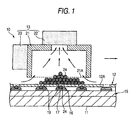
- FIG 1 is a sectional view of a conductive ball mounting apparatus in the related art.
- FIG 1 shows a conductive ball mounting apparatus 10 mounting each of conductive balls 24 on each of a plurality of pads 17 formed on a substrate 15.
- the conductive ball mounting apparatus 10 in the related art includes a stage 11, a conductive ball mounting mask 12, and a conductive ball supplying unit 13.
- the stage 11 is configured to hold the substrate 15 having the plurality of pads 17 coated with a flux 16.
- the conductive ball mounting mask 12 is disposed over the substrate 15 such that the conductive ball mounting mask 12 is stretched by a certain tension in the horizontal direction (a state that the conductive ball mounting mask 12 is not caused to bend).
- the conductive ball mounting mask 12 has a plurality of ball mounting through holes 19 that are used to mount each of the conductive balls 24 on each of the plurality of pads 17 (pads on which the flux 16 is coated).
- the conductive ball supplying unit 13 has a suction head 21, a sucking unit 22, and a driving unit 23.
- the suction head 21 has an inlet port 21 A.
- the suction head 21 is disposed over the conductive ball mounting mask 12 such that the inlet port 21 A opposes to the conductive ball mounting mask 12.
- the sucking unit 22 is driven, the suction head 21 collects the plurality of conductive balls 24, which are supplied onto the conductive ball mounting mask 12, on a portion of the conductive ball mounting mask 12 opposing to the suction head 21.
- the sucking unit 22 is provided on the suction head 21.
- the sucking unit 22 sucks the portion of the conductive ball mounting mask 12 opposing to the inlet port 21A (upper surface 12A side of the conductive ball mounting mask 12) via the inlet port 21A.
- the driving unit 23 is provided to the suction head 21.
- the driving unit 23 moves the suction head 21 in the direction that is parallel with the upper surface 12A of the conductive ball mounting mask 12.
- the conductive ball supplying unit 13 mounts each of the conductive balls 24 on each of the plurality of pads 17 (pads on which the flux 16 is coated) by moving the suction head 21 and the plurality of conductive balls 24 in the direction that is parallel with the upper surface 12A of the conductive ball mounting mask 12, while collecting the plurality of conductive balls 24, which are supplied onto the upper surface 12A of the conductive ball mounting mask 12, on the portion of the upper surface 12A of the conductive ball mounting mask 12 opposing to the inlet port 21A of the suction head 21 ( see e.g., JP-A-2006-73999 ).
- FIG2 is a view to describe disadvantages when each of the conductive balls is mounted on each of the pads using the conductive ball mounting apparatus in the related art.
- the same reference symbols are affixed to the same constituent portions as those of the structure shown in FIG 1 .
- the conductive ball mounting mask 12 is lifted up from a certain position by a sucking force generated by the conductive ball supplying unit 13. In this manner, when the conductive ball mounting mask 12 is lifted up from the certain position, other balls 24 fall through the ball mounting through holes 19 positioned over the pads 17 on which each of the conductive balls 24 is mounted. As a result, such a problem existed that the mounting position of the conductive balls 24 mounted on the pads 17 is displaced from a desired position, or such a problem existed that the plurality of conductive balls 24 are mounted on each of the pads 17.
- a conductive ball mounting apparatus includes: a conductive ball mounting mask disposed to oppose a substrate having a plurality of pads coated with an adhesive flux, the conductive ball mounting mask having a plurality of ball mounting through holes for mounting each of conductive balls on each of the plurality of pads, the plurality of ball mounting through holes being arranged to oppose to the plurality of pads; and a conductive ball supplying unit for moving or removing the conductive balls on the conductive ball mounting mask by sucking an air on an upper surface side of the conductive ball mounting mask.
- the conductive ball mounting mask includes through portions formed to block passing of the conductive balls.
- the portion of the conductive ball mounting mask being disposed over the pads on which the conductive ball is mounted respectively is never lifted up from a certain position.
- one conductive ball can be mounted on each of the plurality of pads without fail.
- the through portions may be configured to perform a ventilation of an air between an upper space and a lower space of the conductive ball mounting mask by a suction generated by the conductive ball supplying unit.
- a pressure difference between the upper space and the lower space of the conductive ball mounting mask can be reduced. As a result, such a situation can be prevented that the conductive ball mounting mask is lifted up from a certain position.
- the through portions are disposed near the plurality of ball mounting through holes.
- the conductive ball mounting mask is formed like a thin plate, and has a plate body in which the plurality of ball mounting through holes and the through portions are formed, and supporting portions for supporting the plate body and contacting the substrate.
- a relative displacement of the ball mounting through holes corresponding to the plurality of pads can be reduced.
- the conductive ball can be mounted in given positions on the plurality of pads with good precision respectively.
- the conductive ball mounting mask may be made of silicon.
- the silicon is used as the material of the conductive ball mounting mask, a deformation of the thinned silicon plate produced by an external force is smaller than the metallic foil. Therefore, when the conductive ball mounting mask is stretched in the horizontal direction by a certain tension to restrict its position, a relative displacement of the ball mounting through holes from the plurality of pads can be reduced. As a result, the conductive ball is mounted in given positions on the plurality of pads with good precision respectively.
- the conductive ball mounting method includes:
- the through portions may be disposed near the plurality of ball mounting through holes.
- the conductive ball mounting mask in a conductive ball mounting mask disposed to oppose a substrate having a plurality of pads coated with an adhesive flux, includes:
- the through portions may be disposed near the plurality of ball mounting through holes.
- the method includes:
- the conductive ball mounting mask made of silicon substrate can be manufactured.
- FIG3 is a sectional view of a conductive ball mounting apparatus according to an embodiment of the present invention.
- FIG3 shows a state that conductive balls 105 are mounted on a plurality of pads 112 formed on a substrate 101 using a conductive ball mounting apparatus 100 of the present embodiment.
- the conductive ball mounting apparatus 100 of the present embodiment includes a stage 102 for holding the substrate 101 thereon, a conductive ball mounting mask 103, and a conductive ball supplying unit 104.
- FIG4 is a plan view of the substrate 101 shown in FIG3 .
- illustration of an adhesive flux 115 shown in FIG.3 is omitted from FIG4 .
- the substrate 101 is configured to be divided into many pieces and a substrate 108 is formed in each of substrate forming areas A of a substrate main body 107.
- a plurality of substrates 108 are formed integrally in the substrate 101.
- the plurality of substrates 108 are divided into individual pieces by cutting the substrate 101 along cutting positions B.
- a wiring substrate (concretely, e.g., interposer), a semiconductor chip such as IC, LSI, or the like can be taken as an example.
- a wiring substrate concretely, e.g., interposer
- a semiconductor chip such as IC, LSI, or the like
- following explanation will be made by taking as an example the case where the wiring substrate is used as the substrate 108.
- the substrate 108 includes the substrate main body 107, through electrodes 111, pads 112, 116, solder resists 113, 117, and the adhesive fluxs 115.
- the substrate main body 107 is used to form the through electrodes 111, the pads 112, 116, and the solder resists 113, 117.
- a glass epoxy resin can be employed as the material of the substrate main body 107.
- the through electrode 111 is provided to pass through the portion of the substrate main body 107 positioned between the pad 112 and the pad 116. One end portion of the through electrode 111 is connected to the pad 112, and the other end portion is connected to the pad 116.
- the through electrode 111 is provided to connect electrically the pad 112 and the pad 116.
- the material of the through electrode 111 for example, Cu can be employed.
- the pad 112 is provided in plural on a surface 107A of the substrate main body 107 (surface of the substrate main body 107 on the side on which the conductive balls 105 are mounted) in a pad forming area C.
- the pad 112 provides a pad on which the conductive ball 105 serving as an external connection terminal of the substrate 108 is mounted.
- a Cu/Ni/Au laminated film formed by forming sequentially a Cu film, a Ni film, and an Au film on the surface 107A of the substrate main body 107 a Cu/Pd/Ni/Au laminated film formed by forming sequentially a Cu film, a Pd film, a Ni film, and an Au film on the surface 107A of the substrate main body 107 can be employed.
- the solder resist 113 has openings 119 from which areas in which the conductive ball 105 is disposed on the pad 112 are exposed.
- the solder resist 113 is provided on the surface 107A of the substrate main body 107 to cover the outer peripheral portions of the pads 112.
- the adhesive flux 115 is coated on each of the plurality of pads 112 exposed from the openings 119.
- the adhesive flux 115 is coated to secure temporarily the conductive ball 105 to the pad 112.
- the adhesive flux 115 for example, the flux, the solder paste, or the like can be used.
- the pads 116 are provided on a surface 107B of the substrate main body 107 (surface of the substrate main body 107 on the opposite side to the surface 107A of the substrate main body 107).
- the pads 116 provides a pad on which an electronic component (for example, passive component, active component or semiconductor chip such as IC or LSI) is mounted.
- a Cu/Ni/Au laminated film formed by forming sequentially a Cu film, a Ni film, and an Au film on the surface 107B of the substrate main body 107 a Cu/Pd/Ni/Au laminated film formed by forming sequentially a Cu film, a Pd film, a Ni film, and an Au film on the surface 107B of the substrate main body 107 can be employed.
- the solder resist 117 has openings 121 from which areas on which the electronic component (not shown) is mounted are exposed.
- the solder resist 117 is provided on the surface 107B of the substrate main body 107 to cover a part of the pads 116.
- the substrates 108 constructed as above are held on the stage 102 such that the plurality of pads 112 coated with the adhesive flux 115 are opposed to the conductive ball mounting mask 103.
- the stage 102 is used to hold the substrate 101, and is disposed under the conductive ball supplying unit 104.
- the conductive ball supplying unit 104 has a suction head 131, a sucking unit 132, and a driving unit 133.
- the suction head 131 has a cylinder portion 135, and a plate portion 136 provided to the upper end of the cylinder portion 135.
- the cylinder portion 135 has an inlet port 137 at the end portion on the opposite side to the side on which the plate portion 136 is provided.
- a clearance between a lower end of the cylinder portion 135 and an upper surface 103A of the conductive ball mounting mask 103 should be formed larger than a diameter of the conductive ball 105.
- the plate portion 136 has an opening 139 connected to the sucking unit 132. This opening 139 provides an opening that allows an air kept under the suction head 131 to pass through the sucking unit 132.
- the sucking unit 132 is provided on the plate portion 136.
- the sucking unit 132 sucks an air located in vicinity of the upper surface 103A, which opposes to the inlet port 137, of the conductive ball mounting mask 103 via the opening 139. Therefore, the sucking unit 132 collects a plurality of conductive balls 105 in a certain area (concretely, an area of the conductive ball mounting mask 103 opposing to the inlet port 137) of the conductive ball mounting mask 103 (in a state shown in FIG3 ).
- the driving unit 133 is provided to the suction head 131.
- the driving unit 133 mounts the conductive ball 105 on each of a plurality of pads 112 by moving the suction head 131 in the direction parallel with the upper surface 103A of the conductive ball mounting mask 103 while the sucking unit 132 is sucking an air located in vicinity of the upper surface 103A of the conductive ball mounting mask 103.
- the conductive ball supplying unit 104 constructed as above moves or removes a plurality of conductive balls 105 on the conductive ball mounting mask 103 by sucking the upper surface side of the conductive ball mounting mask 103, whereby the conductive ball 105 is mounted on each of the plurality of pads 112.
- the conductive ball mounting mask 103 is disposed on the substrate 101, and has a plate body 125 shaped like a thin plate, and supporting portions 126.
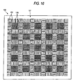
- FIG.5 is a plan view of the conductive ball mounting mask shown in FIG.3
- FIG6 is a plan view of the conductive ball mounting mask disposed on the substrate.
- the plate body 125 has a plurality of ball mounting through holes 128 and a plurality of through portions 129.
- the plurality of ball mounting through holes 128 are formed to pass through the plate body 125.
- the plurality of ball mounting through holes 128 are disposed to correspond to any one of the plurality of pads 112 provided on the substrate.
- the plurality of ball mounting through holes 128 are used to mount one conductive ball 105 on each of the plurality of pads 112.
- a diameter of the ball mounting through hole 128 can be set to 1.1 to 1.7 times as large as a diameter of the conductive ball 105, for example.
- the conductive ball 105 for example, either a solid sphere made of conductive material (e.g., Pb, Sn, Au, Ag, W, Ni, Mo, Al, or the like) or a solid sphere formed by coating a core made of resin with the conductive material can be employed. Also, a diameter of the conductive ball 105 can be set to 50 ⁇ m to 100 ⁇ m, for example.
- conductive material e.g., Pb, Sn, Au, Ag, W, Ni, Mo, Al, or the like
- a diameter of the conductive ball 105 can be set to 50 ⁇ m to 100 ⁇ m, for example.
- the through portion 129 is formed in plural to pass through the conductive ball mounting mask 103.
- the through portions 129 serve as air vent portions that perform the ventilation of an air between an upper space and a lower space of the conductive ball mounting mask 103.
- the through portions 129 are shaped to block the passing of the conductive ball 105.
- a plane shape of the through portion 129 can be set to a circle, for example (see FIG.5 and FIG6 ). Also, when a shape of the through portion 129 is set to a circle when viewed from a top, a diameter of the through portion 129 can be set to 0.05 to 0.9 times as large as a diameter of the conductive ball 105, for example.
- the through portions 129 constructed as above are formed in the portions of the plate body 125 opposing to the pad forming areas C of the substrate 101, and the portions of the plate body 125 opposing to the areas of the substrate 101 except the pad forming areas C (in other words, the portions of the plate body 125 positioned near the ball mounting through holes 128).
- each of the conductive balls 105 is mounted on each of the plurality of pads 112 by collecting the plurality of conductive balls 105 on the conductive ball mounting mask 103 by a sucking force and also by moving the plurality of conductive balls 105 in the direction parallel with the upper surface 103A of the conductive ball mounting mask 103. Accordingly, the portion of the conductive ball mounting mask 103 being disposed over the pads 112 on which each of the conductive balls 105 is mounted is never lifted up from a certain position. As a result, one conductive ball 105 can be mounted surely on each of the plurality of pads 112 coated with the adhesive flux 115.
- the through portions 129 for performing the ventilation of an air between the upper space and the lower space of the conductive ball mounting mask 103 are provided in the portions of the plate body 125 opposing to the areas of the substrate 101 except the pad forming areas C.
- the through portions 129 may be provided only in the portion of the plate body 125 opposing to the pad forming area C of the substrate 101.
- the plate body 125 constructed as above is stretched by a certain tension in the direction parallel with an upper surface 102A of the stage 102 such that the plate body 125 is not bended.
- a thickness of the plate body 125 can be set to 50 ⁇ m, for example.
- the case where the shape of the through portion 129 when viewed from the top is a circle is illustrated as an example.
- the shape of the through portion 129 is not limited to a circle, and any shape may be employed if such shape can block the passing of the conductive ball 105.
- a shape of the through portion 129 when viewed from a top for example, ellipse, triangle, quadrangle, polygon, or cross may be employed.
- the supporting portions 126 are provided on the lower surface side of the plate body 125.
- the supporting portions 126 are formed integrally with the plate body 125.
- the supporting portions 126 are supporting members that support the plate body 125 while contacting the solder resist 113 provided on the substrate 101.
- a height of the supporting portions 126 can be set to 50 ⁇ m, for example.
- each of the conductive balls 105 can be mounted in certain positions on each of the plurality of pads 112 (e.g., center positions of the plurality of pads 112) with good precision.
- the material of the conductive ball mounting mask 103 for example, metal (metallic foil), or a silicon can be used, but it is advantageous that a silicon should be used.
- a deformation of the silicon plate generated by an external force, when shaped into a thin plate, is smaller than that of the metallic foil. For this reason, for example, when the conductive ball mounting mask 103 is stretched in the horizontal direction by a certain tension to restrict its position, a relative displacement of the ball mounting through holes 128 with respect to the plurality of pads 112 can be reduced.
- the conductive ball 105 can be mounted in certain positions on each of the plurality of pads 112 (e.g., center positions of the pads 112) with good precision.
- insulating film e.g., oxide film, nitride film, or the like
- metal film e.g., Ni film, Au film, Cu film, Ti film, Cr film, or the like
- the metal film is provided on the surface of the conductive ball mounting mask 103 using the silicon as the base material, it can be prevented that the conductive ball mounting mask 103 is charged.
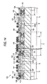
- FIG 7 to FIG 12 are views showing steps of manufacturing the conductive ball mounting mask when the conductive ball mounting mask is manufactured using the silicon substrate.
- the same reference symbols are affixed to the same constituent portions as those of the conductive ball mounting mask 103 shown in FIG.3 .
- a method of manufacturing the conductive ball mounting mask 103 when the silicon substrate is used as a base material will be described with reference to FIG7 to FIG 12 hereunder.
- a silicon substrate 141 shaped into a thin plate is prepared (silicon substrate preparing step).
- a silicon wafer e.g., a thickness is 725 ⁇ m
- a silicon wafer is polished until its thickness is reduced to 100 ⁇ m, and thus the silicon substrate 141 shaped into the thin plate is formed.
- a resist film 142 having first openings 144 and second openings 145 is formed on the silicon substrate 141 (resist film forming step).
- the first openings 144 are formed to expose the portions of an upper surface of the silicon substrate 141 corresponding to areas in which the ball mounting through holes 128 are formed
- the second openings 145 are formed to expose the portions of an upper surface of the silicon substrate 141 corresponding to areas in which the through portions 129 are formed.
- a diameter of the first opening 144 can be set to 1.1 to 1.7 times as large as a diameter of the conductive ball 105, for example.
- a diameter of the second opening 145 can be set to 0.05 to 0.9 times as large as a diameter of the conductive ball 105, for example.
- the plurality of ball mounting through holes 128 and the plurality of through portions 129 are formed simultaneously by etching the portions of the silicon substrate 141 by applying the anisotropic etching (e.g., dry etching using a gas such as SF 6 ) using the resist film 142 as a mask (ball mounting through hole and through portion forming steps). Accordingly, the plate body 125 having the plurality of ball mounting through holes 128 and the plurality of through portions 129 is manufactured.
- anisotropic etching e.g., dry etching using a gas such as SF 6
- the steps of manufacturing the conductive ball mounting mask 103 can be simplified in contrast to the case where the plurality of ball mounting through holes 128 and the plurality of through portions 129 are formed separately. Further, accuracy of position of the plurality of ball mounting through holes 128 and the plurality of through portions 129 can be improved.
- a resist film 161 is formed on portions of the lower surface of the silicon substrate 141 corresponding to areas in which the supporting portions 126 are formed, and then the supporting portions 126 are formed by etching the silicon substrate 141 by applying the anisotropic etching using the resist film 161 as a mask.
- the resist film 161 shown in FIG 11 is removed. Accordingly, the conductive ball mounting mask 103 using the silicon substrate 141 as the base material is manufactured.
- the resist film 142 having the first openings 144, which expose the portions of the silicon substrate 141 corresponding to the areas in which the plurality of ball mounting through hole 128 are formed, and the second openings 145, which expose the portions of the silicon substrate 141 corresponding to the areas in which the through portions 129 are formed, is formed on the silicon substrate 141 shaped into a thin plate. Then, the plurality of ball mounting through holes 128 and the plurality of through portions 129 are formed simultaneously by the anisotropic etching using the resist film 142 as a mask. Then, the resist film 142 is removed. Then, the resist film 161 is formed on the lower surface of the portions of the silicon substrate 141 corresponding to the forming areas of the supporting portions 126.
- the supporting portions 126 are formed by etching the silicon substrate 161 by applying the anisotropic etching using the resist film 142 as a mask.
- the conductive ball mounting mask 103 using the silicon substrate 141 as the base material is manufactured.
- the through portions 129 that perform the ventilation of an air between an upper space and a lower space of the conductive ball mounting mask 103 by a sucking force generated by the sucking unit 132 but prevent the passing of the conductive ball are provided in the conductive ball mounting mask 103 that has the plurality of ball mounting through holes 128 through which each of the conductive balls 105 is mounted on each of the plurality of pads 112 coated with the adhesive flux 115. Therefore, the portion of the conductive ball mounting mask 103 disposed over the pads 112 on which each of the conductive balls 105 is mounted is never lifted up from a certain position. As a result, one conductive ball 105 can be mounted without fail on each of the plurality of pads 112.
- FIGS.13 to 15 are views to describe an example of the conductive ball mounting method according to the embodiment of the present invention.
- the same reference symbols are affixed to the same constituent portions as those of the structure shown in FIG 3 .
- the conductive ball mounting mask 103 having the plurality of ball mounting through hole 128, which are used to mount one conductive ball 105 on each of the plurality of pads 112, and the through portions 129, which are formed to block the passing of the conductive ball 105, is disposed over the substrate 101 to oppose to this substrate (conductive ball mounting mask arranging step).
- the plurality of conductive balls 105 are supplied onto the conductive ball mounting mask 103 disposed in a certain position on the substrate 101 that is held on the stage 102 (conductive ball supplying step). At this time, the conductive balls 105 are mounted on a part of the plurality of pads 112.
- the plurality of conductive balls 105 are moved in the direction that is parallel with the upper surface 103A of the conductive ball mounting mask 103, while collecting the plurality of conductive balls 105 being fed onto the conductive ball mounting mask 103 in a certain area of the conductive ball mounting mask 103 (concretely, the portion of the conductive ball mounting mask 103 opposing to the inlet port 137) by sucking an air from the upper surface 103 side of the conductive ball mounting mask 103 (conductive ball moving step). Accordingly, in the conductive ball supplying step, one conductive ball 105 is mounted on all pads 112, on which the conductive ball 105 was not mounted.
- the method of mounting the conductive ball of the present embodiment while collecting the plurality of conductive ball 105 being fed onto the conductive ball mounting mask 103 on the portion of the conductive ball mounting mask 103 opposing to the inlet port 137, these conductive ball 105 are moved in the direction that is parallel with the upper surface 103A of the conductive ball mounting mask 103 by sucking the upper surface 103A side of the conductive ball mounting mask 103 in which the plurality of ball mounting through holes 128 and the through portions 129 being formed to block the passing of the conductive ball 105 are provided. Therefore, the portion of the conductive ball mounting mask 103 being disposed over the pads 112 on which each of the conductive balls 105 is mounted is never lifted up from a certain position. As a result, one conductive ball 105 can be mounted on each of the plurality of pads 112 without fail.
- FIG 16 is a plan view showing a variation of the conductive ball mounting mask. The illustration of the supporting portions 126 is omitted herein.
- the conductive ball mounting mask 150 is constructed similarly to the conductive ball mounting mask 103 except that a plate body 151 is provided instead of the plate body 125 that is provided to the conductive ball mounting mask 103 described in FIG.3 and FIG.5 .
- the plate body 151 has a plurality of ball mounting through holes 12 and through portions 152.
- the through portion 152 is a through slot (slit) formed to pass through the plate body 151, and the plurality of through portions 152 are formed in the plate body 151.
- the through portions 152 serve as the air vent ports that perform the ventilation of an air between an upper space and a lower space of the conductive ball mounting mask 150.
- the through portions 152 have a size (shape) that can block the passing of the conductive balls 105.
- a width of the through portion 152 when viewed from the top can be set to 0.05 to 0.9 times as large as a diameter of the conductive ball 105, for example.
- the through portions 129 are formed in the portions of the plate body 151 opposing to the pad forming areas C of the substrate 101 (in other words, the portions of the plate body 151 positioned near the ball mounting through holes 128), and the portions of the plate body 151 opposing to the areas of the substrate 101 except the pad forming areas C.
- a thickness of the plate body 151 can be set to 50 ⁇ m, for example.
- each of the conductive balls 105 is mounted on each of a plurality of pads 112 using the conductive ball mounting mask 103 shown in FIG.5 .
- the conductive ball 105 may be mounted on each of the plurality of pads 112 by providing the conductive ball mounting mask 150 shown in FIG 16 to the conductive ball mounting apparatus 100 instead of the conductive ball mounting mask 103.
- the similar advantages to the case where the conductive ball mounting mask 103 is used can be achieved.
- the through portion 152 may be provided only in the portions of the plate body 125 opposing to the pad forming areas C of the substrate 101.
- the conductive ball mounting mask 103 or 150 described in the present embodiment may be applicable to the conductive ball mounting apparatus including a ball recovering means that recovers the unnecessary conductive balls 105 not mounted on the pads 112 by the suction.
- the present invention is applicable to the conductive ball mounting apparatus for mounting one conductive ball on each of the plurality of pads coated with the adhesive flux on the substrate such as the wiring substrate or the semiconductor wafer, the conductive ball mounting method, the mask used for mounting conductive balls, and the mask manufacturing method.
Landscapes
- Engineering & Computer Science (AREA)
- Manufacturing & Machinery (AREA)
- Microelectronics & Electronic Packaging (AREA)
- Electric Connection Of Electric Components To Printed Circuits (AREA)
Applications Claiming Priority (1)
| Application Number | Priority Date | Filing Date | Title |
|---|---|---|---|
| JP2007176328A JP4430693B2 (ja) | 2007-07-04 | 2007-07-04 | 導電性ボール載置装置、導電性ボールの載置方法、導電性ボール載置用マスク、及びその製造方法 |
Publications (2)
| Publication Number | Publication Date |
|---|---|
| EP2019575A2 true EP2019575A2 (de) | 2009-01-28 |
| EP2019575A3 EP2019575A3 (de) | 2010-06-02 |
Family
ID=39916623
Family Applications (1)
| Application Number | Title | Priority Date | Filing Date |
|---|---|---|---|
| EP08159779A Withdrawn EP2019575A3 (de) | 2007-07-04 | 2008-07-04 | Vorrichtung und Verfahren zur Montage leitfähiger Kugeln, Maske für die Montage die leitfähiger Kugeln und Verfahren zur Herstellung der Maske |
Country Status (3)
| Country | Link |
|---|---|
| US (1) | US7866534B2 (de) |
| EP (1) | EP2019575A3 (de) |
| JP (1) | JP4430693B2 (de) |
Families Citing this family (9)
| Publication number | Priority date | Publication date | Assignee | Title |
|---|---|---|---|---|
| JP5453636B2 (ja) * | 2009-11-30 | 2014-03-26 | 澁谷工業株式会社 | 導電性ボールの搭載装置 |
| JP5639360B2 (ja) * | 2009-12-21 | 2014-12-10 | アスリートFa株式会社 | ボール誘導装置、ボール誘導方法およびボール搭載装置 |
| KR102100867B1 (ko) * | 2013-06-26 | 2020-04-14 | 삼성전자주식회사 | 솔더 볼 탑재 장치 |
| US9120170B2 (en) * | 2013-11-01 | 2015-09-01 | Zen Voce Corporation | Apparatus and method for placing and mounting solder balls on an integrated circuit substrate |
| JP6320066B2 (ja) * | 2014-02-13 | 2018-05-09 | イビデン株式会社 | ボール搭載用マスクおよびボール搭載装置 |
| JP6381322B2 (ja) * | 2014-07-07 | 2018-08-29 | マクセルホールディングス株式会社 | 配列用マスク |
| KR102472710B1 (ko) * | 2018-06-05 | 2022-11-30 | 쑤저우 레킨 세미컨덕터 컴퍼니 리미티드 | 반도체 소자 패키지 |
| KR102078935B1 (ko) * | 2018-11-07 | 2020-02-19 | 주식회사 프로텍 | 도전성 볼 탑재 장치 |
| KR102817428B1 (ko) * | 2022-07-05 | 2025-06-10 | 주식회사 프로텍 | 도전성 볼 탑재용 헤드 조립체 |
Citations (2)
| Publication number | Priority date | Publication date | Assignee | Title |
|---|---|---|---|---|
| JP2006073999A (ja) | 2004-08-04 | 2006-03-16 | Ibiden Co Ltd | 半田ボール搭載方法及び半田ボール搭載装置 |
| JP2007176328A (ja) | 2005-12-28 | 2007-07-12 | Toray Ind Inc | Frp構造体 |
Family Cites Families (5)
| Publication number | Priority date | Publication date | Assignee | Title |
|---|---|---|---|---|
| JPH02238693A (ja) * | 1989-03-11 | 1990-09-20 | Fujitsu Ltd | はんだ供給方法 |
| JP2000332044A (ja) * | 1999-05-21 | 2000-11-30 | Sony Corp | バンプ電極形成用球状体の転写方法及び半導体装置の製造方法、並びに転写マスク |
| JP4130526B2 (ja) * | 2000-11-10 | 2008-08-06 | 株式会社日立製作所 | バンプ形成方法およびその装置 |
| JP3933560B2 (ja) * | 2002-11-14 | 2007-06-20 | シャープ株式会社 | ボール搭載装置及びボール搭載方法 |
| KR100798662B1 (ko) * | 2004-08-04 | 2008-01-28 | 이비덴 가부시키가이샤 | 땜납 볼 탑재 방법 및 땜납 볼 탑재 장치 |
-
2007
- 2007-07-04 JP JP2007176328A patent/JP4430693B2/ja not_active Expired - Fee Related
-
2008
- 2008-07-02 US US12/166,673 patent/US7866534B2/en not_active Expired - Fee Related
- 2008-07-04 EP EP08159779A patent/EP2019575A3/de not_active Withdrawn
Patent Citations (2)
| Publication number | Priority date | Publication date | Assignee | Title |
|---|---|---|---|---|
| JP2006073999A (ja) | 2004-08-04 | 2006-03-16 | Ibiden Co Ltd | 半田ボール搭載方法及び半田ボール搭載装置 |
| JP2007176328A (ja) | 2005-12-28 | 2007-07-12 | Toray Ind Inc | Frp構造体 |
Also Published As
| Publication number | Publication date |
|---|---|
| EP2019575A3 (de) | 2010-06-02 |
| JP2009016552A (ja) | 2009-01-22 |
| US7866534B2 (en) | 2011-01-11 |
| US20090008433A1 (en) | 2009-01-08 |
| JP4430693B2 (ja) | 2010-03-10 |
Similar Documents
| Publication | Publication Date | Title |
|---|---|---|
| US7866534B2 (en) | Conductor ball mounting apparatus, conductor ball mounting method, mask used for mounting conductor ball, and mask manufacturing method | |
| KR100636770B1 (ko) | 반도체 장치 및 그 제조 방법 | |
| US7727862B2 (en) | Semiconductor device including semiconductor constituent and manufacturing method thereof | |
| EP1840941A2 (de) | Halbleiterbauelement und Herstellungsverfahren dafür | |
| EP1777742A2 (de) | Halbleiterchip mit Durchkontaktierung und Herstellungsverfahren des Halbleiterchips | |
| JP2001091539A (ja) | マイクロファブリケーションで形成するコンタクトストラクチャ | |
| JP3618330B2 (ja) | 半導体装置及びその製造方法 | |
| US20110169107A1 (en) | Method for manufacturing a component, method for manufacturing a component system, component, and component system | |
| CN101083241A (zh) | 半导体装置及其制造方法 | |
| JP4271241B2 (ja) | マイクロボール搭載装置 | |
| EP2040294A1 (de) | Herstellungsverfahren für eine Halbleitervorrichtung | |
| EP1478021A1 (de) | Halbleiteranordnung und entsprechendes Herstellungsverfahren | |
| JP2001091541A (ja) | コンタクタ用ピック・プレイスメカニズム | |
| JP5500954B2 (ja) | 粘着材供給装置及びその製造方法 | |
| CN111613586B (zh) | 电子装置及电子装置的制造方法 | |
| US20070212813A1 (en) | Perforated embedded plane package and method | |
| US8237258B2 (en) | Semiconductor module including a semiconductor device, a device mounting board, and a protecting layer therebetween | |
| WO2020166550A1 (ja) | 電子部品モジュールの製造方法、及び電子部品モジュール | |
| JP3877700B2 (ja) | 半導体装置及びその製造方法 | |
| JP2017139365A (ja) | 半導体パッケージの製造方法 | |
| JP4214969B2 (ja) | 半導体装置の製造方法 | |
| JPH11121647A (ja) | 半導体装置及びその製造方法 | |
| JP4655269B2 (ja) | 導電性ボールの搭載方法および搭載装置 | |
| JP2001035866A (ja) | チップ型電子部品の製造方法 | |
| JP3508649B2 (ja) | 電子部品の保持治具、保持方法および電子部品の製造方法 |
Legal Events
| Date | Code | Title | Description |
|---|---|---|---|
| PUAI | Public reference made under article 153(3) epc to a published international application that has entered the european phase |
Free format text: ORIGINAL CODE: 0009012 |
|
| AK | Designated contracting states |
Kind code of ref document: A2 Designated state(s): AT BE BG CH CY CZ DE DK EE ES FI FR GB GR HR HU IE IS IT LI LT LU LV MC MT NL NO PL PT RO SE SI SK TR |
|
| AX | Request for extension of the european patent |
Extension state: AL BA MK RS |
|
| PUAL | Search report despatched |
Free format text: ORIGINAL CODE: 0009013 |
|
| AK | Designated contracting states |
Kind code of ref document: A3 Designated state(s): AT BE BG CH CY CZ DE DK EE ES FI FR GB GR HR HU IE IS IT LI LT LU LV MC MT NL NO PL PT RO SE SI SK TR |
|
| AX | Request for extension of the european patent |
Extension state: AL BA MK RS |
|
| AKY | No designation fees paid | ||
| STAA | Information on the status of an ep patent application or granted ep patent |
Free format text: STATUS: THE APPLICATION IS DEEMED TO BE WITHDRAWN |
|
| 18D | Application deemed to be withdrawn |
Effective date: 20101210 |