EP2020000B1 - Stromschnittstelle mit einem an einen zusätzlichen pin angeschlossenen sperrkondensator - Google Patents
Stromschnittstelle mit einem an einen zusätzlichen pin angeschlossenen sperrkondensator Download PDFInfo
- Publication number
- EP2020000B1 EP2020000B1 EP07735752A EP07735752A EP2020000B1 EP 2020000 B1 EP2020000 B1 EP 2020000B1 EP 07735752 A EP07735752 A EP 07735752A EP 07735752 A EP07735752 A EP 07735752A EP 2020000 B1 EP2020000 B1 EP 2020000B1
- Authority
- EP
- European Patent Office
- Prior art keywords
- signal
- current
- current interface
- supply
- blocking capacitor
- Prior art date
- Legal status (The legal status is an assumption and is not a legal conclusion. Google has not performed a legal analysis and makes no representation as to the accuracy of the status listed.)
- Not-in-force
Links
- 239000003990 capacitor Substances 0.000 title claims abstract description 50
- 230000000903 blocking effect Effects 0.000 title claims abstract description 46
- 230000001052 transient effect Effects 0.000 abstract description 2
- 230000003750 conditioning effect Effects 0.000 description 25
- 238000011156 evaluation Methods 0.000 description 13
- 239000004020 conductor Substances 0.000 description 10
- 238000005259 measurement Methods 0.000 description 7
- 238000011157 data evaluation Methods 0.000 description 4
- 238000010586 diagram Methods 0.000 description 4
- 230000000694 effects Effects 0.000 description 4
- 238000012545 processing Methods 0.000 description 3
- 230000021615 conjugation Effects 0.000 description 2
- 238000013461 design Methods 0.000 description 2
- 230000007274 generation of a signal involved in cell-cell signaling Effects 0.000 description 2
- 230000009286 beneficial effect Effects 0.000 description 1
- 230000005540 biological transmission Effects 0.000 description 1
- 230000003247 decreasing effect Effects 0.000 description 1
- 230000001419 dependent effect Effects 0.000 description 1
- 238000007599 discharging Methods 0.000 description 1
- 238000000034 method Methods 0.000 description 1
- 238000000926 separation method Methods 0.000 description 1
- 230000003068 static effect Effects 0.000 description 1
- 238000012546 transfer Methods 0.000 description 1
Images

Classifications
-
- G—PHYSICS
- G08—SIGNALLING
- G08C—TRANSMISSION SYSTEMS FOR MEASURED VALUES, CONTROL OR SIMILAR SIGNALS
- G08C19/00—Electric signal transmission systems
- G08C19/02—Electric signal transmission systems in which the signal transmitted is magnitude of current or voltage
-
- H—ELECTRICITY
- H03—ELECTRONIC CIRCUITRY
- H03K—PULSE TECHNIQUE
- H03K17/00—Electronic switching or gating, i.e. not by contact-making and –breaking
- H03K17/94—Electronic switching or gating, i.e. not by contact-making and –breaking characterised by the way in which the control signals are generated
- H03K17/945—Proximity switches
- H03K17/95—Proximity switches using a magnetic detector
- H03K17/9517—Proximity switches using a magnetic detector using galvanomagnetic devices
Definitions
- the present invention relates to the field of current interfaces for sensor elements.
- the present invention relates to a current interface for providing an output current signal controlled by a sensor input signal.
- a current interface provides significant advantages for the transmission of digital data in comparison to voltage interfaces. Probably the most important advantage is the fact that a current interface requires only two wires. Typically, a current interface employs one wire for extracting an input current from a supply voltage level and the other wire is employed for outputting an output current to an evaluation unit. The evaluation unit measures the amperage of the provided output current.
- US patent US6,140,940A discloses an assembly for signal transfer between a transmitter location and a receiver location according to the pre-amble of claim 1.
- a current interface for providing an output current signal controlled by a sensor input signal.
- the provided current interface comprises (a) a first supply pin, which is adapted to be connected to a supply voltage, (b) a second supply pin, which is adapted for providing the output current signal, (c) a current source, which is connected in between the first supply pin and the second supply pin, (d) an additional pin, which is adapted to be connected to one of the two supply pins by means of a blocking capacitor, and (e) a decoupling device, which is connected in between the additional pin and the other of the two supply pins.
- This aspect of the invention is based on the idea that the blocking capacitor is separated or decoupled at least partially from the current source. Thereby, the separation is carried out in such a manner that the current interface may still be operated by means of two supply lines only, which supply lines are connected to the two supply pins.
- the decoupling device is adapted to decouple or separate at least partially the voltage signal being present at the other of the first and the second supply pin from the voltage signal being present at the additional pin. Therefore, the voltage signal being present at the additional pin may be kept very stable by means of the blocking capacitor whereas the output current signal is not limited by a typical low-pass behavior.
- the power supply is provided with a blocking capacitor having the advantage that unwanted voltage peaks on one of the supply lines might be blocked from sensitive parts of the current interface.
- the low-pass filter does not affect the output current signal such that also abrupt changes of the amperage of the output current may be employed for a data evaluating of signals being transmitted from the provided current source.
- the blocking capacitor is an external blocking capacitor.
- the capacitance of the blocking capacitor may be optimized with respect to the specific application of the current interface. Typical values for the capacitance are approximately 1 to 1000 nF and preferably 10 to 500 nF.
- Such blocking capacitors allow for a reliable protection of sensitive components of the current interface from e.g. electro static discharge events or other voltage fluctuations being present at the supply pins.
- the current interface further comprises a signal-conditioning unit, which is coupled to the current source in order to provide for a control signal to the current source.
- the sigal-conditioning unit is adapted for providing digital control signals to the current source. This has the advantage that a digital current interface is provided which allows for a precise and reliable signal conditioning.
- the signal-conditioning unit is powered by a supply voltage, which is being present between the first supply pin and the additional pin. This has the advantage that the signal-conditioning unit is automatically protected from voltage peaks being present at the first and/or at the second supply pin. Therefore, highly accurate and as a consequence also very sensitive signal-conditioning units may be used without increasing the risk of introducing errors or discrepancies in the signal conditioning and signal propagation due to unwanted voltage fluctuations.
- the supply voltage for the signal-conditioning unit may vary in time.
- the supply voltage for the current interface should be dimensioned in such a manner that independent from the actual operational state the supply voltage is always big enough in order to allow for a correct operation of the signal-conditioning unit.
- the current interface further comprises a sensor element.
- a sensor element This has the advantage that both a reliable and a fast sensor package may be realized within a compact design, wherein the whole sensor package may be operated with two supply wires only.
- sensors being included in voltage interfaces typically require three wires namely a supply voltage wire, a reference voltage or ground wire and a wire for transmitting analog or digital data signals. Therefore, the described current interface allows for a saving of one wire.
- the sensor element is formed integrally with the signal-conditioning unit. This may be realized by a variety of different types of sensor elements and/or signal-conditioning units.
- integrally means that one package is provided for accommodating both the sensor element and the signal-conditioning unit.
- the sensor element and the signal-conditioning unit may be formed by means of one or by means of two or even more integrated circuits.
- the sensor element is an angular sensor, in particular the sensor element is a magneto resistive angular sensor.
- This has the advantage that a complete sensor package may be provided which is capable of both generating precise angular signals and conditioning these signals into digital current signals, which allow for a reliable data evaluation by means of a data evaluation unit arranged downstream with respect to the current interface.
- the angular signals are analog sensor signals, which by contrast to digital signals allow for a much more precise angular resolution.
- analog sensor signals By conditioning and evaluating these analog sensor signals in an appropriate manner an angular resolution of approximately 0,02° to 0,04° within an angular range may be achieved with an appropriate data evaluation e.g. based on known interpolation techniques.
- the described current interface may also be employed in connection with other types of sensors such as temperature sensors, magnetic field sensors etc.
- the first supply pin, the second supply pin and the additional pin are the only pins being provided.
- the two wires comprise a twisted configuration such that even high frequency current signals having significant amperages do not or do not significantly generate electromagnetic pollution. This allows for arranging the described current interface in close proximity to devices having a reduced electromagnetic compatibility.
- a further advantage of the described current interface is the matter of fact that a loss of power of the sensor element will be detected inherently. Therefore, the described current interface may be used for security relevant applications such as for antilock braking systems.
- the decoupling device is a diode.
- the diode is preferably connected within the circuit arrangement representing the current interface with such a polarity that a current flowing off from a charged blocking capacitor cannot reach the current source. Therefore, the low pass filter behavior of the blocking capacitor does not act onto the current source such that also high frequency data signals may be provided by the described current interface.
- a discharging is effected by a smooth current flow from the capacitor to the signal-conditioning unit.
- a smooth current flow into the signal-conditioning unit does typically not affect the stability of the signal conditioning unit.
- the blocking capacitor smoothes the voltage level which is applied to the signal-conditioning unit whereas the output signal of the current interface is not smoothened in order to provide for the possibility to transmit high frequency output current signals.
- the decoupling device is a voltage regulator.
- This has the advantage that always a constant voltage difference may be provided for the signal-conditioning unit. Therefore, the signal-conditioning unit may be operated under very stable conditions such that even in the case of voltage fluctuations within in particular the wire being connected to the first supply pin a reliable signal conditioning may be accomplished.
- a constant supply voltage may also be provided if the output current comprises strong amperage fluctuations.
- the voltage level of the wire being connected to the second supply pin usually varies strongly because typically the output current is measured by the voltage drop caused by a sensing resistor, which is connected between this wire and ground level.
- the voltage regulator which is typically a rather slow electronic device, feeds through this fluctuation.
- this fluctuation is smoothed by the blocking capacitor.
- the current source is decoupled at least partially from the blocking capacitor such that the blocking capacitor does not affect the high frequency behavior current interface. Therefore, as has also already been described above, the current interface may also be used for providing digital data signals for an evaluation unit being arranged downstream of the described current interface.
- Figure 1 shows a circuit diagram of a current interface 100, which represents a complete sensor package 110.
- the depicted sensor package 110 is arranged integrally within a single chip package.
- the sensor package 110 may also be realized by means of different integrated circuits, which are accommodated within different chip packages.
- the sensor package 110 comprises a signal generating and conditioning device 130, which includes a sensor element 131 and a signal-conditioning unit 132.
- the sensor element 131 is a high sensitive angular sensor, which in an advantageous manner exploits the magnetoresistive effect in order to provide for a high angular resolution within a wide angular range.
- the magnetoresistive sensor element 131 is an analog sensor, which provides an analog output signal to the signal-conditioning unit 132.
- the signal-conditioning unit 132 conditions and converts this analog signal and provides a digital control signal 135 to a current source 120. The function of the current source 120 will be described in detail later on.
- the current interface 100 is electrically connected to a control and evaluation unit 150, which provides for a supply voltage Vdd.
- the supply voltage Vdd is fed to the current interface 100 by means of a supply conductor 160.
- the control and evaluation unit 150 further comprises a sensing resistor 171.
- the sensing resistor 171 is connected in between a ground voltage level and a signal conductor 170, which receives a current signal from the current interface 100. Thereby, the current signal represents an angular position measured by the sensor element 131.
- the current signal causes a voltage drop at the sensing resistor 171, which voltage drop is proportional to the actual amperage of the current signal.
- the voltage drop is measured by means of a voltage drop measurement device 172, which is e.g. an oscilloscope or any other voltage measurement device.
- the measured voltage signal is provided to a data processing device 175 for further data evaluation.
- control and evaluation unit 150 may also be realized by means of various other current measurement devices, which are well known by persons skilled in the art.
- the current measurement may be carried out with a device comprising a current mirror. This has the advantage the signal conductor 170 is at least partially decoupled from the real current measurement instrument.
- the current interface 100 comprises three pins, a first supply pin 111, a second supply pin 112 and an additional pin 115.
- the first supply pin 111 is connected to the supply voltage Vdd.
- the second supply pin 112 is connected to the signal conductor 170.
- the current source 120 is interconnected with the first supply pin 111 and with the second supply pin 112. Outside the current interface 100 there is provided a blocking capacitor 128, which is inserted in between the additional pin 115 and the second supply pin 112.
- the arrangement of the blocking capacitor 128 outside the sensor package 110 has the advantage that the capacitance of the blocking capacitor 128 may be optimized with respect to the specific application of the described current interface 100. According to the embodiment described here the blocking capacitor 128 has a capacitance of approximately 100 nF.
- the current interface 100 further comprises a diode 125, which is connected in between the first supply pin 111 and the second supply pin 112.
- the blocking capacitor 128 will protect the signal generating and conditioning device 130 from voltage fluctuations being present at the cathode of the diode 125. Thereby, a smooth supply voltage for the signal generating and conditioning device 130 is ensured. In the absence of such voltage fluctuations the signal generating and conditioning device 130 will be able to provide for both very sensitive signal generation and a very sensitive signal conditioning. Therefore, an error-free signal conditioning of the signals being generated by the sensor element 131 can be ensured.
- the diode 125 has the effect that the current source 120 is decoupled from the blocking capacitor 128. This is realized by employing the additional pin 115, which is connected to the external blocking capacitor 128. Therefore, the diode 125 decouples the blocking capacitor 128 from the supply pins 111 and 112 in such a manner the integrated current source 120 is capable of drawing current directly from the supply line 160 and not from the blocking capacitor 128 when being charged.
- the circuit permits the implementation of a two-wire current interface 100, where the information is transmitted via different current levels, while simultaneously providing a supply voltage ripple rejection for the internal circuitry via the external blocking capacitor 128 connected to the additional output pin 115.
- the described configuration comprising the additional pin 115 for connecting the capacitor 128 has the advantage, that in case of a high frequency control signal 135 being provided to the current source 120, the output current signal being provided by the current source 120 is not affected by a low-pass frequency behavior caused by the blocking capacitor 128 in conjugation with the sensing resistor 171.
- the resistor 171 and the blocking capacitor 128 do not represent a low-pass filter. Therefore, the voltage over the sensing resistor 171 will change relatively fast such that the edges of any digital signal output at the pin 112 is net degraded because of low-pass filter limitations.
- the decoupling of the current source 120 from the 1 locking capacitor 128 is realized without increasing the number of supply wires 150, 170 connecting the current interface 100 with the control and evaluation unit 15C.
- the described sensor package 110 may still be operated with two supply lines 160, 170 only.
- the decoupling of the blocking capacitor 128 from the current source 120 could also be realized if the diode 125 would be arranged within the low power supply line i.e. the conductor between the signal generating and conditioning device 130 and the second supply pin 112.
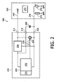
- FIG. 2 shows a circuit diagram of a current interface 200 according to a further embodiment of the invention. Apart from the diode 125, which is replaced by a voltage regulator 226, the components of the current interface 200 are identical to the components of the of the current interface 100 and will thus not be described once again in detail. The same holds for the control and evaluation unit 250, which is identical to the control and evaluation unit 150.
- the voltage regulator 226 comprises three terminals. A first terminal is connected to the first supply pin 211. A second terminal is connected to the signal generating and conditioning device 230. A third terminal is connected to the second supply pin 212.
- the voltage regulator 226 is used in order to stabilize the voltage over the signal generating and conditioning device 230. Therefore, unwanted voltage fluctuations may also be kept away from the signal generating and conditioning device 230 such that it is possible to provide for both a very sensitive signal generation and a very sensitive signal conditioning.
- the voltage regulator 226 has also the effect that current can only flow from the first supply pin 211 to the signal generating and conditioning device 230 and not in the opposite direction from the signal generating and conditioning device 230 to the first supply pin 211. Therefore, also the voltage regulator 226 has the effect that the blocking capacitor 228 is decoupled from the current source 220 such that the output signal of the current source 220 is not limited by a low-pass filter behavior.
- the decoupling of the blocking capacitor 228 from the current source 220 could also be realized if the voltage regulator 226 would be arranged within the low power supply line i.e. the conductor between the signal generating and conditioning device 230 and the second supply pin 212.
- the described sensor package 110, 210 may be used for any application, where information is transmitted digitally via a current interface.
- the described decoupling of the blocking capacitor 128, 228 from the current source 120, 220 is in particular suitable for magnetoresistive angular sensors, which one the one hand require a reliable blocking of voltage fluctuations from the signal generating and conditioning device 130, 230 and one the other hand allows for a signal output being not degenerated due to a low-pass behavior.
Landscapes
- Physics & Mathematics (AREA)
- General Physics & Mathematics (AREA)
- Arrangements For Transmission Of Measured Signals (AREA)
- Measurement Of Current Or Voltage (AREA)
- Structure Of Telephone Exchanges (AREA)
- Details Of Connecting Devices For Male And Female Coupling (AREA)
- Dc-Dc Converters (AREA)
- Measurement Of Length, Angles, Or The Like Using Electric Or Magnetic Means (AREA)
Claims (10)
- Eine Stromschnittstelle zum Bereitstellen eines Ausgabestromsignals, das mittels eines Sensoreingabesignals (135) gesteuert ist, wobei die Stromschnittstelle aufweist:einen ersten Zuführungsanschlussstift (111, 211), der geeignet ist, mit einer Versorgungsspannung (Vdd) verbunden zu werden,einen zweiten Zuführungsanschlussstift (112, 212), der geeignet ist, das Ausgabestromsignal bereitzustellen,eine Stromquelle (120, 220), die zwischen dem ersten Zuführungsanschlussstift (111, 211) und dem zweiten Zuführungsanschlussstift (112, 212) verbunden ist,dadurch gekennzeichnet, dass die Stromschnittstelle ferner einen zusätzlichen Anschlussstift (115, 215) aufweist, der geeignet ist, mittels eines Blockierkondensators (128, 228) mit einem der zwei Zuführungsanschlussstifte verbunden zu werden, undeine Entkopplungsvorrichtung (125, 226), die zwischen dem zusätzlichen Anschlussstift (115, 215) und dem anderen der zwei Zuführungsanschlussstifte verbunden ist.
- Die Stromschnittstelle nach Anspruch 1, die ferner aufweist:eine Signalaufbereitungseinheit (132, 232), die an die Stromquelle (120, 220) gekoppelt ist, um ein Steuersignal an die Stromquelle (120, 220) bereitzustellen.
- Die Stromschnittstelle nach Anspruch 2, wobei
die Signalaufbereitungseinheit (132, 232) geeignet ist, digitale Steuersignale (135, 235) an die Stromquelle (120, 220) bereitzustellen. - Die Stromschnittstelle nach Anspruch 2, wobei
die Signalaufbereitungseinheit (132, 232) mittels einer Versorgungsspannung angetrieben ist, die zwischen dem ersten Zuführungsanschlussstift (111, 211) und dem zusätzlichen Anschlussstift (115, 215) vorhanden ist. - Die Stromschnittstelle nach Anspruch 2, die ferner aufweist:ein Sensorelement (131, 231).
- Die Stromschnittstelle nach Anspruch 5, wobei
das Sensorelement (131, 231) integral mit der Signalaufbereitungseinheit (132, 232) ausgebildet ist. - Die Stromschnittstelle nach Anspruch 5, wobei
das Sensorelement (131, 231) ein Winkelsensor ist, insbesondere das Sensorelement ein magnetoresistiver Winkelsensor ist. - Die Stromschnittstelle nach Anspruch 2, wobei
der erste Zuführungsanschlussstift (111, 211), der zweite Zuführungsanschlussstift (112, 212) und der zusätzliche Anschlussstift (115, 215) die einzigen bereitgestellten Anschlussstifte sind. - Die Stromschnittstelle nach Anspruch 1, wobei
die Entkopplungsvorrichtung eine Diode (125) ist. - Die Stromschnittstelle nach Anspruch 1, wobei
die Entkopplungsvorrichtung ein Spannungsregler (226) ist.
Priority Applications (1)
| Application Number | Priority Date | Filing Date | Title |
|---|---|---|---|
| EP07735752A EP2020000B1 (de) | 2006-05-12 | 2007-05-03 | Stromschnittstelle mit einem an einen zusätzlichen pin angeschlossenen sperrkondensator |
Applications Claiming Priority (3)
| Application Number | Priority Date | Filing Date | Title |
|---|---|---|---|
| EP06113838 | 2006-05-12 | ||
| EP07735752A EP2020000B1 (de) | 2006-05-12 | 2007-05-03 | Stromschnittstelle mit einem an einen zusätzlichen pin angeschlossenen sperrkondensator |
| PCT/IB2007/051657 WO2007132389A1 (en) | 2006-05-12 | 2007-05-03 | Current interface with a blocking capacitor attached to an additional pin |
Publications (2)
| Publication Number | Publication Date |
|---|---|
| EP2020000A1 EP2020000A1 (de) | 2009-02-04 |
| EP2020000B1 true EP2020000B1 (de) | 2010-10-27 |
Family
ID=38528620
Family Applications (1)
| Application Number | Title | Priority Date | Filing Date |
|---|---|---|---|
| EP07735752A Not-in-force EP2020000B1 (de) | 2006-05-12 | 2007-05-03 | Stromschnittstelle mit einem an einen zusätzlichen pin angeschlossenen sperrkondensator |
Country Status (8)
| Country | Link |
|---|---|
| US (1) | US8143884B2 (de) |
| EP (1) | EP2020000B1 (de) |
| JP (1) | JP2009537036A (de) |
| KR (1) | KR20090009322A (de) |
| CN (1) | CN101443828B (de) |
| AT (1) | ATE486341T1 (de) |
| DE (1) | DE602007010126D1 (de) |
| WO (1) | WO2007132389A1 (de) |
Cited By (1)
| Publication number | Priority date | Publication date | Assignee | Title |
|---|---|---|---|---|
| DE102021133780A1 (de) | 2021-12-20 | 2023-06-22 | Dr. Ing. H.C. F. Porsche Aktiengesellschaft | Vorrichtung und Verfahren zum infrastrukturseitigen Verbinden und Trennen von Kontakten für eine Wechselstromverbindung zwischen einer Ladeinfrastruktur und einem zu ladenden Fahrzeug |
Families Citing this family (8)
| Publication number | Priority date | Publication date | Assignee | Title |
|---|---|---|---|---|
| DE102008000844A1 (de) * | 2008-03-27 | 2009-10-01 | Robert Bosch Gmbh | Sensorsteuerungsgerät für ein Fahrzeug und Verfahren zum Betrieb eines solchen Sensorsteuergeräts |
| US8656065B1 (en) * | 2013-01-29 | 2014-02-18 | Honeywell International Inc. | Method and apparatus for automatically selecting a plurality of modes for programmable interface circuit by coupling field devices to process controllers |
| US9618587B2 (en) | 2015-07-16 | 2017-04-11 | Ford Global Technologies, Llc | Two-wire hall-effect sensor |
| IT201600081667A1 (it) * | 2016-08-03 | 2018-02-03 | Roberto Lazzarotto | DISPOSITIVO CIRCUITALE CON FUNZIONALITà REED |
| IT201700068700A1 (it) * | 2017-06-20 | 2018-12-20 | Illinois Tool Works | Circuito elettronico di commutazione, procedimento e apparecchiatura corrispondenti |
| CN107576836A (zh) * | 2017-10-18 | 2018-01-12 | 叶有福 | 综合传感器 |
| CN108540122B (zh) * | 2018-05-02 | 2024-12-06 | 贵州华旭科技有限公司 | 一种通讯接口电路 |
| CN112327037B (zh) * | 2020-11-17 | 2024-05-14 | 深圳市海浦蒙特科技有限公司 | 一种霍尔电流传感器模块 |
Family Cites Families (32)
| Publication number | Priority date | Publication date | Assignee | Title |
|---|---|---|---|---|
| US2571915A (en) * | 1949-09-09 | 1951-10-16 | Westinghouse Electric Corp | Direct-current amplifier |
| US4169232A (en) * | 1977-08-29 | 1979-09-25 | The Bendix Corporation | Signal conditioning circuit for magnetic sensing means |
| DE3433777A1 (de) * | 1984-09-14 | 1986-03-27 | Robert Bosch Gmbh, 7000 Stuttgart | Impulsformer fuer induktive geber |
| DE3435867A1 (de) * | 1984-09-29 | 1986-04-10 | Bosch Gmbh Robert | Differentialsensor |
| DE3706306A1 (de) * | 1987-02-27 | 1988-09-08 | Standard Elektrik Lorenz Ag | Schaltung zur gewinnung eines temperaturunabhaengigen rechtecksignals aus einem messsignal |
| DE3708210A1 (de) * | 1987-03-13 | 1988-09-22 | Bosch Gmbh Robert | Schaltungsanordnung zur auswertung der signale eines induktiven messwertaufnehmers |
| DE3824557A1 (de) * | 1988-07-20 | 1990-01-25 | Thomson Brandt Gmbh | Schaltung zur umwandlung |
| US5455510A (en) * | 1994-03-11 | 1995-10-03 | Honeywell Inc. | Signal comparison circuit with temperature compensation |
| JPH10160748A (ja) * | 1996-12-03 | 1998-06-19 | Oki Electric Ind Co Ltd | 衝撃センサ |
| US6442502B1 (en) * | 1997-04-30 | 2002-08-27 | Continental Teves Ag & Co. Ohg | System for detecting rotating speed |
| JPH10332722A (ja) * | 1997-06-02 | 1998-12-18 | Matsushita Electric Ind Co Ltd | 回転速度検出装置 |
| DE19723645B4 (de) | 1997-06-05 | 2006-04-13 | Endress + Hauser Gmbh + Co. Kg | Anordnung zur Signalübertragung zwischen einer Geberstelle und einer Empfangsstelle |
| FR2781285A1 (fr) * | 1998-07-17 | 2000-01-21 | Koninkl Philips Electronics Nv | Dispositif de mesure automatique d'une resistance |
| EP0986039B1 (de) * | 1998-09-07 | 2008-10-29 | Endress + Hauser GmbH + Co. KG | Anordnung zur Stromversorgung einer Stromschleifesendestation |
| US6268721B1 (en) * | 1999-02-17 | 2001-07-31 | Delphi Technologies, Inc. | Low cost binary encoded crankshaft position sensor |
| US6204715B1 (en) * | 1999-02-26 | 2001-03-20 | General Motors Corporation | Signal amplifying circuit |
| US6310474B1 (en) * | 1999-03-31 | 2001-10-30 | Delphi Technologies, Inc. | Method and apparatus for detecting the direction of crankshaft rotation during a single tooth/slot transition |
| US6232770B1 (en) * | 1999-07-01 | 2001-05-15 | Delphi Technologies, Inc. | Low cost single magnetoresistor position and speed sensor |
| US6291989B1 (en) * | 1999-08-12 | 2001-09-18 | Delphi Technologies, Inc. | Differential magnetic position sensor with adaptive matching for detecting angular position of a toothed target wheel |
| AUPQ285899A0 (en) * | 1999-09-16 | 1999-10-07 | Britax Rainsfords Pty Ltd | Sensor memory electronic circuit |
| US6438364B1 (en) * | 2000-06-06 | 2002-08-20 | Philips Electronics North America Corporation | Radio frequency device with fast charging of an input capacitance |
| US6456063B1 (en) * | 2000-11-03 | 2002-09-24 | Delphi Technologies, Inc. | Self compensating control circuit for digital magnetic sensors |
| US6747425B2 (en) * | 2002-01-24 | 2004-06-08 | Asahi Kasei Microsystems Co. Ltd | System for sharing power and signal pins on a motor controller |
| US6697266B2 (en) * | 2002-03-04 | 2004-02-24 | University Of Hong Kong | Method and system for providing a DC voltage with low ripple by overlaying a plurality of AC signals |
| US6759843B2 (en) * | 2002-11-15 | 2004-07-06 | Honeywell International Inc. | Sensing methods and systems for hall and/or MR sensors |
| FR2855874B1 (fr) * | 2003-06-06 | 2005-08-05 | Siemens Vdo Automotive | Capteur de position angulaire absolue sur 360° d'un organe rotatif |
| US6727689B1 (en) * | 2003-07-24 | 2004-04-27 | Honeywell International Inc. | Magnetic-effect sensing apparatus with signal thresholding |
| JP2005134283A (ja) * | 2003-10-31 | 2005-05-26 | Aisin Seiki Co Ltd | 2線式の電流出力センサ及び該センサ用ic |
| US7528597B2 (en) * | 2004-03-08 | 2009-05-05 | Digisensors, Inc. | Induction sensor |
| GB0406278D0 (en) * | 2004-03-19 | 2004-04-21 | Inertia Switch Ltd | Fuel level sensor |
| US7474149B2 (en) * | 2005-03-25 | 2009-01-06 | Pulsewave Rf, Inc. | Radio frequency power amplifier and method using a controlled supply |
| US7888923B2 (en) * | 2009-03-27 | 2011-02-15 | Texas Instruments Incorporated | Dynamic phase manager for multi-phase switching regulators |
-
2007
- 2007-05-03 WO PCT/IB2007/051657 patent/WO2007132389A1/en not_active Ceased
- 2007-05-03 JP JP2009508620A patent/JP2009537036A/ja not_active Withdrawn
- 2007-05-03 DE DE602007010126T patent/DE602007010126D1/de active Active
- 2007-05-03 KR KR1020087030198A patent/KR20090009322A/ko not_active Abandoned
- 2007-05-03 AT AT07735752T patent/ATE486341T1/de not_active IP Right Cessation
- 2007-05-03 US US12/300,375 patent/US8143884B2/en not_active Expired - Fee Related
- 2007-05-03 EP EP07735752A patent/EP2020000B1/de not_active Not-in-force
- 2007-05-03 CN CN2007800168265A patent/CN101443828B/zh not_active Expired - Fee Related
Cited By (1)
| Publication number | Priority date | Publication date | Assignee | Title |
|---|---|---|---|---|
| DE102021133780A1 (de) | 2021-12-20 | 2023-06-22 | Dr. Ing. H.C. F. Porsche Aktiengesellschaft | Vorrichtung und Verfahren zum infrastrukturseitigen Verbinden und Trennen von Kontakten für eine Wechselstromverbindung zwischen einer Ladeinfrastruktur und einem zu ladenden Fahrzeug |
Also Published As
| Publication number | Publication date |
|---|---|
| EP2020000A1 (de) | 2009-02-04 |
| WO2007132389A1 (en) | 2007-11-22 |
| ATE486341T1 (de) | 2010-11-15 |
| US20090262860A1 (en) | 2009-10-22 |
| DE602007010126D1 (de) | 2010-12-09 |
| JP2009537036A (ja) | 2009-10-22 |
| CN101443828B (zh) | 2012-07-04 |
| US8143884B2 (en) | 2012-03-27 |
| CN101443828A (zh) | 2009-05-27 |
| KR20090009322A (ko) | 2009-01-22 |
Similar Documents
| Publication | Publication Date | Title |
|---|---|---|
| EP2020000B1 (de) | Stromschnittstelle mit einem an einen zusätzlichen pin angeschlossenen sperrkondensator | |
| US6054780A (en) | Magnetically coupled signal isolator using a Faraday shielded MR or GMR receiving element | |
| US9660303B2 (en) | Battery monitoring system | |
| US6750808B2 (en) | Process instrument with split intrinsic safety barrier | |
| EP3519777B1 (de) | Verschiebungssensor zur kontaktlosen messung einer relativen position, verfahren zur herstellung einer magnetfeldsensoranordnung und magnetfeldsensor | |
| EP1403832B2 (de) | Intrinsisch sichere explosionssichere sensorschaltung | |
| EP1518128A2 (de) | Zellenpuffer mit eingebautem test | |
| EP1424562B1 (de) | Vorrichtung und verfahren zur messung der sensorkapazität | |
| EP1329698A2 (de) | Pegelsensor mit mehreren Eingangskanälen | |
| US4950998A (en) | Continuous condition sensing system | |
| US8692541B2 (en) | Position sensing head with redundancy | |
| EP0764292B1 (de) | Wandler mit elektrischer schaltung zum verhindern der entladung von gespeicherter energie | |
| WO1986000144A1 (en) | Digital accelerometer | |
| US5278513A (en) | Continuous condition sensing system | |
| US11271386B2 (en) | Electronic temperature switch | |
| US20250306558A1 (en) | Intrinsically safe automation field device | |
| EP4457489A1 (de) | Anpassung von prozessvariablen sendern mit hermetisch abgedichteter emi-schutzelektronik | |
| RU2646311C1 (ru) | Система передачи сигналов от датчиков с аналоговым выходом по двухпроводной линии связи | |
| CN223581209U (zh) | 一种温度采集电路及温度检测系统 | |
| US11933639B2 (en) | Sensing system comprising a chain of sensors | |
| Leilei et al. | Research and development for landing gear test interface unit for one type aircraft | |
| JP4223632B2 (ja) | 電流検出回路 | |
| US6677686B1 (en) | Redundant power supply system with improved reference voltage sampling at low loads | |
| ADVFC32S | ADVFC32–SPECIFICATIONS (typical@ 25 C with VS= 15 V unless otherwise noted.) | |
| WO2023150442A1 (en) | Customization of process variable transmitters with hermetically sealed emi protection electronics |
Legal Events
| Date | Code | Title | Description |
|---|---|---|---|
| PUAI | Public reference made under article 153(3) epc to a published international application that has entered the european phase |
Free format text: ORIGINAL CODE: 0009012 |
|
| 17P | Request for examination filed |
Effective date: 20081212 |
|
| AK | Designated contracting states |
Kind code of ref document: A1 Designated state(s): AT BE BG CH CY CZ DE DK EE ES FI FR GB GR HU IE IS IT LI LT LU LV MC MT NL PL PT RO SE SI SK TR |
|
| AX | Request for extension of the european patent |
Extension state: AL BA HR MK RS |
|
| GRAP | Despatch of communication of intention to grant a patent |
Free format text: ORIGINAL CODE: EPIDOSNIGR1 |
|
| GRAS | Grant fee paid |
Free format text: ORIGINAL CODE: EPIDOSNIGR3 |
|
| GRAA | (expected) grant |
Free format text: ORIGINAL CODE: 0009210 |
|
| AK | Designated contracting states |
Kind code of ref document: B1 Designated state(s): AT BE BG CH CY CZ DE DK EE ES FI FR GB GR HU IE IS IT LI LT LU LV MC MT NL PL PT RO SE SI SK TR |
|
| REG | Reference to a national code |
Ref country code: GB Ref legal event code: FG4D |
|
| REG | Reference to a national code |
Ref country code: CH Ref legal event code: EP |
|
| REG | Reference to a national code |
Ref country code: IE Ref legal event code: FG4D |
|
| REF | Corresponds to: |
Ref document number: 602007010126 Country of ref document: DE Date of ref document: 20101209 Kind code of ref document: P |
|
| REG | Reference to a national code |
Ref country code: NL Ref legal event code: VDEP Effective date: 20101027 |
|
| LTIE | Lt: invalidation of european patent or patent extension |
Effective date: 20101027 |
|
| PG25 | Lapsed in a contracting state [announced via postgrant information from national office to epo] |
Ref country code: LT Free format text: LAPSE BECAUSE OF FAILURE TO SUBMIT A TRANSLATION OF THE DESCRIPTION OR TO PAY THE FEE WITHIN THE PRESCRIBED TIME-LIMIT Effective date: 20101027 |
|
| PG25 | Lapsed in a contracting state [announced via postgrant information from national office to epo] |
Ref country code: BG Free format text: LAPSE BECAUSE OF FAILURE TO SUBMIT A TRANSLATION OF THE DESCRIPTION OR TO PAY THE FEE WITHIN THE PRESCRIBED TIME-LIMIT Effective date: 20110127 Ref country code: SE Free format text: LAPSE BECAUSE OF FAILURE TO SUBMIT A TRANSLATION OF THE DESCRIPTION OR TO PAY THE FEE WITHIN THE PRESCRIBED TIME-LIMIT Effective date: 20101027 Ref country code: FI Free format text: LAPSE BECAUSE OF FAILURE TO SUBMIT A TRANSLATION OF THE DESCRIPTION OR TO PAY THE FEE WITHIN THE PRESCRIBED TIME-LIMIT Effective date: 20101027 Ref country code: AT Free format text: LAPSE BECAUSE OF FAILURE TO SUBMIT A TRANSLATION OF THE DESCRIPTION OR TO PAY THE FEE WITHIN THE PRESCRIBED TIME-LIMIT Effective date: 20101027 Ref country code: NL Free format text: LAPSE BECAUSE OF FAILURE TO SUBMIT A TRANSLATION OF THE DESCRIPTION OR TO PAY THE FEE WITHIN THE PRESCRIBED TIME-LIMIT Effective date: 20101027 Ref country code: SI Free format text: LAPSE BECAUSE OF FAILURE TO SUBMIT A TRANSLATION OF THE DESCRIPTION OR TO PAY THE FEE WITHIN THE PRESCRIBED TIME-LIMIT Effective date: 20101027 Ref country code: LV Free format text: LAPSE BECAUSE OF FAILURE TO SUBMIT A TRANSLATION OF THE DESCRIPTION OR TO PAY THE FEE WITHIN THE PRESCRIBED TIME-LIMIT Effective date: 20101027 Ref country code: PT Free format text: LAPSE BECAUSE OF FAILURE TO SUBMIT A TRANSLATION OF THE DESCRIPTION OR TO PAY THE FEE WITHIN THE PRESCRIBED TIME-LIMIT Effective date: 20110228 Ref country code: IS Free format text: LAPSE BECAUSE OF FAILURE TO SUBMIT A TRANSLATION OF THE DESCRIPTION OR TO PAY THE FEE WITHIN THE PRESCRIBED TIME-LIMIT Effective date: 20110227 |
|
| PG25 | Lapsed in a contracting state [announced via postgrant information from national office to epo] |
Ref country code: GR Free format text: LAPSE BECAUSE OF FAILURE TO SUBMIT A TRANSLATION OF THE DESCRIPTION OR TO PAY THE FEE WITHIN THE PRESCRIBED TIME-LIMIT Effective date: 20110128 Ref country code: BE Free format text: LAPSE BECAUSE OF FAILURE TO SUBMIT A TRANSLATION OF THE DESCRIPTION OR TO PAY THE FEE WITHIN THE PRESCRIBED TIME-LIMIT Effective date: 20101027 |
|
| PG25 | Lapsed in a contracting state [announced via postgrant information from national office to epo] |
Ref country code: EE Free format text: LAPSE BECAUSE OF FAILURE TO SUBMIT A TRANSLATION OF THE DESCRIPTION OR TO PAY THE FEE WITHIN THE PRESCRIBED TIME-LIMIT Effective date: 20101027 Ref country code: CZ Free format text: LAPSE BECAUSE OF FAILURE TO SUBMIT A TRANSLATION OF THE DESCRIPTION OR TO PAY THE FEE WITHIN THE PRESCRIBED TIME-LIMIT Effective date: 20101027 Ref country code: ES Free format text: LAPSE BECAUSE OF FAILURE TO SUBMIT A TRANSLATION OF THE DESCRIPTION OR TO PAY THE FEE WITHIN THE PRESCRIBED TIME-LIMIT Effective date: 20110207 |
|
| PG25 | Lapsed in a contracting state [announced via postgrant information from national office to epo] |
Ref country code: PL Free format text: LAPSE BECAUSE OF FAILURE TO SUBMIT A TRANSLATION OF THE DESCRIPTION OR TO PAY THE FEE WITHIN THE PRESCRIBED TIME-LIMIT Effective date: 20101027 Ref country code: SK Free format text: LAPSE BECAUSE OF FAILURE TO SUBMIT A TRANSLATION OF THE DESCRIPTION OR TO PAY THE FEE WITHIN THE PRESCRIBED TIME-LIMIT Effective date: 20101027 Ref country code: DK Free format text: LAPSE BECAUSE OF FAILURE TO SUBMIT A TRANSLATION OF THE DESCRIPTION OR TO PAY THE FEE WITHIN THE PRESCRIBED TIME-LIMIT Effective date: 20101027 Ref country code: RO Free format text: LAPSE BECAUSE OF FAILURE TO SUBMIT A TRANSLATION OF THE DESCRIPTION OR TO PAY THE FEE WITHIN THE PRESCRIBED TIME-LIMIT Effective date: 20101027 |
|
| PLBE | No opposition filed within time limit |
Free format text: ORIGINAL CODE: 0009261 |
|
| STAA | Information on the status of an ep patent application or granted ep patent |
Free format text: STATUS: NO OPPOSITION FILED WITHIN TIME LIMIT |
|
| 26N | No opposition filed |
Effective date: 20110728 |
|
| REG | Reference to a national code |
Ref country code: DE Ref legal event code: R097 Ref document number: 602007010126 Country of ref document: DE Effective date: 20110728 |
|
| PG25 | Lapsed in a contracting state [announced via postgrant information from national office to epo] |
Ref country code: IT Free format text: LAPSE BECAUSE OF FAILURE TO SUBMIT A TRANSLATION OF THE DESCRIPTION OR TO PAY THE FEE WITHIN THE PRESCRIBED TIME-LIMIT Effective date: 20101027 Ref country code: MT Free format text: LAPSE BECAUSE OF FAILURE TO SUBMIT A TRANSLATION OF THE DESCRIPTION OR TO PAY THE FEE WITHIN THE PRESCRIBED TIME-LIMIT Effective date: 20101027 Ref country code: MC Free format text: LAPSE BECAUSE OF NON-PAYMENT OF DUE FEES Effective date: 20110531 |
|
| REG | Reference to a national code |
Ref country code: CH Ref legal event code: PL |
|
| PG25 | Lapsed in a contracting state [announced via postgrant information from national office to epo] |
Ref country code: CH Free format text: LAPSE BECAUSE OF NON-PAYMENT OF DUE FEES Effective date: 20110531 Ref country code: LI Free format text: LAPSE BECAUSE OF NON-PAYMENT OF DUE FEES Effective date: 20110531 |
|
| REG | Reference to a national code |
Ref country code: IE Ref legal event code: MM4A |
|
| PG25 | Lapsed in a contracting state [announced via postgrant information from national office to epo] |
Ref country code: IE Free format text: LAPSE BECAUSE OF NON-PAYMENT OF DUE FEES Effective date: 20110503 |
|
| PG25 | Lapsed in a contracting state [announced via postgrant information from national office to epo] |
Ref country code: LU Free format text: LAPSE BECAUSE OF NON-PAYMENT OF DUE FEES Effective date: 20110503 Ref country code: CY Free format text: LAPSE BECAUSE OF FAILURE TO SUBMIT A TRANSLATION OF THE DESCRIPTION OR TO PAY THE FEE WITHIN THE PRESCRIBED TIME-LIMIT Effective date: 20101027 |
|
| PG25 | Lapsed in a contracting state [announced via postgrant information from national office to epo] |
Ref country code: TR Free format text: LAPSE BECAUSE OF FAILURE TO SUBMIT A TRANSLATION OF THE DESCRIPTION OR TO PAY THE FEE WITHIN THE PRESCRIBED TIME-LIMIT Effective date: 20101027 |
|
| PG25 | Lapsed in a contracting state [announced via postgrant information from national office to epo] |
Ref country code: HU Free format text: LAPSE BECAUSE OF FAILURE TO SUBMIT A TRANSLATION OF THE DESCRIPTION OR TO PAY THE FEE WITHIN THE PRESCRIBED TIME-LIMIT Effective date: 20101027 |
|
| REG | Reference to a national code |
Ref country code: FR Ref legal event code: PLFP Year of fee payment: 9 |
|
| REG | Reference to a national code |
Ref country code: FR Ref legal event code: PLFP Year of fee payment: 10 |
|
| REG | Reference to a national code |
Ref country code: FR Ref legal event code: PLFP Year of fee payment: 11 |
|
| REG | Reference to a national code |
Ref country code: FR Ref legal event code: PLFP Year of fee payment: 12 |
|
| PGFP | Annual fee paid to national office [announced via postgrant information from national office to epo] |
Ref country code: DE Payment date: 20190418 Year of fee payment: 13 |
|
| PGFP | Annual fee paid to national office [announced via postgrant information from national office to epo] |
Ref country code: FR Payment date: 20190418 Year of fee payment: 13 |
|
| PGFP | Annual fee paid to national office [announced via postgrant information from national office to epo] |
Ref country code: GB Payment date: 20190423 Year of fee payment: 13 |
|
| REG | Reference to a national code |
Ref country code: DE Ref legal event code: R119 Ref document number: 602007010126 Country of ref document: DE |
|
| GBPC | Gb: european patent ceased through non-payment of renewal fee |
Effective date: 20200503 |
|
| PG25 | Lapsed in a contracting state [announced via postgrant information from national office to epo] |
Ref country code: FR Free format text: LAPSE BECAUSE OF NON-PAYMENT OF DUE FEES Effective date: 20200531 Ref country code: GB Free format text: LAPSE BECAUSE OF NON-PAYMENT OF DUE FEES Effective date: 20200503 |
|
| PG25 | Lapsed in a contracting state [announced via postgrant information from national office to epo] |
Ref country code: DE Free format text: LAPSE BECAUSE OF NON-PAYMENT OF DUE FEES Effective date: 20201201 |