EP2020029B1 - Verbesserte cmos-dioden mit doppelgate-leitern und verfahren zu ihrer herstellung - Google Patents
Verbesserte cmos-dioden mit doppelgate-leitern und verfahren zu ihrer herstellung Download PDFInfo
- Publication number
- EP2020029B1 EP2020029B1 EP07761243A EP07761243A EP2020029B1 EP 2020029 B1 EP2020029 B1 EP 2020029B1 EP 07761243 A EP07761243 A EP 07761243A EP 07761243 A EP07761243 A EP 07761243A EP 2020029 B1 EP2020029 B1 EP 2020029B1
- Authority
- EP
- European Patent Office
- Prior art keywords
- region
- gate
- doped
- dielectric
- semiconductor substrate
- Prior art date
- Legal status (The legal status is an assumption and is not a legal conclusion. Google has not performed a legal analysis and makes no representation as to the accuracy of the status listed.)
- Not-in-force
Links
Images


Classifications
-
- H—ELECTRICITY
- H10—SEMICONDUCTOR DEVICES; ELECTRIC SOLID-STATE DEVICES NOT OTHERWISE PROVIDED FOR
- H10D—INORGANIC ELECTRIC SEMICONDUCTOR DEVICES
- H10D12/00—Bipolar devices controlled by the field effect, e.g. insulated-gate bipolar transistors [IGBT]
- H10D12/211—Gated diodes
-
- H—ELECTRICITY
- H10—SEMICONDUCTOR DEVICES; ELECTRIC SOLID-STATE DEVICES NOT OTHERWISE PROVIDED FOR
- H10D—INORGANIC ELECTRIC SEMICONDUCTOR DEVICES
- H10D12/00—Bipolar devices controlled by the field effect, e.g. insulated-gate bipolar transistors [IGBT]
- H10D12/01—Manufacture or treatment
- H10D12/021—Manufacture or treatment of gated diodes, e.g. field-controlled diodes [FCD]
Definitions
- the present invention relates to improved complementary metal-oxide-semiconductor (CMOS) diode structures. More specifically, the present invention relates to CMOS diodes having dual gate conductors, which function to reduce the P+/N+ variation and the ideality variation of the CMOS diodes.
- CMOS complementary metal-oxide-semiconductor
- FIG. 1 shows a conventional CMOS diode formed in a semiconductor substrate 110.
- the semiconductor substrate 110 comprises a first region 112 that has n-type conductivity and a second region 114 that has p-type conductivity.
- the first and second regions 112 and 114 jointly define a third region 113 located therebetween in the semiconductor substrate 110, which has either n-type or p-type conductivity, but at a significantly lower dopant concentration in comparison with the first or second regions 112 or 114.
- the first and second regions 112 and 114 may also comprise surface silicide layers 112A and 114A, as shown in FIG. 1 .
- the CMOS diode is typically defined by a single gate conductor, which is located over a gate dielectric layer 120 on top of the semiconductor substrate 110 and which includes a first portion 122 of n-type conductivity and a second portion 124 of p-type conductivity, as shown in FIG. 1 .
- the first portion 122 of the gate conductor is located adjacent to the first region 112, and the second portion 124 is located adjacent to the second region 114.
- the first and second portions 122 and 124 of the gate conductor are in direct contact with each other and are shorted by a common surface silicide layer 123.
- One or more optional sidewall spacers 126 may optionally be provided along sidewalls of the gate conductor to isolate the gate conductor from the first and second doped regions 112 and 114. Further, one or more dielectric cap layer 130 can be provided over the entire structure, including the gate conductor as well as the semiconductor substrate 110.
- a carrier accumulation region 116 is formed in the lightly n-doped third region 113 of the semiconductor substrate 110 and immediately underneath the p-doped second portion 124 of the gate conductor, due to the work function difference between the n-doped and p-doped regions. Further, a depletion region 118 is formed under the carrier accumulation region 116 at the diode interface between the lightly n-doped third region 113 and the p-doped second region 114, as shown in FIG. 1 .
- the widths of the accumulation region 116 and the depletion region 118 are positively correlated with that of the p-doped second portion 124 of the gate conductor.
- doping of the first and second portions 122 and 124 of the single gate conductor is typically achieved by masked dopant implantation, which, due to limitations of the lithographic tools used, can result in significant overlay mis-alignment and critical dimension (CD) variations. Therefore, the width of the resulting p-doped second portion 124 of the gate conductor may vary significantly. Consequently, the widths of the accumulation region 116 and the depletion region 118 may vary significantly, which in turn leads to deleterious electric field variation at the diode interface.
- the width of the accumulation region 116 and its interaction with the underlying depletion region 118 directly impact the diode ideality, because the diode ideality is adversely affected by electron/hole recombination occurred in the depletion region 118, and because the accumulation region 116 provides an source of electrons in addition to the lightly n-doped third region 113, which increases the likelihood of electron/hole recombination in the depletion region 118. Consequently, the width variations generated by the masked dopant implantation lead to significantly large ideality variations ( ⁇ 4%) in the CMOS diodes currently available for the 90 nm node circuits, which is far beyond the desired variation limit.
- US Patents 6,861,680 and 6,232,163 disclose a dual gated diode with p doed and n doped gates respectively adjacent corresponding p and n doped regionas, the gates being in contact.
- US Patent 5,468,669 discloses a CMOS device with n doped and p doped gates respectively. the gates are physically and electrically connected by a low resistance layer.
- the present invention provides improved CMOS diodes with dual gate conductors, one of which is doped with n-type dopant species and the other is doped with p-type dopant species.
- the widths of the P+/N+ doped regions in such dual gate conductors are determined by a gate patterning process, instead of the error-prone masked dopant implantation process, and therefore have significantly reduced variations. Consequently, the ideality factor variations in such improved CMOS diodes are advantageously reduced.
- the present invention provides a semiconductor device comprising: a semiconductor substrate comprising a first doped region of n-type conductivity and a second doped region of p-type conductivity with a third doped region located therebetween, wherein the third doped region has either n-type or p-type conductivity with a dopant concentration lower than that of the first or second region; a gate dielectric layer located over the semiconductor substrate; a first gate conductor of n-type conductivity, which is located on the dielectric layer adjacent to the first doped region in the semiconductor substrate; and a second gate conductor of p-type conductivity, which is located on the dielectric layer adjacent to the second doped region in the semiconductor substrate and which is spaced apart and isolated from the first gate conductor by a dielectric isolation structure therebetween, wherein the first, second, and third doped regions and the first and second gate conductors are arranged and constructed to form an accumulation region and an underlying depletion region between the third doped region and the second or the first doped region.
- the dielectric isolation structure comprises a dielectric material selected from the group consisting of oxides, nitrides, and oxynitrides.
- the dielectric isolation structure comprises silicon nitride.
- the dielectric isolation structure comprises silicon oxide.
- the first and second doped regions and the first and second gate conductors may each comprise a surface silicide layer.
- one or more dielectric spacers may be provided along sidewalls of the first and second gate conductors.
- the dielectric spacers comprise one or more oxide spacers and/or nitride spacers.
- a dielectric cap layer can be provided over the first and second gate conductors and the semiconductor substrate for capping the semiconductor device.
- the present invention relates to a semiconductor device comprising: a semiconductor substrate comprising a first doped region of n-type conductivity and a second doped region of p-type conductivity with a third doped region located therebetween, wherein the third doped region has n-type conductivity with a dopant concentration lower than that of the first region; a gate dielectric layer located over the semiconductor substrate; a first gate conductor of n-type conductivity, which is located on the dielectric layer adjacent to the first doped region in the semiconductor substrate; and a second gate conductor of p-type conductivity, which is located on the dielectric layer adjacent to the second doped region in the semiconductor substrate and which is spaced apart and isolated from the first gate conductor by a dielectric isolation structure therebetween, wherein the first, second, and third doped regions and the first and second gate conductors are arranged and constructed to form an accumulation region and an underlying depletion region between the third doped region and the second doped region.
- the present invention relates to a semiconductor device comprising: a semiconductor substrate comprising a first doped region of n-type conductivity and a second doped region of p-type conductivity with a third doped region located therebetween, wherein the third doped region has p-type conductivity with a dopant concentration lower than that of the second region; a gate dielectric layer located over the semiconductor substrate; a first gate conductor of n-type conductivity, which is located on the dielectric layer adjacent to the first doped region in the semiconductor substrate; and a second gate conductor of p-type conductivity, which is located on the dielectric layer adjacent to the second doped region in the semiconductor substrate and which is spaced apart and isolated from the first gate conductor by a dielectric isolation structure therebetween, wherein the first, second, and third doped regions and the first and second gate conductors are arranged and constructed to form an accumulation region and an underlying between the third doped region and the first doped region.
- the present invention relates to a method for forming a semiconductor device, comprising: forming a gate dielectric layer over a semiconductor substrate that has a well region of either n-type or p-type conductivity located therein; forming first and second gate conductors over the gate dielectric layer, wherein the first and second gate conductors are spaced apart from each other; forming a dielectric isolation structure between the first and second gate conductors; selectively doping the first gate conductor and a first region in the well-region of the semiconductor substrate with an n-type dopant species; and selectively doping the second gate conductor and a second region in the well-region of the semiconductor substrate with a p-type dopant species, said second region being spaced apart from the first region and thereby defining a third region therebetween in the well region, wherein the first, second and third doped regions and the first and second gate conductors are arranged and constructed to form an accumulation region and an underlying depletion region between the third region and
- the well region of the semiconductor substrate has n-type conductivity.
- the accumulation region and the underlying depletion region are correspondingly formed between the third region and the second region, and the accumulation region has a width that is positively correlated with that of the second gate conductor.
- the well region of the semiconductor substrate has p-type conductivity.
- the accumulation region and the underlying depletion region are then formed between the third region and the first region, and the accumulation region has a width that is positively correlated with that of the first gate conductor.
- the dielectric isolation structure that isolates the first and second gate conductors can be formed by any suitable method. Preferably, but not necessarily, it is formed by depositing a blanket dielectric layer over both the first and second gate conductors, followed by patterning at least a portion of the blanket dielectric layer to form the dielectric isolation structure located between the first and second gate conductors. More preferably, additional portions of the blanket dielectric layers are patterned into one or more dielectric spacers along sidewalls of the first and second gate conductors.
- the present invention provides improved CMOS diodes with dual gate conductors.
- the CMOS diodes of the present invention each contains a first gate conductor of n-type conductivity and a second gate conductor of p-type conductivity, while the first and second gate conductors are isolated from each other by a dielectric isolation structure located therebetween.
- FIG. 2 shows a cross-sectional view of an exemplary CMOS diode, according to one embodiment of the present invention.
- the exemplary CMOS diode is formed in a semiconductor substrate 10, which may comprise any suitable semiconductor material, which includes, but is not limited to: Si, SiC, SiGe, SiGeC, Ge alloys, GaAs, InAs, InP, as well as other III-V or II-VI compound semiconductors, either in their single crystalline or polycrystalline form.
- the semiconductor substrate 10 may also comprise an organic semiconductor or a layered semiconductor such as Si/SiGe, a silicon-on-insulator (SOI) or a SiGe-on-insulator (SGOI).
- the semiconductor substrate 10 is composed of a Si-containing semiconductor material, i.e., a semiconductor material that includes silicon. More preferably, the semiconductor substrate 10 consists essentially of bulk single crystal silicon.
- the semiconductor substrate 10 may comprise one or more buried insulator layers (not shown) therein and thereby form a semiconductor-on-insulator (SOI) configuration.
- the semiconductor substrate 10 is preferably doped with either an n-type or a p-type dopant species at a relatively low dopant concentration (e.g., from about 1 ⁇ 10 14 /cm 2 to about 1 ⁇ 10 15 /cm 2 ).
- the semiconductor substrate 10 may comprise a well region (not shown) that is doped with either an n-type or a p-type dopant species at a relatively low dopant concentration.
- a first doped region 12 having a relatively high concentration (e.g., from about 1 ⁇ 10 15 /cm 2 to about 1 ⁇ 10 16 /cm 2 ) of n-type dopant species (i.e., the n + -doped region) and a second doped region 14 having a relatively high concentration of p-type dopant species (i.e., the p + -doped region) are further provided in the semiconductor substrate 10 in a spaced-apart relationship from each other.
- a third doped region 13 with n-type (as shown in FIG. 2 ) or p-type (not shown) dopant species at a relatively low dopant concentration (i.e., the n- or p-doped region) is defined by the spaced-apart first and second doped regions 12 and 14.
- the gate structure of the present invention comprises: (1) a gate dielectric layer 20, which is formed directly over the semiconductor substrate 10, (2) a first gate conductor 22, which is doped with a n-type dopant species at a relatively high dopant concentration and which is located over the gate dielectric layer 20 adjacent to the first doped region 12, and (3) a second gate conductor 24, which is doped with a p-type dopant species at a relatively high dopant concentration and which is also located over the gate dielectric layer 20 but adjacent to the second doped region 14.
- the first and second gate conductors 22 and 24 are spaced apart from each other by a dielectric isolation structure 23 that is located therebetween.
- the gate structure of the present invention may comprise one or more optional dielectric spacers 26 along sidewalls of the first and second gate conductors 22 and 24.
- the third doped region 13 contains n-type dopant species.
- an N/P diode interface is formed between the third doped region 13 (i.e., the n-doped region) and the second doped region 14 (i.e., the p + -doped region).
- a carrier accumulation region 16 is generated immediately underneath the second gate conductor 24, due to the work function difference between the n-doped and p-doped regions.
- carrier depletion region 18 underneath the carried accumulation region 16 along the N/P diode interface, which is located between the third doped region 13 (i.e., the n-doped region) and the second doped region 14 (i.e., the p + -doped region).
- the width of the accumulation region 16 is determined by, and positively correlated with, the width of the second gate conductor 24. Because the second gate conductor 24 is structurally isolated from the first gate conductor 22 by the dielectric isolation structure 23, the width of the second gate conductor 24 is determined solely by the gate patterning process (as described in more detail hereinafter) and is no longer affected by any potential overlay misalignment occurred during the masked dopant implantation process. Therefore, width variation of the second gate conductor 24 is significantly reduced, which leads to reduction in the width variation of the carrier accumulation region 16 and its interaction with the underlying depletion region 18 and thereby reduces diode ideality variation.
- the third doped region 13 may contain p-type dopant species (not shown).
- an N/P diode interface is formed between the first doped region 12 (i.e., the n + -doped region) and the third doped region 13 (i.e., the p-doped region).
- a carrier accumulation region (not shown) is generated immediately underneath the first gate conductor 22, due to the work function difference between the n-doped and p-doped regions.
- the width of the carrier accumulation region is then determined by, and positively correlated with, the width of the first gate conductor 22.
- the width of the first gate conductor 22 is determined solely by the gate patterning process (as described in more detail hereinafter) and is no longer affected by the potential overlay misalignment occurred during the masked dopant implantation process. Therefore, width variation of the first gate conductor 22 is significantly reduced, which leads to reduction in the width variation of the carrier accumulation region (not shown) and its interaction with the underlying depletion region (not shown) and thereby reduce diode ideality variation.
- the CMOS diode structure as shown in FIG. 2 further comprises optional silicide layers 12A, 14A, 22A and 24 A respectively located over the surfaces of the first doped region 12, the second doped region 14, the first gate conductor 22 and the second gate conductor 24.
- a dielectric cap layer 30 can also be provided over the entire CMOS diode structure to isolate such a CMOS diode from back-end-of-line (BEOL) interconnects.
- FIG. 2 illustratively demonstrates an exemplary CMOS diode device structure according to a specific embodiment of the present invention, it is clear that a person ordinarily skilled in the art can readily modify the exemplary device structure for adaptation to specific application requirements, consistent with the above descriptions.
- CMOS diode structure of the present invention can be readily formed by a fabrication process that is compatible with and can be readily integrated into the conventional CMOS process, with few or no additional processing steps. Specifically, exemplary processing steps for fabricating the CMOS diode structure of FIG. 2 are illustrated hereinafter by FIGS. 3-9 .
- the gate dielectric layer 20 may be comprised of any suitable dielectric material, including, but not limited to: oxides, nitrides, oxynitrides and/or silicates (including metal silicates and nitrided metal silicates). In one embodiment, it is preferred that the gate dielectric layer 20 is comprised of an oxide such as, for example, SiO 2 , HfO 2 , ZrO 2 , Al 2 O 3 , TiO 2 , La 2 O 3 , SrTiO 3 , LaAlO 3 , and mixtures thereof.
- oxides such as, for example, SiO 2 , HfO 2 , ZrO 2 , Al 2 O 3 , TiO 2 , La 2 O 3 , SrTiO 3 , LaAlO 3 , and mixtures thereof.
- the physical thickness of the gate dielectric layer 20 may vary, but typically, the gate dielectric layer 24 has a thickness from about 0.5 to about 10 nm, with a thickness from about 1 to about 5 nm being more typical.
- the gate dielectric layer 20 can be formed by a thermal growing process such as, for example, oxidation, nitridation or oxynitridation.
- the gate dielectric layer 20 can be formed by a deposition process such as, for example, chemical vapor deposition (CVD), plasma-assisted CVD, atomic layer deposition (ALD), evaporation, reactive sputtering, chemical solution deposition and other like deposition processes.
- the gate dielectric layer 20 may also be formed utilizing any combination of the above processes.
- two or more spaced-apart gate conductors 22 and 24 are formed over the gate dielectric layer 20, by first depositing a blanket gate conductor layer (not shown) over the gate dielectric layer 20, followed by patterning the blanket gate conductor layer into the spaced-apart gate conductors 22 and 24 by conventional lithography and etching.
- the lithography step preferably inverse gate level (PC) lithography, includes applying a photoresist (not shown) to the upper surface of the blanket gate conductor layer (not shown), exposing the photoresist to a desired pattern of radiation and developing the exposed photoresist utilizing a conventional resist developer.
- PC inverse gate level
- the pattern in the photoresist is then transferred to the gate conductor layer (not shown) utilizing one or more dry etching steps to form etch openings.
- Suitable dry etching processes that can be used in the present invention in patterning the blanket gate conductor layer (not shown) include, but are not limited to: reactive ion etching (RIE), ion beam etching, plasma etching or laser ablation.
- the gate conductor layer comprises polycrystalline silicon (poly-Si), and etching is carried out by a poly-Si RIE step that stops on the gate dielectric layer 20.
- the patterned photoresist is then removed by resist stripping after etching has been completed.
- An optional oxide liner 25 can be formed over the first and second gate conductors 22 and 24 by a conventional re-oxidation process or low temperature oxidation (LTO) process, as shown in FIG. 5 .
- LTO low temperature oxidation
- a blanket dielectric layer 27 is deposited over the entire structure to cover both the first and second gate conductor 22 and 24, as shown in FIG. 6 .
- the blanket dielectric layer 27 may comprise any suitable dielectric material, including, but not limited to: oxides, nitrides, oxynitrides, or any combination thereof.
- the blanket dielectric layer 27 comprises silicon nitride.
- the blanket dielectric layer 27 can be deposited utilizing a deposition process such as, for example, physical vapor deposition or chemical vapor deposition.
- the blanket dielectric layer 27 has a thickness ranging from about 50 nm to about 150 nm, and more preferably from about 80 nm to about 120 nm.
- the blanket dielectric layer 27 is then patterned by conventional lithography and etching (similar to those described hereinabove) to form a dielectric isolation structure 23, which is preferably a silicon nitride isolation structure, located between the first and second gate conductors 22 and 24, as shown in FIG. 7 .
- the blanket dielectric layer 27 is also patterned to form the optional silicon nitride spacers 26 along sidewalls of the first and second gate conductors 22 and 24.
- a first masked dopant implantation step is then carried out to selectively dope the first gate conductor 22 and an adjacent region 12 of the semiconductor substrate 10, thereby forming the n + -doped first gate conductor 22 and the n + -doped first region 12 in the semiconductor substrate 10, as shown in FIG. 8 .
- a second masked dopant implantation step is carried out to selectively dope the second gate conductor 24 and an adjacent region 14 of the semiconductor substrate 10, thereby forming the p + -doped second gate conductor 24 and the p + -doped second region 14 in the semiconductor substrate 10, as shown in FIG. 8 .
- first and second masked dopant implantation steps can be reversed, i.e., the first gate conductor 22 and the first region 12 can be doped after doping of the second gate conductor 24 and the second region 14.
- Such first and second masked dopant implantation steps are typically carried out by first forming a block mask over the regions that need to be protected from dopant implantation, followed by the dopant implantation to thereby selectively dope the regions that are not covered by the block mask. Because the masked dopant implantation techniques are known in the art, no additional detail is provided herein.
- An optional silicidation step can be carried out after the first and second masked dopant implantation steps to form surface silicide layers 12A, 14A, 22A and 24A respectively over the first and second doped regions 12 and 14 and the first and second gate conductors 22 and 24, as shown in FIG. 9 .
- a blanket dielectric cap layer (not shown) can be deposited over the entire structure after the optional silicidation step to thereby form the CMOS diode structure as shown in FIG. 2 .
- the dielectric isolation structure 23 located between the first and second gate conductors 22 and 24 provides a buffer structure that absorbs excess dopant and significantly reduces the potential deleterious impact of such excess dopant on the electrical field at or near the diode interface.
- CMOS diode with such isolated first and second gate conductors 22 and 24 are resistant to overlay alignment errors typically associated with the masked dopant implantation steps, and the critical dimension and ideality variations of such a CMOS diode is significantly reduced in comparison with the conventional CMOS diode shown by FIG. 1 .
- FIG. 2 preferably comprises a silicon nitride isolation structure between the first and second gate conductors 22 and 24, it is readily understood that other dielectric materials, such as oxides or oxynitrides, can also be used to form the dielectric isolation structure between the first and second gate conductors 22 and 24.
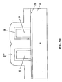
- FIGS. 10-14 specifically shows exemplary processing steps for forming an alternative CMOS diode with spaced apart first and second gate conductors 22 and 24 that are isolated from each other by a silicon oxide isolation structure 23'.
- FIG. 10 shows deposition of a blanket silicon oxide layer 27', instead of the blanket silicon nitride layer 27 as shown in FIG. 6 , over the entire structure including the first and second gate conductors 22 and 24.
- the blanket silicon oxide layer 27' is then patterned by conventional lithography and etching to form the silicon oxide isolation structure 23' between the first and second gate conductors 22 and 24 and the optional silicon oxide spacers 26' along sidewalls of the first and second gate conductors 22 and 24.
- additional silicon nitride spacers 26 can preferably be, but is not necessarily, formed along sidewalls of the silicon oxide spacers 26' by first depositing a blanket silicon nitride layer (not shown) followed by conventional lithographic and etching steps as described hereinabove. Note that if no silicon oxide spacers 26' are formed, then the silicon nitride spacers 26 are formed directly over sidewalls of the first and second gate conductors 22 and 24.
- First and second masked dopant implantation steps and the silicidation step, as described hereinabove, can then be carried out to implant n-type and p-type dopant species into the first and second gate conductors 22 and 24 and to form the n-doped and p-doped regions 12 and 14 as well as the surface silicide layers 12A, 14A, 22A, and 24A, as shown in FIGS. 13 and 14 .
- FIG. 15 is a SEM photograph of a portion of a CMOS diode that is fabricated according to the description hereinabove. Specifically, FIG. 15 shows a first gate conductor 22 and a second gate conductor 24 that are spaced apart from each other with a silicon nitride isolation structure 23 therebetween. Further, an oxide liner 25 is provided over the first and second gate conductors 22 and 24, and a silicon nitride cap layer 30 is formed over the entire CMOS diode.
Landscapes
- Metal-Oxide And Bipolar Metal-Oxide Semiconductor Integrated Circuits (AREA)
Claims (15)
- Halbleitereinheit, welche das Folgende umfasst:ein Halbleitersubstrat (10), welches einen ersten dotierten Bereich (12) einer Leitfähigkeit des n-Typs und einen zweiten dotierten Bereich (14) einer Leitfähigkeit des p-Typs aufweist, wobei in dem Raum dazwischen ein dritter dotierter Bereich (13) angeordnet ist, wobei der dritte dotierte Bereich eine Leitfähigkeit entweder des n- oder des p-Typs mit einer Dotierstoffkonzentration aufweist, die niedriger ist als die des ersten oder zweiten Bereichs; undeine Gate-Dielektrikums-Schicht (20), welche über dem Halbleitersubstrat angeordnet ist;wobei die Halbleitereinheit ferner das Folgende umfasst:einen ersten Gate-Leiter (22) einer Leitfähigkeit des n-Typs, welcher an die dielektrische Schicht in unmittelbarer Nachbarschaft zu dem ersten dotierten Bereich in dem Halbleitersubstrat angrenzt; undeinen zweiten Gate-Leiter (24) einer Leitfähigkeit des p-Typs, welcher an die dielektrische Schicht in unmittelbarer Nachbarschaft zu dem zweiten dotierten Bereich in dem Halbleitersubstrat angrenzt und welcher durch eine dazwischen angeordnete dielektrische Isolierungsstruktur (23) einen Abstand zu dem ersten Gate-Leiter aufweist und von diesem isoliert ist,wobei der erste, zweite und dritte dotierte Bereich und der erste und zweite Gate-Leiter so angeordnet und konstruiert sind, dass sie einen Anreicherungsbereich (16) und einen darunter angeordneten Verarmungsbereich (18) zwischen dem dritten dotierten Bereich und dem zweiten oder dem ersten dotierten Bereich bilden.
- Halbleitereinheit nach Anspruch 1, wobei:der dritte dotierte Bereich (13) eine Leitfähigkeit des n-Typs mit einer niedrigeren Dotierstoffkonzentration als der des ersten Bereichs (12) aufweist ; undder Anreicherungsbereich (16) und der darunter angeordnete Verarmungsbereich (18) sich zwischen dem dritten dotierten Bereich und dem zweiten dotierten Bereich (14) befinden.
- Halbleitereinheit nach Anspruch 1, wobei:der dritte dotierte Bereich (13) eine Leitfähigkeit des p-Typs mit einer niedrigeren Dotierstoffkonzentration als der des zweiten Bereichs (14) aufweist ; undder Anreicherungsbereich (16) und der darunter angeordnete Verarmungsbereich (18) sich zwischen dem dritten dotierten Bereich und dem ersten dotierten Bereich (12) befinden.
- Halbleitereinheit nach einem der Ansprüche 1 bis 3, wobei die dielektrische Isolierungsstruktur (23) ein dielektrisches Material umfasst, welches aus der Gruppe ausgewählt ist, die aus Oxiden, Nitriden und Oxynitriden besteht.
- Halbleitereinheit nach einem der Ansprüche 1 bis 3, wobei der erste (12) und zweite (14) dotierte Bereich und der erste (22) und zweite (24) Gate-Leiter jeweils eine Oberflächen-Silicidschicht umfassen.
- Halbleitereinheit nach einem der Ansprüche 1 bis 3, welche ferner einen oder mehrere dielektrische Abstandhalter (26) entlang einer oder mehreren Seitenwänden des ersten (22) und zweiten (24) Gate-Leiters umfasst.
- Halbleitereinheit nach Anspruch 6, wobei der eine oder die mehreren dielektrischen Abstandhalter (26) einen oder mehrere Oxid-Abstandhalter umfassen.
- Halbleitereinheit nach Anspruch 7, wobei der eine oder die mehreren dielektrischen Abstandhalter (26) ferner einen oder mehrere Nitrid-Abstandhalter umfassen.
- Halbleitereinheit nach einem der Ansprüche 1 bis 3, welche ferner eine dielektrische Deckschicht (27) über dem ersten (22) und zweiten (24) Gate-Leiter und dem Halbleitersubstrat (10) umfasst.
- Verfahren zum Bilden einer Halbleitereinheit, welches das Folgende umfasst:Bilden einer Gate-Dielektrikums-Schicht (20) über einem Halbleitersubstrat (10) mit einem darin angeordneten Wannenbereich einer Leitfähigkeit entweder des n- oder des p-Typs;Bilden eines ersten (22) und zweiten (24) Gate-Leiters, welche an die Gate-Dielektrikums-Schicht angrenzen, wobei der erste und zweite Gate-Leiter einen Abstand voneinander aufweisen;Bilden einer dielektrischen Isolierungsstruktur (23) zwischen dem ersten und zweiten Gate-Leiter;selektives Dotieren des ersten Gate-Leiters und eines ersten Bereichs (12) in dem Wannenbereich des Halbleitersubstrats mit einem Dotierstoff des n-Typs ; undselektives Dotieren des zweiten Gate-Leiters und eines zweiten Bereichs (14) in dem Wannenbereich des Halbleitersubstrats mit einem Dotierstoff des p-Typs, wobei der zweite Bereich einen Abstand von dem ersten Bereich aufweist, wodurch in dem Raum dazwischen ein dritter Bereich (13) in dem Wannenbereich definiert wird,wobei der erste, zweite und dritte dotierte Bereich und der erste und zweite Gate-Leiter so angeordnet und konstruiert sind, dass sie einen Anreicherungsbereich (16) und einen darunter angeordneten Verarmungsbereich (18) zwischen dem dritten Bereich und dem zweiten oder dem ersten Bereich bilden.
- Verfahren nach Anspruch 10, wobei der Wannenbereich des Halbleitersubstrats (10) eine Leitfähigkeit des n-Typs aufweist, der Anreicherungsbereich (16) zwischen dem dritten Bereich (13) und dem zweiten Bereich (14) gebildet wird und der Anreicherungsbereich eine Breite aufweist, welche mit der des zweiten Gate-Leiters (24) in positiver Wechselbeziehung steht.
- Verfahren nach Anspruch 10, wobei der Wannenbereich des Halbleitersubstrats eine Leitfähigkeit des p-Typs aufweist, der Anreicherungsbereich (16) zwischen dem dritten Bereich (13) und dem ersten Bereich (12) gebildet wird und der Anreicherungsbereich eine Breite aufweist, welche mit der des ersten Gate-Leiters (22) in positiver Wechselbeziehung steht.
- Verfahren nach Anspruch 10, wobei die dielektrische Isolierungsstruktur (23) durch Aufbringen einer überdeckenden dielektrischen Schicht (27) sowohl über dem ersten (22) als auch über dem zweiten (24) Gate-Leiter, gefolgt vom Strukturieren mindestens eines Abschnitts der überdeckenden dielektrischen Schicht zu mindestens der dielektrischen Isolierungsstruktur gebildet wird.
- Verfahren nach Anspruch 13, wobei weitere Abschnitte der überdeckenden dielektrischen Schicht (27) zu einem oder mehreren dielektrischen Abstandhaltern (26) entlang einer oder mehreren Seitenwänden des ersten (22) und zweiten (24) Gate-Leiters strukturiert werden.
- Verfahren nach Anspruch 13, wobei die dielektrische Isolierungsstruktur (23) ein dielektrisches Material umfasst, welches aus der Gruppe ausgewählt ist, die aus Oxiden, Nitriden und Oxynitriden besteht.
Applications Claiming Priority (2)
| Application Number | Priority Date | Filing Date | Title |
|---|---|---|---|
| US11/380,278 US7737500B2 (en) | 2006-04-26 | 2006-04-26 | CMOS diodes with dual gate conductors, and methods for forming the same |
| PCT/US2007/067361 WO2007127770A2 (en) | 2006-04-26 | 2007-04-25 | Improved cmos diodes with dual gate conductors, and methods for forming the same |
Publications (3)
| Publication Number | Publication Date |
|---|---|
| EP2020029A2 EP2020029A2 (de) | 2009-02-04 |
| EP2020029A4 EP2020029A4 (de) | 2009-09-09 |
| EP2020029B1 true EP2020029B1 (de) | 2012-08-29 |
Family
ID=38647542
Family Applications (1)
| Application Number | Title | Priority Date | Filing Date |
|---|---|---|---|
| EP07761243A Not-in-force EP2020029B1 (de) | 2006-04-26 | 2007-04-25 | Verbesserte cmos-dioden mit doppelgate-leitern und verfahren zu ihrer herstellung |
Country Status (5)
| Country | Link |
|---|---|
| US (2) | US7737500B2 (de) |
| EP (1) | EP2020029B1 (de) |
| CN (1) | CN101427370B (de) |
| TW (1) | TW200807727A (de) |
| WO (1) | WO2007127770A2 (de) |
Families Citing this family (15)
| Publication number | Priority date | Publication date | Assignee | Title |
|---|---|---|---|---|
| KR100757654B1 (ko) * | 2006-05-26 | 2007-09-10 | 매그나칩 반도체 유한회사 | 시모스 이미지 센서 및 그 제조 방법 |
| US8110465B2 (en) | 2007-07-30 | 2012-02-07 | International Business Machines Corporation | Field effect transistor having an asymmetric gate electrode |
| US7951678B2 (en) * | 2008-08-12 | 2011-05-31 | International Business Machines Corporation | Metal-gate high-k reference structure |
| US8405123B2 (en) * | 2008-10-27 | 2013-03-26 | National Semiconductor Corporation | Split-gate ESD diodes with elevated voltage tolerance |
| CN101710584B (zh) * | 2009-12-01 | 2011-05-11 | 中国科学院上海微系统与信息技术研究所 | 混合材料积累型全包围栅cmos场效应晶体管 |
| JP5582030B2 (ja) * | 2010-12-28 | 2014-09-03 | 富士通セミコンダクター株式会社 | Mosトランジスタおよびその製造方法 |
| US8264214B1 (en) * | 2011-03-18 | 2012-09-11 | Altera Corporation | Very low voltage reference circuit |
| WO2013014547A1 (en) * | 2011-07-22 | 2013-01-31 | International Business Machines Corporation | Tunnel field-effect transistor |
| GB2506831B (en) * | 2011-08-16 | 2015-09-02 | Fox Int Group Ltd | A method feeder |
| TWI473146B (zh) * | 2012-09-18 | 2015-02-11 | Macronix Int Co Ltd | 閘極結構及其製造方法 |
| JP5784652B2 (ja) * | 2013-02-14 | 2015-09-24 | 株式会社東芝 | 半導体装置 |
| US8932920B2 (en) | 2013-05-29 | 2015-01-13 | International Business Machines Corporation | Self-aligned gate electrode diffusion barriers |
| US9287406B2 (en) | 2013-06-06 | 2016-03-15 | Macronix International Co., Ltd. | Dual-mode transistor devices and methods for operating same |
| US9640645B2 (en) * | 2013-09-05 | 2017-05-02 | Taiwan Semiconductor Manufacturing Company Limited | Semiconductor device with silicide |
| KR20230068196A (ko) * | 2021-11-10 | 2023-05-17 | 삼성전자주식회사 | 반도체 소자 및 복수 개의 반도체 소자를 포함하는 멀티플렉서 |
Family Cites Families (20)
| Publication number | Priority date | Publication date | Assignee | Title |
|---|---|---|---|---|
| US5468669A (en) * | 1993-10-29 | 1995-11-21 | At&T Corp. | Integrated circuit fabrication |
| US5382818A (en) | 1993-12-08 | 1995-01-17 | Philips Electronics North America Corporation | Lateral semiconductor-on-insulator (SOI) semiconductor device having a buried diode |
| US5759886A (en) * | 1995-09-28 | 1998-06-02 | National Semiconductor Corporation | Method for forming a layer of metal silicide over the gates of a surface-channel CMOS device |
| US5683941A (en) * | 1996-07-02 | 1997-11-04 | National Semiconductor Corporation | Self-aligned polycide process that utilizes a planarized layer of material to expose polysilicon structures to a subsequently deposited metal layer that is reacted to form the metal silicide |
| US6093623A (en) | 1998-08-04 | 2000-07-25 | Micron Technology, Inc. | Methods for making silicon-on-insulator structures |
| US6015993A (en) | 1998-08-31 | 2000-01-18 | International Business Machines Corporation | Semiconductor diode with depleted polysilicon gate structure and method |
| US6423613B1 (en) | 1998-11-10 | 2002-07-23 | Micron Technology, Inc. | Low temperature silicon wafer bond process with bulk material bond strength |
| US6255198B1 (en) | 1998-11-24 | 2001-07-03 | North Carolina State University | Methods of fabricating gallium nitride microelectronic layers on silicon layers and gallium nitride microelectronic structures formed thereby |
| US6759315B1 (en) * | 1999-01-04 | 2004-07-06 | International Business Machines Corporation | Method for selective trimming of gate structures and apparatus formed thereby |
| US6429482B1 (en) | 2000-06-08 | 2002-08-06 | International Business Machines Corporation | Halo-free non-rectifying contact on chip with halo source/drain diffusion |
| US6559470B2 (en) | 2000-06-22 | 2003-05-06 | Progressed Technologies, Inc. | Negative differential resistance field effect transistor (NDR-FET) and circuits using the same |
| US6894324B2 (en) | 2001-02-15 | 2005-05-17 | United Microelectronics Corp. | Silicon-on-insulator diodes and ESD protection circuits |
| US6852167B2 (en) | 2001-03-01 | 2005-02-08 | Micron Technology, Inc. | Methods, systems, and apparatus for uniform chemical-vapor depositions |
| US6956262B1 (en) | 2001-12-21 | 2005-10-18 | Synopsys Inc. | Charge trapping pull up element |
| US6864104B2 (en) | 2002-06-28 | 2005-03-08 | Progressant Technologies, Inc. | Silicon on insulator (SOI) negative differential resistance (NDR) based memory device with reduced body effects |
| US6912151B2 (en) | 2002-06-28 | 2005-06-28 | Synopsys, Inc. | Negative differential resistance (NDR) based memory device with reduced body effects |
| US6768156B1 (en) | 2003-02-10 | 2004-07-27 | Micron Technology, Inc. | Non-volatile random access memory cells associated with thin film constructions |
| US7555173B2 (en) | 2003-04-09 | 2009-06-30 | Cornell Research Foundation, Inc. | Electro-optic modulator on rib waveguide |
| US20050035410A1 (en) * | 2003-08-15 | 2005-02-17 | Yee-Chia Yeo | Semiconductor diode with reduced leakage |
| US7166904B2 (en) | 2004-02-03 | 2007-01-23 | International Business Machines Corporation | Structure and method for local resistor element in integrated circuit technology |
-
2006
- 2006-04-26 US US11/380,278 patent/US7737500B2/en not_active Expired - Fee Related
-
2007
- 2007-04-16 TW TW096113385A patent/TW200807727A/zh unknown
- 2007-04-25 EP EP07761243A patent/EP2020029B1/de not_active Not-in-force
- 2007-04-25 WO PCT/US2007/067361 patent/WO2007127770A2/en not_active Ceased
- 2007-04-25 CN CN2007800142068A patent/CN101427370B/zh not_active Expired - Fee Related
-
2010
- 2010-06-14 US US12/814,930 patent/US8222702B2/en not_active Expired - Fee Related
Also Published As
| Publication number | Publication date |
|---|---|
| EP2020029A4 (de) | 2009-09-09 |
| US7737500B2 (en) | 2010-06-15 |
| US20070252212A1 (en) | 2007-11-01 |
| WO2007127770A2 (en) | 2007-11-08 |
| US8222702B2 (en) | 2012-07-17 |
| EP2020029A2 (de) | 2009-02-04 |
| WO2007127770A3 (en) | 2008-11-13 |
| TW200807727A (en) | 2008-02-01 |
| US20100252881A1 (en) | 2010-10-07 |
| CN101427370B (zh) | 2011-03-30 |
| CN101427370A (zh) | 2009-05-06 |
Similar Documents
| Publication | Publication Date | Title |
|---|---|---|
| EP2020029B1 (de) | Verbesserte cmos-dioden mit doppelgate-leitern und verfahren zu ihrer herstellung | |
| US6911383B2 (en) | Hybrid planar and finFET CMOS devices | |
| US9905476B2 (en) | Alternative threshold voltage scheme via direct metal gate patterning for high performance CMOS FinFETs | |
| US7741164B2 (en) | Method for fabricating SOI device | |
| KR101185685B1 (ko) | Cmos 프로세스를 위한 금속 게이트 트랜지스터 및 제조방법 | |
| US20090218625A1 (en) | Modified Hybrid Orientation Technology | |
| EP1949435A1 (de) | STRUKTUR UND VERFAHREN ZUR VERGRÖßERUNG DER VERSPANNUNGSERWEITERUNG MIT ABSTANDSSCHICHTLOSEM FET- UND DOPPEL-LINER-PROZESS | |
| US9972545B2 (en) | System and method for a field-effect transistor with dual vertical gates | |
| US12402376B2 (en) | High-voltage nano-sheet transistor | |
| US20190305132A1 (en) | Method and structure of improving contact resistance for passive and long channel devices | |
| US7919379B2 (en) | Dielectric spacer removal | |
| US20080096342A1 (en) | Cmos circuits including a passive element having a low end resistance | |
| KR102638419B1 (ko) | 입력/출력 디바이스 | |
| US20060157796A1 (en) | Semiconductor device having dual gate electrode and related method of formation | |
| EP1225628B1 (de) | Herstellung eines CMOS Kondensators | |
| US9793161B2 (en) | Methods for contact formation for 10 nanometers and beyond with minimal mask counts | |
| US20060228862A1 (en) | Fet design with long gate and dense pitch | |
| US20070221999A1 (en) | Semiconductor devices and methods of manufacture thereof | |
| US7465623B2 (en) | Methods for fabricating a semiconductor device on an SOI substrate | |
| US10326019B2 (en) | Fully-depleted CMOS transistors with U-shaped channel | |
| US11322602B2 (en) | Vertical field-effect transistor (VFET) devices and methods of forming the same | |
| TW201427019A (zh) | 半導體結構及積體電路之製造方法 |
Legal Events
| Date | Code | Title | Description |
|---|---|---|---|
| PUAI | Public reference made under article 153(3) epc to a published international application that has entered the european phase |
Free format text: ORIGINAL CODE: 0009012 |
|
| 17P | Request for examination filed |
Effective date: 20081125 |
|
| AK | Designated contracting states |
Kind code of ref document: A2 Designated state(s): AT BE BG CH CY CZ DE DK EE ES FI FR GB GR HU IE IS IT LI LT LU LV MC MT NL PL PT RO SE SI SK TR |
|
| AX | Request for extension of the european patent |
Extension state: AL BA HR MK RS |
|
| RIN1 | Information on inventor provided before grant (corrected) |
Inventor name: ONSONGO, DAVID, M.C/O IBM UNITED KINGDOM LIMITED Inventor name: RAUSCH, WERNER Inventor name: YANG, HAINING, S. |
|
| A4 | Supplementary search report drawn up and despatched |
Effective date: 20090810 |
|
| RIC1 | Information provided on ipc code assigned before grant |
Ipc: H01L 21/329 20060101ALI20090804BHEP Ipc: H01L 23/62 20060101AFI20080204BHEP Ipc: H01L 29/78 20060101ALI20090804BHEP Ipc: H01L 29/739 20060101ALI20090804BHEP |
|
| REG | Reference to a national code |
Ref country code: DE Ref legal event code: R079 Ref document number: 602007025134 Country of ref document: DE Free format text: PREVIOUS MAIN CLASS: H01L0023620000 Ipc: H01L0029660000 |
|
| RIC1 | Information provided on ipc code assigned before grant |
Ipc: H01L 29/739 20060101ALI20120322BHEP Ipc: H01L 29/66 20060101AFI20120322BHEP Ipc: H01L 29/78 20060101ALI20120322BHEP Ipc: H01L 23/62 20060101ALI20120322BHEP |
|
| GRAP | Despatch of communication of intention to grant a patent |
Free format text: ORIGINAL CODE: EPIDOSNIGR1 |
|
| DAX | Request for extension of the european patent (deleted) | ||
| GRAS | Grant fee paid |
Free format text: ORIGINAL CODE: EPIDOSNIGR3 |
|
| GRAA | (expected) grant |
Free format text: ORIGINAL CODE: 0009210 |
|
| AK | Designated contracting states |
Kind code of ref document: B1 Designated state(s): AT BE BG CH CY CZ DE DK EE ES FI FR GB GR HU IE IS IT LI LT LU LV MC MT NL PL PT RO SE SI SK TR |
|
| REG | Reference to a national code |
Ref country code: GB Ref legal event code: FG4D |
|
| REG | Reference to a national code |
Ref country code: CH Ref legal event code: NV Representative=s name: IBM RESEARCH GMBH ZURICH RESEARCH LABORATORY INTEL Ref country code: CH Ref legal event code: EP |
|
| REG | Reference to a national code |
Ref country code: AT Ref legal event code: REF Ref document number: 573465 Country of ref document: AT Kind code of ref document: T Effective date: 20120915 |
|
| REG | Reference to a national code |
Ref country code: IE Ref legal event code: FG4D |
|
| REG | Reference to a national code |
Ref country code: DE Ref legal event code: R096 Ref document number: 602007025134 Country of ref document: DE Effective date: 20121025 |
|
| REG | Reference to a national code |
Ref country code: GB Ref legal event code: 746 Effective date: 20121029 |
|
| REG | Reference to a national code |
Ref country code: DE Ref legal event code: R084 Ref document number: 602007025134 Country of ref document: DE Effective date: 20120921 |
|
| REG | Reference to a national code |
Ref country code: AT Ref legal event code: MK05 Ref document number: 573465 Country of ref document: AT Kind code of ref document: T Effective date: 20120829 |
|
| REG | Reference to a national code |
Ref country code: NL Ref legal event code: VDEP Effective date: 20120829 |
|
| REG | Reference to a national code |
Ref country code: LT Ref legal event code: MG4D Effective date: 20120829 |
|
| PG25 | Lapsed in a contracting state [announced via postgrant information from national office to epo] |
Ref country code: AT Free format text: LAPSE BECAUSE OF FAILURE TO SUBMIT A TRANSLATION OF THE DESCRIPTION OR TO PAY THE FEE WITHIN THE PRESCRIBED TIME-LIMIT Effective date: 20120829 Ref country code: IS Free format text: LAPSE BECAUSE OF FAILURE TO SUBMIT A TRANSLATION OF THE DESCRIPTION OR TO PAY THE FEE WITHIN THE PRESCRIBED TIME-LIMIT Effective date: 20121229 Ref country code: LT Free format text: LAPSE BECAUSE OF FAILURE TO SUBMIT A TRANSLATION OF THE DESCRIPTION OR TO PAY THE FEE WITHIN THE PRESCRIBED TIME-LIMIT Effective date: 20120829 Ref country code: FI Free format text: LAPSE BECAUSE OF FAILURE TO SUBMIT A TRANSLATION OF THE DESCRIPTION OR TO PAY THE FEE WITHIN THE PRESCRIBED TIME-LIMIT Effective date: 20120829 Ref country code: CY Free format text: LAPSE BECAUSE OF FAILURE TO SUBMIT A TRANSLATION OF THE DESCRIPTION OR TO PAY THE FEE WITHIN THE PRESCRIBED TIME-LIMIT Effective date: 20120829 |
|
| PG25 | Lapsed in a contracting state [announced via postgrant information from national office to epo] |
Ref country code: LV Free format text: LAPSE BECAUSE OF FAILURE TO SUBMIT A TRANSLATION OF THE DESCRIPTION OR TO PAY THE FEE WITHIN THE PRESCRIBED TIME-LIMIT Effective date: 20120829 Ref country code: SE Free format text: LAPSE BECAUSE OF FAILURE TO SUBMIT A TRANSLATION OF THE DESCRIPTION OR TO PAY THE FEE WITHIN THE PRESCRIBED TIME-LIMIT Effective date: 20120829 Ref country code: GR Free format text: LAPSE BECAUSE OF FAILURE TO SUBMIT A TRANSLATION OF THE DESCRIPTION OR TO PAY THE FEE WITHIN THE PRESCRIBED TIME-LIMIT Effective date: 20121130 Ref country code: SI Free format text: LAPSE BECAUSE OF FAILURE TO SUBMIT A TRANSLATION OF THE DESCRIPTION OR TO PAY THE FEE WITHIN THE PRESCRIBED TIME-LIMIT Effective date: 20120829 Ref country code: PT Free format text: LAPSE BECAUSE OF FAILURE TO SUBMIT A TRANSLATION OF THE DESCRIPTION OR TO PAY THE FEE WITHIN THE PRESCRIBED TIME-LIMIT Effective date: 20121231 Ref country code: BE Free format text: LAPSE BECAUSE OF FAILURE TO SUBMIT A TRANSLATION OF THE DESCRIPTION OR TO PAY THE FEE WITHIN THE PRESCRIBED TIME-LIMIT Effective date: 20120829 |
|
| PG25 | Lapsed in a contracting state [announced via postgrant information from national office to epo] |
Ref country code: NL Free format text: LAPSE BECAUSE OF FAILURE TO SUBMIT A TRANSLATION OF THE DESCRIPTION OR TO PAY THE FEE WITHIN THE PRESCRIBED TIME-LIMIT Effective date: 20120829 Ref country code: ES Free format text: LAPSE BECAUSE OF FAILURE TO SUBMIT A TRANSLATION OF THE DESCRIPTION OR TO PAY THE FEE WITHIN THE PRESCRIBED TIME-LIMIT Effective date: 20121210 Ref country code: DK Free format text: LAPSE BECAUSE OF FAILURE TO SUBMIT A TRANSLATION OF THE DESCRIPTION OR TO PAY THE FEE WITHIN THE PRESCRIBED TIME-LIMIT Effective date: 20120829 Ref country code: CZ Free format text: LAPSE BECAUSE OF FAILURE TO SUBMIT A TRANSLATION OF THE DESCRIPTION OR TO PAY THE FEE WITHIN THE PRESCRIBED TIME-LIMIT Effective date: 20120829 Ref country code: EE Free format text: LAPSE BECAUSE OF FAILURE TO SUBMIT A TRANSLATION OF THE DESCRIPTION OR TO PAY THE FEE WITHIN THE PRESCRIBED TIME-LIMIT Effective date: 20120829 Ref country code: RO Free format text: LAPSE BECAUSE OF FAILURE TO SUBMIT A TRANSLATION OF THE DESCRIPTION OR TO PAY THE FEE WITHIN THE PRESCRIBED TIME-LIMIT Effective date: 20120829 |
|
| PG25 | Lapsed in a contracting state [announced via postgrant information from national office to epo] |
Ref country code: PL Free format text: LAPSE BECAUSE OF FAILURE TO SUBMIT A TRANSLATION OF THE DESCRIPTION OR TO PAY THE FEE WITHIN THE PRESCRIBED TIME-LIMIT Effective date: 20120829 Ref country code: IT Free format text: LAPSE BECAUSE OF FAILURE TO SUBMIT A TRANSLATION OF THE DESCRIPTION OR TO PAY THE FEE WITHIN THE PRESCRIBED TIME-LIMIT Effective date: 20120829 Ref country code: SK Free format text: LAPSE BECAUSE OF FAILURE TO SUBMIT A TRANSLATION OF THE DESCRIPTION OR TO PAY THE FEE WITHIN THE PRESCRIBED TIME-LIMIT Effective date: 20120829 |
|
| PLBE | No opposition filed within time limit |
Free format text: ORIGINAL CODE: 0009261 |
|
| STAA | Information on the status of an ep patent application or granted ep patent |
Free format text: STATUS: NO OPPOSITION FILED WITHIN TIME LIMIT |
|
| PG25 | Lapsed in a contracting state [announced via postgrant information from national office to epo] |
Ref country code: BG Free format text: LAPSE BECAUSE OF FAILURE TO SUBMIT A TRANSLATION OF THE DESCRIPTION OR TO PAY THE FEE WITHIN THE PRESCRIBED TIME-LIMIT Effective date: 20121129 |
|
| 26N | No opposition filed |
Effective date: 20130530 |
|
| REG | Reference to a national code |
Ref country code: DE Ref legal event code: R097 Ref document number: 602007025134 Country of ref document: DE Effective date: 20130530 |
|
| PG25 | Lapsed in a contracting state [announced via postgrant information from national office to epo] |
Ref country code: MC Free format text: LAPSE BECAUSE OF FAILURE TO SUBMIT A TRANSLATION OF THE DESCRIPTION OR TO PAY THE FEE WITHIN THE PRESCRIBED TIME-LIMIT Effective date: 20120829 |
|
| REG | Reference to a national code |
Ref country code: CH Ref legal event code: PL |
|
| REG | Reference to a national code |
Ref country code: IE Ref legal event code: MM4A |
|
| PG25 | Lapsed in a contracting state [announced via postgrant information from national office to epo] |
Ref country code: CH Free format text: LAPSE BECAUSE OF NON-PAYMENT OF DUE FEES Effective date: 20130430 Ref country code: LI Free format text: LAPSE BECAUSE OF NON-PAYMENT OF DUE FEES Effective date: 20130430 |
|
| REG | Reference to a national code |
Ref country code: FR Ref legal event code: ST Effective date: 20131231 |
|
| PG25 | Lapsed in a contracting state [announced via postgrant information from national office to epo] |
Ref country code: FR Free format text: LAPSE BECAUSE OF NON-PAYMENT OF DUE FEES Effective date: 20130430 |
|
| PG25 | Lapsed in a contracting state [announced via postgrant information from national office to epo] |
Ref country code: IE Free format text: LAPSE BECAUSE OF NON-PAYMENT OF DUE FEES Effective date: 20130425 |
|
| PG25 | Lapsed in a contracting state [announced via postgrant information from national office to epo] |
Ref country code: MT Free format text: LAPSE BECAUSE OF FAILURE TO SUBMIT A TRANSLATION OF THE DESCRIPTION OR TO PAY THE FEE WITHIN THE PRESCRIBED TIME-LIMIT Effective date: 20120829 |
|
| PG25 | Lapsed in a contracting state [announced via postgrant information from national office to epo] |
Ref country code: TR Free format text: LAPSE BECAUSE OF FAILURE TO SUBMIT A TRANSLATION OF THE DESCRIPTION OR TO PAY THE FEE WITHIN THE PRESCRIBED TIME-LIMIT Effective date: 20120829 |
|
| PG25 | Lapsed in a contracting state [announced via postgrant information from national office to epo] |
Ref country code: LU Free format text: LAPSE BECAUSE OF NON-PAYMENT OF DUE FEES Effective date: 20130425 Ref country code: HU Free format text: LAPSE BECAUSE OF FAILURE TO SUBMIT A TRANSLATION OF THE DESCRIPTION OR TO PAY THE FEE WITHIN THE PRESCRIBED TIME-LIMIT; INVALID AB INITIO Effective date: 20070425 |
|
| PGFP | Annual fee paid to national office [announced via postgrant information from national office to epo] |
Ref country code: GB Payment date: 20150428 Year of fee payment: 9 |
|
| REG | Reference to a national code |
Ref country code: DE Ref legal event code: R082 Ref document number: 602007025134 Country of ref document: DE Representative=s name: RICHARDT PATENTANWAELTE PARTG MBB, DE Ref country code: DE Ref legal event code: R081 Ref document number: 602007025134 Country of ref document: DE Owner name: GLOBALFOUNDRIES US 2 LLC (N.D.GES.DES STAATES , US Free format text: FORMER OWNER: INTERNATIONAL BUSINESS MACHINES CORPORATION, ARMONK, N.Y., US Ref country code: DE Ref legal event code: R081 Ref document number: 602007025134 Country of ref document: DE Owner name: GLOBALFOUNDRIES INC., KY Free format text: FORMER OWNER: INTERNATIONAL BUSINESS MACHINES CORPORATION, ARMONK, N.Y., US |
|
| REG | Reference to a national code |
Ref country code: DE Ref legal event code: R081 Ref document number: 602007025134 Country of ref document: DE Owner name: GLOBALFOUNDRIES INC., KY Free format text: FORMER OWNER: GLOBALFOUNDRIES US 2 LLC (N.D.GES.DES STAATES DELAWARE), HOPEWELL JUNCTION, N.Y., US Ref country code: DE Ref legal event code: R082 Ref document number: 602007025134 Country of ref document: DE Representative=s name: RICHARDT PATENTANWAELTE PARTG MBB, DE |
|
| GBPC | Gb: european patent ceased through non-payment of renewal fee |
Effective date: 20160425 |
|
| PG25 | Lapsed in a contracting state [announced via postgrant information from national office to epo] |
Ref country code: GB Free format text: LAPSE BECAUSE OF NON-PAYMENT OF DUE FEES Effective date: 20160425 |
|
| PGFP | Annual fee paid to national office [announced via postgrant information from national office to epo] |
Ref country code: DE Payment date: 20180410 Year of fee payment: 12 |
|
| REG | Reference to a national code |
Ref country code: DE Ref legal event code: R119 Ref document number: 602007025134 Country of ref document: DE |
|
| PG25 | Lapsed in a contracting state [announced via postgrant information from national office to epo] |
Ref country code: DE Free format text: LAPSE BECAUSE OF NON-PAYMENT OF DUE FEES Effective date: 20191101 |