EP2020620A2 - Einstellungsverfahren, Belichtungsverfahren, Verfahren zur Herstellung einer Vorrichtung und Belichtungsvorrichtung - Google Patents
Einstellungsverfahren, Belichtungsverfahren, Verfahren zur Herstellung einer Vorrichtung und Belichtungsvorrichtung Download PDFInfo
- Publication number
- EP2020620A2 EP2020620A2 EP08161469A EP08161469A EP2020620A2 EP 2020620 A2 EP2020620 A2 EP 2020620A2 EP 08161469 A EP08161469 A EP 08161469A EP 08161469 A EP08161469 A EP 08161469A EP 2020620 A2 EP2020620 A2 EP 2020620A2
- Authority
- EP
- European Patent Office
- Prior art keywords
- light
- optical system
- polarization state
- reticle
- projection optical
- Prior art date
- Legal status (The legal status is an assumption and is not a legal conclusion. Google has not performed a legal analysis and makes no representation as to the accuracy of the status listed.)
- Withdrawn
Links
Images




Classifications
-
- G—PHYSICS
- G03—PHOTOGRAPHY; CINEMATOGRAPHY; ANALOGOUS TECHNIQUES USING WAVES OTHER THAN OPTICAL WAVES; ELECTROGRAPHY; HOLOGRAPHY
- G03F—PHOTOMECHANICAL PRODUCTION OF TEXTURED OR PATTERNED SURFACES, e.g. FOR PRINTING, FOR PROCESSING OF SEMICONDUCTOR DEVICES; MATERIALS THEREFOR; ORIGINALS THEREFOR; APPARATUS SPECIALLY ADAPTED THEREFOR
- G03F7/00—Photomechanical, e.g. photolithographic, production of textured or patterned surfaces, e.g. printing surfaces; Materials therefor, e.g. comprising photoresists; Apparatus specially adapted therefor
- G03F7/70—Microphotolithographic exposure; Apparatus therefor
- G03F7/70483—Information management; Active and passive control; Testing; Wafer monitoring, e.g. pattern monitoring
- G03F7/7055—Exposure light control in all parts of the microlithographic apparatus, e.g. pulse length control or light interruption
- G03F7/70566—Polarisation control
-
- G—PHYSICS
- G01—MEASURING; TESTING
- G01J—MEASUREMENT OF INTENSITY, VELOCITY, SPECTRAL CONTENT, POLARISATION, PHASE OR PULSE CHARACTERISTICS OF INFRARED, VISIBLE OR ULTRAVIOLET LIGHT; COLORIMETRY; RADIATION PYROMETRY
- G01J4/00—Measuring polarisation of light
- G01J4/04—Polarimeters using electric detection means
-
- G—PHYSICS
- G03—PHOTOGRAPHY; CINEMATOGRAPHY; ANALOGOUS TECHNIQUES USING WAVES OTHER THAN OPTICAL WAVES; ELECTROGRAPHY; HOLOGRAPHY
- G03F—PHOTOMECHANICAL PRODUCTION OF TEXTURED OR PATTERNED SURFACES, e.g. FOR PRINTING, FOR PROCESSING OF SEMICONDUCTOR DEVICES; MATERIALS THEREFOR; ORIGINALS THEREFOR; APPARATUS SPECIALLY ADAPTED THEREFOR
- G03F7/00—Photomechanical, e.g. photolithographic, production of textured or patterned surfaces, e.g. printing surfaces; Materials therefor, e.g. comprising photoresists; Apparatus specially adapted therefor
- G03F7/70—Microphotolithographic exposure; Apparatus therefor
- G03F7/70058—Mask illumination systems
- G03F7/70191—Optical correction elements, filters or phase plates for controlling intensity, wavelength, polarisation, phase or the like
-
- G—PHYSICS
- G03—PHOTOGRAPHY; CINEMATOGRAPHY; ANALOGOUS TECHNIQUES USING WAVES OTHER THAN OPTICAL WAVES; ELECTROGRAPHY; HOLOGRAPHY
- G03F—PHOTOMECHANICAL PRODUCTION OF TEXTURED OR PATTERNED SURFACES, e.g. FOR PRINTING, FOR PROCESSING OF SEMICONDUCTOR DEVICES; MATERIALS THEREFOR; ORIGINALS THEREFOR; APPARATUS SPECIALLY ADAPTED THEREFOR
- G03F7/00—Photomechanical, e.g. photolithographic, production of textured or patterned surfaces, e.g. printing surfaces; Materials therefor, e.g. comprising photoresists; Apparatus specially adapted therefor
- G03F7/70—Microphotolithographic exposure; Apparatus therefor
- G03F7/708—Construction of apparatus, e.g. environment aspects, hygiene aspects or materials
- G03F7/7085—Detection arrangement, e.g. detectors of apparatus alignment possibly mounted on wafers, exposure dose, photo-cleaning flux, stray light, thermal load
Definitions
- the present invention relates to an adjustment method, an exposure method, a device manufacturing method, and an exposure apparatus.
- NA numerical aperture
- high NA imaging There are three important factors in determining the exposure performance of a projection exposure apparatus: resolution, overlay accuracy, and throughput.
- resolution is especially attracting attention in relation with the development of increased numerical aperture (NA), which has become feasible with the use of an immersion projection optical system.
- NA numerical aperture
- Increased NA in a projection optical system leads to an increased angle between the perpendicular to an image plane and the traveling direction of incident light. This is referred to as high NA imaging.
- exposure light contains both s-polarized light and p-polarized light, then a light intensity distribution with inferior contrast is formed compared to when exposure light contains only s-polarized light. If the percentage of p-polarized light increases, then the contrast of a light intensity distribution on the image plane decreases, thus resulting in no transfer of the pattern.
- Controlling polarization of exposure light enables a light intensity distribution with sufficient contrast to be formed on an image plane. Accordingly, a finer pattern can be formed on the image plane.
- Polarization of exposure light can be controlled by controlling the polarization state on a pupil plane in an illumination optical system.
- the controlled polarization state is not always maintained on the image plane. This is because an optical system subsequent to the pupil plane in the illumination optical system or a projection optical system exerts an influence on the polarization state.
- an antireflection film may be formed on a lens or a high-reflectance film may be formed on a reflection mirror.
- the transmittance and reflectance of these films depend on a polarization direction.
- quartz or fluorite may be used as a lens material.
- Such a member causes a change in polarization state due to its birefringence.
- birefringence of the lens material may be changed.
- Japanese Patent Application Laid-Open No. 2007-59566 discusses an exposure apparatus that is capable of measuring the polarization state of an illumination optical system or a projection optical system.
- the exposure apparatus discussed in Japanese Patent Application Laid-Open No. 2007-59566 does not measure the polarization state of an illumination optical system or a projection optical system in a state where a reticle is set on a reticle stage. In other words, the exposure apparatus does not measure the polarization state in a state where the reticle is located between the illumination optical system and the projection optical system. Since actual exposure is performed with the reticle set between the illumination optical system and the projection optical system, the polarization state may be changed due to the birefringence of the reticle itself or to the stress birefringence caused when the reticle is held. Accordingly, although the exposure apparatus discussed in Japanese Patent Application Laid-Open No. 2007-59566 measures the polarization state of the illumination optical system or the projection optical system, the measured polarization state is not the polarization state under the actual exposure conditions.
- the present invention is directed to an adjustment method for adjusting illumination conditions by measuring a polarization state under an actual exposure condition.
- an exposure method as specified in claim 4 According to a second aspect of the present invention, there is provided an exposure method as specified in claim 4. According to a third aspect of the present invention, there is provided a manufacturing method as specified in claim 5. According to a fourth aspect of the present invention, there is provided an exposure apparatus as specified in claims 6 to8.
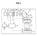
- Fig. 1 is a block diagram illustrating a configuration of an exposure apparatus according to an exemplary embodiment of the present invention.
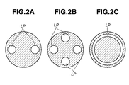
- Figs. 2A through 2C each illustrate an example of effective light source distribution formed by a beam shaping optical system of the exposure apparatus illustrated in Fig. 1 .
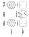
- Figs. 3A through 3C illustrate a polarization state before and after light passes through a phase plate of the exposure apparatus illustrated in Fig. 1 .
- Figs. 4A and 4B illustrate a relation between a fast-axis direction of the phase plate of the exposure apparatus illustrated in Fig. 1 and a polarization state of effective light source distribution.
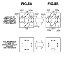
- Figs. 5A and 5B illustrate a relation between a phase difference of the phase plate of the exposure apparatus illustrated in Fig. 1 and a polarization state of effective light source distribution.
- Figs. 6A through 6G each illustrate an example of a polarization state on a pupil plane in an illumination optical system of the exposure apparatus illustrated in Fig. 1 .
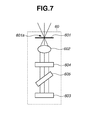
- Fig. 7 illustrates an example of a cross section of a measurement unit of the exposure apparatus illustrated in Fig. 1 .
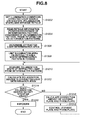
- Fig. 8 is a flowchart illustrating adjustment and exposure methods according to an exemplary embodiment of the present invention.
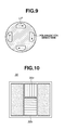
- Fig. 9 illustrates an example of an illumination condition (e.g., effective light source distribution and polarization state) of the exposure apparatus illustrated in Fig. 1 .
- an illumination condition e.g., effective light source distribution and polarization state
- Fig. 10 illustrates an example of a reticle used in the exposure apparatus illustrated in Fig. 1 .
- Fig. 11 illustrates an example of a polarization degree in a diffracted light determination area, which is calculated based on a polarization state of diffracted light from a determination pattern.
- Fig. 12 illustrates an example of an illumination condition (effective light source distribution and polarization state) of the exposure apparatus illustrated in Fig. 1 .
- Fig. 13 illustrates an example of a reticle used in the exposure apparatus illustrated in Fig. 1 .
- Fig. 15 is a flowchart illustrating an exposure method according to an exemplary embodiment of the present invention.
- Fig. 1 is a block diagram illustrating a configuration of an exposure apparatus according to an exemplary embodiment of the present invention.
- the exposure apparatus 1 is a projection exposure apparatus configured to project a pattern formed on a reticle (original plate) 30 onto a wafer (substrate) 50 using a step-and-scan method.
- a projection exposure apparatus using a step-and-repeat method or other exposure methods can also be used for the exposure apparatus 1.
- the exposure apparatus 1 includes a light source 10, an illumination optical system 20, a reticle stage 35 configured to support the reticle 30, a projection optical system 40, a wafer stage 55 configured to support the wafer 50, a measurement unit 60, a reading unit 70, a control unit 80, and a determination unit 90.
- Light emitted from the light source 10 is changed into a desired polarization state by a ⁇ /2 waveplate (phase plate) 201 and a phase plate (wave plate) 203, which will be described in detail below, and directed onto the reticle 30.
- a ⁇ /2 waveplate (phase plate) 201 and a phase plate (wave plate) 203 which will be described in detail below, and directed onto the reticle 30.
- light emitted from the light source 10 is described as approximately linear polarized light having an electric field vector oriented in a direction perpendicular to the drawing surface of Fig. 1 .
- the illumination optical system 20 is configured to illuminate the reticle 30 using light emitted from the light source 10.
- the illumination optical system 20 includes the ⁇ /2 waveplate 201, a beam shaping optical system 202, the phase plate 203, a fly-eye lens 204, a condenser lens 205, a masking blade 206, relay optical systems 207 and 209, and a folding mirror 208.
- An optical integrator for example, a microlens array can be used in place of the fly-eye lens 204.
- the ⁇ /2 waveplate 201 is controlled by the control unit 80, which will be described in detail below.
- the ⁇ /2 waveplate 201 is removably arranged in an optical path of the illumination optical system 20.
- the ⁇ /2 waveplate 201 collectively adjusts or changes the polarization state of light emitted from the light source 10.
- the ⁇ /2 waveplate 201 is arranged such that a fast-axis direction of the ⁇ /2 waveplate 201 is at an angle of 45 degrees with respect to the polarization direction of light emitted from the light source 10.
- the polarization state of light incident on an optical system of the subsequent stage can be either switched to linear polarized light having an electric field vector oriented in a direction perpendicular to the drawing sheet surface or to linear polarized light having an electric field vector oriented in a direction parallel to the drawing sheet surface.
- the ⁇ /2 waveplate 201 instead of configuring the ⁇ /2 waveplate 201 so that it can be set in the optical path or can be removed from the optical path, the ⁇ /2 waveplate 201 can be configured to be rotatable.
- the fast-axis direction of the ⁇ /2 waveplate 201 can be changed to a direction parallel to the polarization direction of light emitted from the light source 10 or to a direction at an angle of 45 degrees with respect to light emitted from the light source 10, and accordingly a similar effect can be obtained.
- the beam shaping optical system 202 functions as a light intensity generation unit configured to form a light intensity distribution (effective light source) on the pupil plane of the illumination optical system 20.
- the beam shaping optical system 202 provides, for example, effective light source distributions illustrated in Figs. 2A through 2C .
- the effective light source distribution illustrated in Fig. 2A is a dipole illumination having light portions LP in two off-axis areas on the pupil plane of the illumination optical system 20.
- the effective light source distribution illustrated in Fig. 2B is a quadrupole illumination having light portions LP in four off-axis areas on the pupil plane of the illumination optical system 20.
- the effective light source distribution illustrated in Fig. 2C is an annular illumination having a light portion LP in an off-axis annular area on the pupil plane of the illumination optical system 20.
- Figs. 2A through 2C illustrate examples of effective light source distributions formed by the beam shaping optical system 202.
- the phase plate 203 is controlled by the control unit 80, which will be described in detail below.
- the phase plate 203 is removably arranged in an optical path of the illumination optical system 20.
- the phase plate 203 functions as a polarization conversion unit configured to convert the polarization state of light emitted from the light source 10 and to form a desired polarization state on the pupil plane of the illumination optical system 20.
- the ⁇ /2 waveplate 201 collectively changes the polarization state of the light emitted from the light source 10
- the phase plate 203 makes partial adjustment to the polarization state on the pupil plane of the illumination optical system 20.
- the phase plate 203 does not necessarily perform adjustment of the polarization state on the pupil plane of the illumination optical system 20.
- the phase plate 203 may adjust the polarization state of light emitted from the light source 10 into a desired polarization state in a stage after the pupil plane of the illumination optical system 20 but before the reticle 30.
- Figs. 3A through 3C illustrate the polarization state of light before and after the phase plate 203.
- an effective light source distribution having a quadrupole illumination illustrated in Fig. 2B is formed by the beam shaping optical system 202.
- the light quantity distributions before and after the phase plate 203 in this case are illustrated in the upper portions of Fig. 3A and 3C .
- the light quantity distribution includes four light areas IA corresponding to the four light portions LP of the effective light source distribution illustrated in Fig. 2B .
- Light emitted from the light source 10 is converted into a uniform polarization state by the ⁇ /2 waveplate 201.
- the polarization state of light emitted from the light source 10 is converted into a polarization state having an electric field vector oriented in the vertical direction by the ⁇ /2 waveplate 201 as illustrated in Fig. 3A .
- four phase plates 203 or four phase plates 203a through 203d are arranged in four areas corresponding to the light areas IA (the light portions LP in the effective light source distribution area) illustrated in Fig. 3B .
- Each of the phase plates 203a and 203c is a ⁇ /2 waveplate with its fast axis oriented 45 degrees from the vertical direction.
- Each of the phase plates 203b and 203d is a ⁇ /2 waveplate with its fast axis oriented in the vertical direction.
- phase plate 203 When light emitted from the light source 10 passes through the phase plate 203 illustrated in Fig. 3B , since the polarization direction of light incident on the light areas IA on the upper and lower parts of the light quantity area is rotated 90 degrees by the phase plates 203a and 203c, the polarization state becomes as illustrated in Fig. 3C with the polarization direction in the horizontal direction. On the other hand, since the polarization direction of light incident on the light areas IA on the right and left parts of the light quantity area is parallel to the fast axis of the phase plates 203b and 203d, the polarization direction is unchanged, and thus the polarization state becomes as illustrated in Fig. 3C with the polarization direction in the vertical direction. Accordingly, light that has passed through the phase plate 203 has a quadrupole light intensity distribution with a different polarization state for each area.
- the phase plate 203 includes a rotation mechanism configured to allow independent rotation (drive) of the phase plates 203a through 203d. Since the control unit 80 is capable of controlling the rotation mechanism of the phase plate 203, partial adjustment of the polarization state on the pupil plane of the illumination optical system 20 can be independently performed.
- the fast-axis direction can be changed as illustrated in the upper portion of Fig. 4B .
- the polarization state of an area corresponding only to the phase plate 203c can be changed.
- the fast-axis directions of the phase plates 203a through 203d changeable for each area on the pupil plane of the illumination optical system 20
- the polarization direction of the effective light source distribution can be changed.
- Figs. 4A and 4B illustrate the fast-axis directions of the phase plates 203a through 203d and the polarization states of the effective light source distribution.
- phase plates 203a through 203d are rotated independently in each area in the effective light source distribution to adjust the polarization state, the entire phase plate 203 can also be rotated.
- the phase plate 203 includes phase plates 203e through 203h that can provide a phase difference of ⁇ ( ⁇ /2) in a field oscillation direction (plane of polarization) of incident light.
- the phase plate 203 if the phase plate 203 is in a state as illustrated in the upper portion of Fig. 5A , the effective light source distribution is in a polarization state as illustrated in the lower portion of Fig. 5A .
- the phase difference of the phase plate 203g is shifted from ⁇ ( ⁇ /2) (phase difference will be ⁇ ( ⁇ /2) + ⁇ ), then, as illustrated in the lower portion of Fig.
- Figs. 5A and 5B illustrate a relation between phase differences of the phase plates 203e through 203h and polarization states of the effective light source distribution.
- Figs. 6A through 6G illustrate examples of the polarization state on the pupil plane of the illumination optical system 20.
- polarized light having an electric field vector in the X direction is referred to as X-polarized light
- polarized light having an electric field vector in the Y direction is referred to as Y-polarized light.
- Fig. 6C illustrates Y-polarized X-dipole illumination.
- the Y-polarized X-dipole illumination is effective when a repetitive pattern in the X direction is transferred onto the reticle 30 using a binary mask or a half tone mask (attenuated phase shift mask: Att-PSM).
- Fig. 6F illustrates tangential annular illumination.
- the tangential annular illumination is effective when a repetitive pattern in various directions is transferred onto the reticle 30 using the binary mask or the Att-PSM.
- the tangentially-polarized illumination is a mode of illumination where an electric field vector is in a direction substantially perpendicular to a direction towards the center of the optical axis (radial direction) and in a circumferential direction at each point on the pupil plane of the illumination optical system 20.
- the fly-eye lens 204 divides the wave front of light emitted from the light source 10 to form a great number of secondary light sources.
- a vicinity of an exit surface 204a of the fly-eye lens 204 is the pupil plane of the illumination optical system 20, and the light intensity distribution on the exit surface 204a of the fly-eye lens 204 is referred to as an effective light source.
- the condenser lens 205 directs light beams from the secondary light sources formed in the vicinity of the exit surface 204a of the fly-eye lens 204 to the position of the masking blade 206. In this way, a uniform light intensity distribution can be obtained.
- the relay optical systems 207 and 209 optically conjugate the masking blade 206 and the reticle 30 through the folding mirror 208, which deflects light.
- the reticle 30 includes a circuit pattern for a device and is supported and driven by the reticle stage 35. Diffracted light from the reticle 30 is projected onto the wafer 50 through the projection optical system 40. Since the exposure apparatus 1 is a step-and-scan exposure apparatus, the exposure apparatus 1 transfers the pattern formed on the reticle 30 onto the wafer 50 by scanning the reticle 30 and the wafer 50.
- the reticle 30 includes reticle information (original plate information) 32 indicating information on the pattern (circuit pattern) formed on the reticle 30.
- the reticle information 32 is provided on the reticle 30 in the form of a bar code.
- the reticle information 32 can be provided in a different form so long as it functions as an identifier capable of identifying the pattern formed on the reticle 30. Details of the reticle information 32 will be described in detail below.
- the reticle stage 35 mounts the reticle 30 between the illumination optical system 20 and the projection optical system 40 (object plane of the projection optical system 40).
- the reticle stage 35 is controlled by the control unit 80, which will be described in detail below, and positions the reticle 30.
- the reticle stage 35 supports the reticle 30 and moves the reticle 30 in the X-, the Y-, and the Z-axis directions as well as in rotation directions of the axes, for example, using linear motors.
- the scan direction in a surface plane of the reticle 30 or the wafer 50 is referred to as the Y-axis direction
- a direction perpendicular to the Y-axis direction is referred to as the X-axis direction
- a direction perpendicular to the surface plane of the reticle 30 or the wafer 50 is referred to as the Z-axis direction.
- the wafer stage 55 supports the wafer 50. Like the reticle stage 35, the wafer stage 55 moves the wafer 50 in the X-, the Y-, and the Z-axis directions as well as in rotation directions of the axes using linear motors.
- light that has passed through the pinhole 601a of the pinhole plate 601 is converted into approximately parallel light by the Fourier transform lens 602.
- Light that has passed through the Fourier transform lens 602 forms a light intensity distribution on the pupil plane of the projection optical system 40.
- the light intensity distribution is detected by the light-sensitive element 603.
- the reading unit 70 reads the reticle information 32, which indicates information on the pattern formed on the reticle 30, and sends the information to the control unit 80.
- the reading unit 70 since the reticle information 32 is presented on the reticle 30 as a bar code, the reading unit 70 is configured as a bar code reader.
- the reading unit 70 can be configured according to the form of the reticle information 32.
- the reticle 30 used in the present exemplary embodiment is the Att-PSM or a binary mask illustrated in Fig. 10 .
- Various patterns e.g., repetitive patterns in the X and Y directions
- Fig. 10 illustrates an example of the reticle 30 used in the exposure apparatus 1.
- step S1008 the control unit 80 drives the masking blade 206 and limits the illumination area on the reticle 30, which is to be illuminated by the illumination optical system 20, only to an area where the determination pattern is formed. This is because, in measuring a polarization state of diffracted light from a specified area, such as a determination pattern, it is useful that only the specified area is illuminated.
- step S1014A the control unit 80 determines whether the effective light source distribution in the diffracted light determination area is optimized, in other words, the polarization degree satisfies the specified condition. If the effective light source distribution in the diffracted light determination area satisfies the specified value (YES in step S1014A), then in step S1020, the control unit 80 exposes the wafer 50 with the pattern formed on the reticle 30.
- the device is manufactured through processes including exposing a substrate (wafer, glass substrate), which is coated with photosensitive material, to light, developing the substrate (photosensitive material), and other known processes including etching, resist stripping, dicing, bonding, and packaging, using the above-described exposure apparatus. According to this device manufacturing method, a device with improved quality can be manufactured.
Landscapes
- Physics & Mathematics (AREA)
- General Physics & Mathematics (AREA)
- Health & Medical Sciences (AREA)
- Engineering & Computer Science (AREA)
- Environmental & Geological Engineering (AREA)
- Epidemiology (AREA)
- Public Health (AREA)
- Spectroscopy & Molecular Physics (AREA)
- Exposure And Positioning Against Photoresist Photosensitive Materials (AREA)
- Exposure Of Semiconductors, Excluding Electron Or Ion Beam Exposure (AREA)
Applications Claiming Priority (1)
| Application Number | Priority Date | Filing Date | Title |
|---|---|---|---|
| JP2007197849A JP2009033045A (ja) | 2007-07-30 | 2007-07-30 | 調整方法、露光方法、デバイス製造方法及び露光装置 |
Publications (2)
| Publication Number | Publication Date |
|---|---|
| EP2020620A2 true EP2020620A2 (de) | 2009-02-04 |
| EP2020620A3 EP2020620A3 (de) | 2012-11-07 |
Family
ID=39864664
Family Applications (1)
| Application Number | Title | Priority Date | Filing Date |
|---|---|---|---|
| EP08161469A Withdrawn EP2020620A3 (de) | 2007-07-30 | 2008-07-30 | Einstellungsverfahren, Belichtungsverfahren, Verfahren zur Herstellung einer Vorrichtung und Belichtungsvorrichtung |
Country Status (5)
| Country | Link |
|---|---|
| US (1) | US7955765B2 (de) |
| EP (1) | EP2020620A3 (de) |
| JP (1) | JP2009033045A (de) |
| KR (1) | KR20090013055A (de) |
| TW (1) | TW200921285A (de) |
Families Citing this family (8)
| Publication number | Priority date | Publication date | Assignee | Title |
|---|---|---|---|---|
| JP5545224B2 (ja) | 2009-02-16 | 2014-07-09 | 日本電気株式会社 | ゲートウェイ装置とシステムと方法 |
| JP5448494B2 (ja) * | 2009-02-18 | 2014-03-19 | キヤノン株式会社 | 偏光計測装置、露光装置、及びデバイス製造方法 |
| DE102009015393B3 (de) * | 2009-03-20 | 2010-09-02 | Carl Zeiss Smt Ag | Messverfahren und Messsystem zur Messung der Doppelbrechung |
| JP2011014707A (ja) * | 2009-07-01 | 2011-01-20 | Canon Inc | 露光装置およびデバイス製造方法 |
| JP2012004465A (ja) * | 2010-06-19 | 2012-01-05 | Nikon Corp | 照明光学系、露光装置、およびデバイス製造方法 |
| JP5773661B2 (ja) * | 2011-01-20 | 2015-09-02 | 株式会社ニューフレアテクノロジー | 照明装置、パターン検査装置及び照明光の形成方法 |
| JP5839076B2 (ja) * | 2014-04-25 | 2016-01-06 | 株式会社ニコン | 照明光学系、露光装置、およびデバイス製造方法 |
| CN120609551B (zh) * | 2025-08-12 | 2025-10-31 | 苏州矽行半导体技术有限公司 | 一种明场显微成像像质检测系统 |
Citations (2)
| Publication number | Priority date | Publication date | Assignee | Title |
|---|---|---|---|---|
| JP3288976B2 (ja) | 1998-08-07 | 2002-06-04 | 彰二郎 川上 | 偏光子とその作製方法 |
| JP2007059566A (ja) | 2005-08-24 | 2007-03-08 | Canon Inc | 露光装置及びデバイス製造方法 |
Family Cites Families (6)
| Publication number | Priority date | Publication date | Assignee | Title |
|---|---|---|---|---|
| JP3937580B2 (ja) | 1998-04-30 | 2007-06-27 | キヤノン株式会社 | 投影露光装置及びそれを用いたデバイスの製造方法 |
| US7245356B2 (en) * | 2003-02-11 | 2007-07-17 | Asml Netherlands B.V. | Lithographic apparatus and method for optimizing illumination using a photolithographic simulation |
| US7643137B2 (en) * | 2003-03-26 | 2010-01-05 | Nikon Corporation | Defect inspection apparatus, defect inspection method and method of inspecting hole pattern |
| US7408616B2 (en) * | 2003-09-26 | 2008-08-05 | Carl Zeiss Smt Ag | Microlithographic exposure method as well as a projection exposure system for carrying out the method |
| EP1866700A1 (de) * | 2005-03-15 | 2007-12-19 | Carl Zeiss SMT AG | Projektions-belichtungsverfahren und projektionsbelichtungssystem dafür |
| JP2007188927A (ja) | 2006-01-11 | 2007-07-26 | Canon Inc | 露光装置、露光方法及びデバイス製造方法 |
-
2007
- 2007-07-30 JP JP2007197849A patent/JP2009033045A/ja not_active Withdrawn
-
2008
- 2008-07-16 TW TW097126961A patent/TW200921285A/zh unknown
- 2008-07-22 US US12/177,557 patent/US7955765B2/en not_active Expired - Fee Related
- 2008-07-28 KR KR1020080073325A patent/KR20090013055A/ko not_active Ceased
- 2008-07-30 EP EP08161469A patent/EP2020620A3/de not_active Withdrawn
Patent Citations (3)
| Publication number | Priority date | Publication date | Assignee | Title |
|---|---|---|---|---|
| JP3288976B2 (ja) | 1998-08-07 | 2002-06-04 | 彰二郎 川上 | 偏光子とその作製方法 |
| US6977774B1 (en) | 1998-08-07 | 2005-12-20 | Autocloning Technology, Ltd. | Polarizer |
| JP2007059566A (ja) | 2005-08-24 | 2007-03-08 | Canon Inc | 露光装置及びデバイス製造方法 |
Also Published As
| Publication number | Publication date |
|---|---|
| US7955765B2 (en) | 2011-06-07 |
| US20090035671A1 (en) | 2009-02-05 |
| JP2009033045A (ja) | 2009-02-12 |
| KR20090013055A (ko) | 2009-02-04 |
| TW200921285A (en) | 2009-05-16 |
| EP2020620A3 (de) | 2012-11-07 |
Similar Documents
| Publication | Publication Date | Title |
|---|---|---|
| KR100856976B1 (ko) | 노광장치 및 디바이스 제조방법 | |
| US7408616B2 (en) | Microlithographic exposure method as well as a projection exposure system for carrying out the method | |
| US7864296B2 (en) | Exposure apparatus, setting method, and exposure method having the same | |
| JP4497968B2 (ja) | 照明装置、露光装置及びデバイス製造方法 | |
| US7955765B2 (en) | Adjustment method, exposure method, device manufacturing method, and exposure apparatus | |
| KR100948436B1 (ko) | 노광장치 및 디바이스의 제조방법 | |
| EP1668420A2 (de) | Mikrolithographisches beleuchtungsverfahren sowie projektions-beleuchtungssystem zur ausführung des verfahrens | |
| KR100871016B1 (ko) | 조명장치, 당해 조명장치를 구비한 노광장치 및 디바이스제조방법 | |
| US20090086185A1 (en) | Illumination optical system, exposure apparatus, and device manufacturing method | |
| US7126673B2 (en) | Illumination optical system and exposure apparatus having the same | |
| KR101062075B1 (ko) | 노광 장치 및 디바이스 제조 방법 | |
| US7573563B2 (en) | Exposure apparatus and device manufacturing method | |
| KR100690882B1 (ko) | 반도체 소자 제조용 노광 장비, 진동 감지 및 위치 측정방법, 반도체 소자 제조 방법 | |
| CN114846412A (zh) | 对准方法和相关联的对准和光刻设备 | |
| JP2013527988A (ja) | マイクロリソグラフィ投影露光装置の照明系 | |
| US7999916B2 (en) | Microlithographic projection exposure apparatus | |
| JP2009033046A (ja) | 調整方法、露光方法、デバイス製造方法及び露光装置 | |
| JP2009283795A (ja) | アライメント検出系、露光装置およびデバイス製造方法 | |
| CN120092202A (zh) | 用于量测设备的照射模块 | |
| JP2008108851A (ja) | 照明装置及び当該照明装置を有する露光装置、並びに、デバイス製造方法 | |
| JP2007188927A (ja) | 露光装置、露光方法及びデバイス製造方法 | |
| HK1130091A1 (en) | Exposure device of projector, exposure method and device manufacturing method | |
| HK1130091B (en) | Exposure device of projector, exposure method and device manufacturing method |
Legal Events
| Date | Code | Title | Description |
|---|---|---|---|
| PUAI | Public reference made under article 153(3) epc to a published international application that has entered the european phase |
Free format text: ORIGINAL CODE: 0009012 |
|
| AK | Designated contracting states |
Kind code of ref document: A2 Designated state(s): AT BE BG CH CY CZ DE DK EE ES FI FR GB GR HR HU IE IS IT LI LT LU LV MC MT NL NO PL PT RO SE SI SK TR |
|
| AX | Request for extension of the european patent |
Extension state: AL BA MK RS |
|
| PUAL | Search report despatched |
Free format text: ORIGINAL CODE: 0009013 |
|
| STAA | Information on the status of an ep patent application or granted ep patent |
Free format text: STATUS: THE APPLICATION HAS BEEN WITHDRAWN |
|
| AK | Designated contracting states |
Kind code of ref document: A3 Designated state(s): AT BE BG CH CY CZ DE DK EE ES FI FR GB GR HR HU IE IS IT LI LT LU LV MC MT NL NO PL PT RO SE SI SK TR |
|
| AX | Request for extension of the european patent |
Extension state: AL BA MK RS |
|
| RIC1 | Information provided on ipc code assigned before grant |
Ipc: G01J 4/04 20060101ALI20121001BHEP Ipc: G03F 7/20 20060101AFI20121001BHEP Ipc: G01J 4/00 20060101ALI20121001BHEP |
|
| 18W | Application withdrawn |
Effective date: 20121016 |