EP2020654B1 - Étiquette de circuit intégré pour prévenir la contrefaçon - Google Patents
Étiquette de circuit intégré pour prévenir la contrefaçon Download PDFInfo
- Publication number
- EP2020654B1 EP2020654B1 EP07743501.4A EP07743501A EP2020654B1 EP 2020654 B1 EP2020654 B1 EP 2020654B1 EP 07743501 A EP07743501 A EP 07743501A EP 2020654 B1 EP2020654 B1 EP 2020654B1
- Authority
- EP
- European Patent Office
- Prior art keywords
- label
- identification
- chip
- prevention
- forgery
- Prior art date
- Legal status (The legal status is an assumption and is not a legal conclusion. Google has not performed a legal analysis and makes no representation as to the accuracy of the status listed.)
- Ceased
Links
Images



Classifications
-
- G—PHYSICS
- G09—EDUCATION; CRYPTOGRAPHY; DISPLAY; ADVERTISING; SEALS
- G09F—DISPLAYING; ADVERTISING; SIGNS; LABELS OR NAME-PLATES; SEALS
- G09F3/00—Labels, tag tickets, or similar identification or indication means; Seals; Postage or like stamps
- G09F3/02—Forms or constructions
- G09F3/0291—Labels or tickets undergoing a change under particular conditions, e.g. heat, radiation, passage of time
- G09F3/0292—Labels or tickets undergoing a change under particular conditions, e.g. heat, radiation, passage of time tamper indicating labels
-
- G—PHYSICS
- G06—COMPUTING OR CALCULATING; COUNTING
- G06K—GRAPHICAL DATA READING; PRESENTATION OF DATA; RECORD CARRIERS; HANDLING RECORD CARRIERS
- G06K19/00—Record carriers for use with machines and with at least a part designed to carry digital markings
- G06K19/06—Record carriers for use with machines and with at least a part designed to carry digital markings characterised by the kind of the digital marking, e.g. shape, nature, code
- G06K19/067—Record carriers with conductive marks, printed circuits or semiconductor circuit elements, e.g. credit or identity cards also with resonating or responding marks without active components
- G06K19/07—Record carriers with conductive marks, printed circuits or semiconductor circuit elements, e.g. credit or identity cards also with resonating or responding marks without active components with integrated circuit chips
- G06K19/073—Special arrangements for circuits, e.g. for protecting identification code in memory
- G06K19/07309—Means for preventing undesired reading or writing from or onto record carriers
- G06K19/07372—Means for preventing undesired reading or writing from or onto record carriers by detecting tampering with the circuit
- G06K19/07381—Means for preventing undesired reading or writing from or onto record carriers by detecting tampering with the circuit with deactivation or otherwise incapacitation of at least a part of the circuit upon detected tampering
-
- G—PHYSICS
- G06—COMPUTING OR CALCULATING; COUNTING
- G06K—GRAPHICAL DATA READING; PRESENTATION OF DATA; RECORD CARRIERS; HANDLING RECORD CARRIERS
- G06K19/00—Record carriers for use with machines and with at least a part designed to carry digital markings
- G06K19/06—Record carriers for use with machines and with at least a part designed to carry digital markings characterised by the kind of the digital marking, e.g. shape, nature, code
- G06K19/067—Record carriers with conductive marks, printed circuits or semiconductor circuit elements, e.g. credit or identity cards also with resonating or responding marks without active components
- G06K19/07—Record carriers with conductive marks, printed circuits or semiconductor circuit elements, e.g. credit or identity cards also with resonating or responding marks without active components with integrated circuit chips
- G06K19/077—Constructional details, e.g. mounting of circuits in the carrier
- G06K19/07749—Constructional details, e.g. mounting of circuits in the carrier the record carrier being capable of non-contact communication, e.g. constructional details of the antenna of a non-contact smart card
- G06K19/07758—Constructional details, e.g. mounting of circuits in the carrier the record carrier being capable of non-contact communication, e.g. constructional details of the antenna of a non-contact smart card arrangements for adhering the record carrier to further objects or living beings, functioning as an identification tag
- G06K19/0776—Constructional details, e.g. mounting of circuits in the carrier the record carrier being capable of non-contact communication, e.g. constructional details of the antenna of a non-contact smart card arrangements for adhering the record carrier to further objects or living beings, functioning as an identification tag the adhering arrangement being a layer of adhesive, so that the record carrier can function as a sticker
-
- G—PHYSICS
- G06—COMPUTING OR CALCULATING; COUNTING
- G06K—GRAPHICAL DATA READING; PRESENTATION OF DATA; RECORD CARRIERS; HANDLING RECORD CARRIERS
- G06K19/00—Record carriers for use with machines and with at least a part designed to carry digital markings
- G06K19/06—Record carriers for use with machines and with at least a part designed to carry digital markings characterised by the kind of the digital marking, e.g. shape, nature, code
- G06K19/067—Record carriers with conductive marks, printed circuits or semiconductor circuit elements, e.g. credit or identity cards also with resonating or responding marks without active components
- G06K19/07—Record carriers with conductive marks, printed circuits or semiconductor circuit elements, e.g. credit or identity cards also with resonating or responding marks without active components with integrated circuit chips
- G06K19/077—Constructional details, e.g. mounting of circuits in the carrier
- G06K19/07749—Constructional details, e.g. mounting of circuits in the carrier the record carrier being capable of non-contact communication, e.g. constructional details of the antenna of a non-contact smart card
- G06K19/07798—Constructional details, e.g. mounting of circuits in the carrier the record carrier being capable of non-contact communication, e.g. constructional details of the antenna of a non-contact smart card part of the antenna or the integrated circuit being adapted for rupturing or breaking, e.g. record carriers functioning as sealing devices for detecting not-authenticated opening of containers
Definitions
- the present invention relates to an IC label affixed to an article or packaging for the article in order to prevent forgery.
- a sealing label is affixed to expensive articles such as luxury liquor and consumable supplies of electric appliances that require forgery prevention and cases for packaging them to verify the authenticity of these articles.
- Dealers dealing forged articles may sometimes affix forged sealing labels similar to those for authentic articles to their forged articles. It is difficult for a purchaser to distinguish these forged articles from authentic ones.
- a security seal with a solvent color developing layer is also known which leaves trace of removal to prevent substitution (for example, see Patent Document 2).
- JP 2001-013874 A describes an ID label usable as a seal for sealing, which makes it possible to surely detect that the ID label is stripped, when it occurs.
- Such a sealing label can be easily forged by using a color photocopier or other means.
- an IC tag can be easily re-used by someone removing the IC tag from a sealing label affixed to an authentic article and then attaching the IC tag to a forged sealing label, thereby reducing accuracy of authentication.
- a conventional solvent color developing paper includes basic dye and color developer in a solvent color developing layer. Printing on the solvent color developing layer has not been considered.
- the solvent color developing layer since the solvent color developing layer has small cohesive force under the effect of the color developer, there is a problem in that a printed area on an upper layer of the solvent color developing layer often peels off. Even if an amount of the color developer is adjusted to increase the cohesive force, no trace of removal of the solvent color developing layer is left after the label is peeled off with a predetermined solvent.
- the solvent color developing layer includes the color developer, the solvent color developing layer may undergo color degradation over time as in thermal paper. Since color degradation becomes evident depending on humidity or temperature, a conventional solvent color developing layer is not suitable for a security seal which is often used over several months.
- the invention has been made in view of the aforementioned problems, and an object of providing an IC label for prevention of forgery which has improved security function and can be used for high-accuracy verification of authenticity.
- the invention provides the following IC labels having the features of claim 1.
- the security function part is alternatively used to prevent replication.
- the IC label for prevention of forgery according to the invention includes the IC chip storing predetermined identification information and the security function portion for preventing replication, double security management is realized by electrical verification with the IC tag and visual verification with the security function portion. Thus, high-accuracy verification of authenticity can be provided.
- the security function layer prevents the replication of the original. For this reason, any improper acts including forgery using a color photocopier, counterfeiting and modification can be prevented. Further, more reliable and rapid verification is realized by irradiating the security function portion with light having a predetermined function. Mechanical verification may also be possible by using a light receiving element for detecting the security function portion.
- the identification information stored in the IC chip facilitates identification of each IC chip.
- the identification information and information on the optical identification portion provided on a surface of the label substrate are correlated to each other to provide security management using the pair of the IC chip and the label.
- an article with a label having an IC chip belonging to another label can easily be identified as a forgery.
- the IC chip may store a variety of information other than the information on security management, traceability relating to distribution or other information may also be provided. Thus, items of value or personal information can be under strict control.
- IC labels IC labels for prevention of forgery
- Figs. 1 and 2 show an IC label according to a first embodiment of the invention.
- An IC label (IC label for prevention of forgery) 1 has a rectangular sheet-shaped label substrate 2.
- the label substrate 2 has two principal planes.
- a later-described solvent color developing layer (solvent detection portion) 15 is provided on a first principal surface 2a.
- An adhesive layer (an adhesive agent) 5 to be attached to the label substrate 2 on the object is provided on a second principal surface 2b of the label substrate 2.
- An IC tag (non-contact IC medium) 7 for wireless communication is provided on a surface of the adhesive layer 5.
- a peel off sheet 6 which can be easily peeled off is temporarily affixed to the surface of the adhesive layer 5.
- a separator which includes a paper or plastic sheet with a release agent layer coated thereon is used as the peel off sheet 6.
- the release agent layer is made of silicon resin or other material.
- the IC tag 7 has a passive IC chip with no driving battery. Instead of the passive IC chip, an active IC chip with a driving battery for the IC chip may be used. With the active IC chip, although a reading range can be extended, the structure of the IC tag 7 becomes complicated.
- the IC tag 7 is affixed to the adhesive layer 5 via a base film 8.
- the IC tag 7 has an antenna 4 formed of metal such as aluminum and copper, and an IC chip 3 disposed at a longitudinal direction central portion of the antenna 4 and electrically connected to the antenna 4.
- the antenna 4 can be provided as a dipole antenna with sufficient electric wave transmitting and receiving efficiency when, for example, the electric wave transmitted and received has a frequency higher than that of the microwave, a wavelength of a working frequency is set to ⁇ and the length of the antenna 4 is set to about ⁇ /2.
- the optimal length of the dipole antenna 4 is about 40 to 60 mm.
- the antenna 4 receives electric waves from an unillustrated information reader and supplies potential difference produced along a longitudinal direction of the antenna 4 to the IC chip 3 as driving power.
- the antenna 4 receives electric waves with intensity high enough to supply sufficient electric power for operation of the IC chip 3, the IC chip 3 becomes in its operating state.
- a general IC label for prevention of forgery is manufactured such that it cannot be peeled off without destruction of the IC chip, namely, that substitution without breakage of the IC chip is difficult. Accordingly, unintentional breakage of the IC chip of the affixed IC label for prevention of forgery is a very serious problem, and thus a hard-to-break IC chip is required.
- An IC chip of 0.5 mm or less in both width and depth and 0.1 mm or less in height is highly resistant to mechanical destruction. This is described in the following reference along with a technical source: Kazuo Takaragi, et al, "An Ultra Small Individual Recognition Security Chip” IEEE MICRO, NOVEMBER - December 2001, 2001.
- an IC chip of 0.5 mm or less in both width and depth and 0.1 mm or less in height may prevent destruction of the IC chip.
- the IC chip 3 according to the present embodiment has a square shape with 0.5 mm in side dimension and 0.1 mm in height.
- the side dimension is not necessarily 0.5 mm, and may be suitably determined.
- the IC chip 3 may alternatively be rectangular-shaped, or may have any suitable shape.
- the chip of this size has already been realized by Hitachi, Ltd., in the name of " ⁇ chip” (registered trademark) with 0.4 mm in width, 0.4 mm in depth and 0.1 mm in height. It is therefore well-known that such an IC chip can be mass-produced technically.
- the antenna 4 receives electric waves and supplies electric power to the IC chip 3, which then becomes in its operating state.
- the information reader may modulate emission intensity of electric waves it emits, and may also change timing and phase of the modulation in the process of the modulation. In this manner, the information reader sends timing signals and commands to the IC chip 3 in a superimposed manner on the emitted electric waves.
- the IC chip 3 returns information the IC chip 3 possesses to the information reader in response to the timing signals and commands superimposed on the electric waves from the information reader. For example, the IC chip 3 changes the intensity of the electric waves re-emitted from the IC tag 7 by altering impedance values in the IC chip 3 according to the intensity modulation of the electric waves emitted from the information reader based on the information in the IC chip 3.
- the information reader reads information stored in the IC chip 3 by measuring intensity of the re-emitted electric waves.
- a transmission procedure of timing signals and commands from the information reader to the IC chip 3 and an information transmission procedure from the IC chip 3 to the information reader are called "air protocol”.
- the working frequency is lower than that of microwaves, and is 13.56 MHz for example, a coiled antenna is often used instead of the dipole antenna.
- the foregoing description relates to an information reading operation of the IC chip used in the IC label for prevention of forgery.
- the IC tag will be broken. As a result, efficiency in generating voltage difference in the longitudinal direction of the antenna may decrease, an impedance matching condition between the antenna and the IC chip may decline, and electrical connection between the antenna and the IC chip may be broken. Thus, operation of the IC chip may be stopped and information is no longer read out properly from the IC chip. That the information cannot be read from the IC chip means the occurrence of a malfunction of the antenna and the IC chip, and decline in the matching condition between the antenna and the IC chip. This implies that someone has attempted, or is currently attempting, to destroy or peel off the IC label for prevention of forgery.
- the adhesive layer 5 may be coated on the surface of the IC tag 7.
- the IC tag 7 may be left on the object. It is thus preferable that the IC tag 7 be reliably broken in an attempted removal of the label substrate 2 by providing later-described cut-outs in the IC tag 7.
- an identification ID (i.e., identification information) for identifying the IC chip 3 is stored in the IC chip 3. That is, the IC chip 3 has a memory in which the identification ID is stored.
- a security function layer i.e., a security function portion 13 is provided in a first principal surface 2a of the label substrate 2 in order to prevent replication of the label substrate 2.
- the security function layer 13 is formed of a material of which authenticity can be verified visually or using a simple device.
- materials may include (1) an optical variable device (OVD) functional material, (2) a fluorescent material or a phosphorescent material and (3) a liquid crystal material.
- OLED optical variable device
- the security function layer 13 includes at least one of (1) the OVD functional material, (2) the fluorescent materials or the phosphorescent material or (3) the liquid crystal material.
- (1) The OVD functional material, (2) the fluorescent material or the phosphorescent material and (3) the liquid crystal materials will be described in this order.
- the optical variable device is a display body which produces an image using interference of light.
- the image undergoes color change (color shift) and generates a stereoscopic image depending on viewing angles.
- color change color shift
- Examples of the OVD such as a hologram and diffractive grating may include a relief type hologram in which a light interference pattern is recorded on a plane as a fine, uneven pattern, and a volume hologram in which an interference pattern is recorded along the thickness direction (i.e., the depth direction).
- a multilayered film in which thin films of ceramic and metallic materials with different optical properties are laminated, and a material which undergoes color shift and is made of, for example, a liquid crystal material may also be used.
- the OVD gives a distinct impression through the stereoscopic image or color shift and requires advanced technology for manufacture.
- OVD is suitable for the security function layer 13 in view of forgery prevention.
- the relief type hologram (or the relief type diffractive grating) and the multilayered film are preferred and used widely.
- the relief type hologram or the relief type diffractive grating is mass-produced using a relief type press plate with a fine uneven pattern thereon forming a hologram or diffractive grating. That is, the OVD forming layer is heated and pressurized by the press plate to replicate the fine uneven pattern.
- the OVD forming layer is for improving the diffraction efficiency, and is made of a material with refractive index different from that of the polymer material which constitutes the relief surface.
- the materials of the OVD may include high refractive index materials such as TiO 2 , Si 2 O 3 , SiO, Fe 2 O 3 and ZnS with different refractive index, and metallic materials such as Al, Sn, Cr, Ni, Cu and Au with high reflection effect. These materials are used singly or in a laminated state in the OVD forming layer. These materials are formed by publicly known methods for coating thin films such as a vacuum deposition method and sputtering.
- the layer may have a thickness of about 0.5 to 100 nm depending on intended purposes.
- the hologram preferably has a limited area for metal deposition or be a transparent hologram of a nonmetallic deposition material so as not to interfere with communication of the IC tag 7.
- the OVD forming layer is formed of a multilayered thin film layer having different optical properties.
- the OVD forming layer is formed as a compound thin film by laminating a metallic thin film, a ceramic thin film, or both of them.
- the thin film of high refractive index and the thin film of low refractive index may be combined, and it may be made to be alternately laminated in specific combinations. A desired multilayered film can be obtained with these combinations.
- the multilayered thin film layer is formed by laminating about two or more high refractive index materials and low refractive index materials having a refractive index of about 1.5 at a predetermined film thickness.
- the materials may be ceramic, metal and organic polymer. Examples of materials used will be given below.
- Ceramic materials may include Sb 2 O 3 (refractive index n: 3.0, the same in the following), Fe 2 O 3 (2.7), TiO 2 (2.6), CdS (2.6), CeO 2 (2.3), ZnS (2.3), PbCl 2 (2.3), CdO (2.2), Sb 2 O 3 (2.0), WO 3 (2. O), SiO (2.0), Si 2 O 3 (2.5), In 2 O 3 (2.0), PbO (2.6), Ta 2 O 3 (2.4), ZnO (2.1), ZrO 2 (2. O), MgO (1.6), SiO 2 (1.5), MgF 2 (1.4), CeF 3 (1.6), CaF 2 (1.3 to 1.4), AlF 3 (1.6), Al 2 O 3 (1.6) and GaO (1.7).
- Materials of the thin films of single metal or alloy may include Al, Fe, Mg, Zn, Au, Ag, Cr, Ni, Cu and Si.
- Organic polymers of low refractive index may include polyethylene (1.51), polypropylene (1.49), polytetrafluoroethylene (1.35), polymethylmethacrylate (1.49) and polystyrene (1.60).
- At least one of these high refractive index materials and the metallic thin film with transmittance of 30 to 60 %, and at least one of the low refractive index materials are alternately laminated at a predetermined thickness. In this manner, a multilayered thin film layer having absorption or reflection to visible light of a specific wavelength is obtained.
- Optical properties such as refractive index of the metal thin film may vary depending on the state or formation conditions of the components. Thus, the values shown herein are examples under a certain condition.
- materials are suitably selected based on the optical properties such as refractive index, reflectance, transmittance, weather resistance and inter-layer adhesiveness and laminated to form a multilayered thin film layer.
- Publicly known processes such as normal vacuum deposition and sputtering can be employed for the manufacture of the multilayered thin film layer. These processes enable control of film thickness, film formation rate, the number of films in the lamination or optical film thickness (i.e., n • d, n: refractive index, d: film thickness).
- OVDs i.e., hologram, diffractive grating, or multilayered thin film layer
- IC label 1 entrained in the label
- ink in which a fine OVD foil is dispersed in a resin binder.
- security function layer 13 which allows no substitution and re-use can be obtained.
- Controlled ink or rarely available special ink may be printed on the IC label 1 as the fluorescent material or the phosphorescent material.
- the controlled ink may include ink which is manufactured, sold and shipped under control of a manufacturer from the security viewpoint and thus is hardly commercially available.
- the special ink may include expensive ink which is manufactured by using rare and expensive material or ink manufactured using materials which exhibit special physical phenomena. Thus, authenticity of the security function layer 13 can be visually verified using, as needed, a simple recognizer.
- a fluorescence coloring portion is formed as a security function layer 13 by printing or entraining the ink which becomes luminous when irradiated with ultraviolet or infrared light, fluorescent ink, fluorescent fiber, or the like.
- Images of characters or patterns (fluorescence coloring portion) produced using ink which becomes luminous when irradiated with ultraviolet or infrared light become luminous when irradiated by a black lamp (ultraviolet light) or infrared light (not less than 780 nm).
- a black lamp ultraviolet light
- infrared light not less than 780 nm.
- Colorless, transparent materials are preferably used for the fluorescence coloring portion. These materials have varying color patterns due to irradiation of ultraviolet or infrared light and when dispersed in ink resin, have the same or approximate refractive index as that of the ink resin.
- Examples of the fluorescent material or phosphorescent material may include phosphors.
- the phosphors include an ultraviolet light luminescence phosphor and an infrared light luminescence phosphor. Examples thereof will be given below.
- the ultraviolet phosphor emits light in a visible wavelength region when irradiated with ultraviolet light.
- Examples of the ultraviolet phosphor may include Ca 2 B 5 O 3 Cl:Eu 2+ , CaWO 4 , ZnO:Zn 2 SiO 4 :Mn, Y 2 O 2 S:Eu, ZnS:Ag, YVO 4 :Eu, Y 3 O 3 :Eu, Gd 2 O 2 S:Tb, La 2 O 2 S:Tb and Y 3 Al 5 O 12 :Ce.
- These phosphors are added in the ink in an amount such that the luminescence is visually confirmed or fluorescence can be detected by the light-receiving element of the detector when irradiated with black light.
- the infrared light luminescence phosphor may emit light in a visible wavelength region, or light in an infrared wavelength region when irradiated with infrared light.
- Examples of the former phosphors may include YF 3 :YB, Er and ZnS:CuCo.
- Examples of the latter phosphors may include LiNd 0.9 Yb 0.1 P 4 O 12 , LiBi 0.2 Nd 0.7 Yb 0.1 P 4 O 12 , Nd 0.9 Yb 0.1 Nd 5 (MoO 4 ) 4 , NaNb 0.3 Yb 0.1 P 4 O 12 , Nd 0.8 Yb 0.2 Na 5 (WO 4 ) 4 , Nd 0.8 Yb 0.2 Na 5 (Mo 0.5 WO 0.5 ), Ce 0.05 Gd 0.05 Nd 0.75 Yb 0.25 Na 5 (W 0.7 Mo 0.3 O 4 ) 4 , Nd 0.3 Yb 0.1 Al 3 (BO 3 ) 4 , Nd 0.9 Yb 0.1 Al 2.7 Cr 0.3 (BO 3 ) 4 , Nd 0.4 P 5 O 4 and Nd 0.8 Yb 0.2 K 3 (PO 4 ) 2 .
- the latter phosphor emits infrared light which has a peak of emission spectrum from 980 to 10
- the infrared light luminescence phosphor is added in the ink in an amount such that the light emission is visually confirmed or fluorescence can be detected by the light-receiving element of a detector.
- a security function layer 13 with improved forgery prevention effect is obtained using special ink in which the fluorescent material or the phosphorescent material is added.
- the ink is printed on the surface of the label substrate 2, entrained in the label substrate 2, or the printed or entrained ink is shaped into a special form including a star-shape.
- liquid crystal material is cholesteric liquid crystal.
- the cholesteric liquid crystal is helically oriented, and has polarized light separation ability to reflect right and left handed circular polarized light of a specific wavelength.
- the wavelength to be reflected is decided by helical pitches, and whether right handed or left handed circular polarized light is decided by the direction of the helix.
- the right and left handed polarized light are intermingled and thus the image cannot be recognized.
- an image can be recognized. This is called a latent image technique. Since the reflected wavelength changes with angles of the reflected light, the cholesteric liquid crystal can camouflage the image when used as color shift ink.
- the liquid crystal material is not limited to the cholesteric liquid crystal, and materials with effects similar to those of the cholesteric liquid crystal may be used.
- the label substrate 2 according to the present embodiment has breakability.
- the label substrate 2 is formed by a film and paper which have breakability.
- Examples of the material for the label substrate 2 may include a synthetic resin film and a film formed via solution film formation of high crystalline plastic materials.
- the synthetic resin film may include brittle vinyl chloride and brittle polyester formed by mixing a suitable amount of plasticizers such as kaolin and calcium carbonate and then making them brittle.
- the high crystalline plastic materials may include cellulose acetate, low density polyethylene, polystyrene and polyphenylene sulfide.
- Other materials may include a film which is formed of UV-curing composition resin, made by mixing powders such as UV-curing composition resin, kaolin and calcium carbonate, and then curing and drying under UV irradiation.
- Examples of the paper include nonwoven fabric with synthetic fiber, art paper, coated paper and paper of fine quality.
- the label substrate 2 Since the label substrate 2 is broken when someone attempts to remove the IC label 1 affixed to the object, the label substrate 2 with breakability has a forgery prevention effect.
- the label substrate 2 has cut-outs 20, 21 and 22 as shown in Fig. 2 for easy breakage.
- the configuration of the cut-outs 20 and 21 may be a straight line or curved line, or may be changed suitably as needed.
- the cut-out 23 may also be formed in the base film 8 for easy breakage of the antenna 4 at the time of removal of the IC label 1.
- the antenna 4 may also be formed of a breakable base material. For example, vinyl chloride, coated paper or other material with breakability can be used.
- the cut-out 23 is formed in the base film 8. However, the cut-out 23 is not formed in the antenna 4.
- the label substrate 2 and the antenna 4 are broken from the cut-outs 22 and 23, and their functions as the non-contact IC label can be destroyed completely. If the cut-out 23 is provided not in the antenna 4 but in the base film 8, deterioration in efficiency of the antenna 4 can be prevented and the antenna 4 is still easily broken.
- the cut-out 23 may be provided to reach the antenna 4. In this case, the antenna 4 can be broken still more easily.
- a solvent color developing layer (solvent detection portion) 15 is provided on the first principal surface 2a of the label substrate 2 according to the present embodiment.
- the solvent color developing layer 15 dissolves the label substrate 2 affixed to the object in a peeling solvent.
- the solvent color developing layer 15 may alternatively be reacted chemically with the peeling solvent.
- the solvent color developing layer 15 dye particles which are insoluble in water and soluble to organic solvent are kept in a resin binder in the dispersed state.
- An adhesive agent of the adhesive layer 5 is soluble in the organic solvent.
- Any dye particles may be used in the invention as long as they are insoluble in water and soluble in organic solvents. Among them, leuco dye and fluorescent brightener may be used.
- the IC label 1 is removed by softening the adhesive agent of the adhesive layer 5 with heat using, for example, a drier.
- the temperature of the dye never reaches the melting temperature and thus no trace of removal is left as developed color. Therefore, such a dye has insufficient forgery prevention effect.
- a thermal developing material in which leuco dye and color developer that combines with the leuco dye through thermal stimulation are dispersed, is provided on the solvent color developing layer 15.
- the thermal developing material develops color in response to thermal stimulation.
- the solvent color developing layer 15 has a thermal coloring function.
- colorlessness or light-colored leuco dye is preferably used and, upon thermal reaction, color is developed with the leuco dye as a color tone.
- the solvent color developing layer 15 has at least one of the solvent coloring function and the thermal coloring function, the effect of the invention can be obtained.
- the adhesion (adhesive strength) of the adhesive layer is preferable to set the adhesion (adhesive strength) of the adhesive layer equal to the smallest one of the tensile strength, breaking strength, or tearing strength of the label substrate so that the label substrate may be broken when someone attempts to remove the label substrate from the object.
- adhesion (JIS Z0237) of the adhesive layer 5 is set as not less than 8000 mN/25 mm.
- an adhesive agent which produces an adhesion operation without undergoing a curing process i.e., a pressure-sensitive adhesive
- the upper limit of the adhesion is set to 150 N/mN.
- the adhesive layer may possess even larger adhesion (adhesive strength).
- Adhesion of the adhesive layer is preferably larger than the breaking strength of the label substrate.
- the label substrate can leave a trace of removal if the adhesion is not less than 8000 mN/25 mm.
- test pieces 25 mm in width, 250 mm in length, number of tests: 3 each with an adhesive layer formed thereon are affixed to stainless plates.
- the test piece is peeled off along a direction in which the piece is folded 180 degrees from the stainless plate with great force, pulling the test piece with the force of 300 mm/min.
- the force required for peeling is measured at four points at intervals of 20 mm.
- the same test is conducted for the three test pieces and an average value is considered as the value of adhesion (unit: mN/25 mm).
- the security function layer 13 prevents the replication of the original. For this reason, any improper acts including forgery using a color photocopier, counterfeiting and modification can be prevented. Further, more reliable and rapid verification is realized by irradiating with special light. Mechanical verification may also be possible by using a light receiving element.
- the identification information stored in the IC chip 3 facilitates identification of each IC chip 7.
- the IC chip 3 may also store a variety of information other than the information on security management, and traceability relating to distribution or other information may also be provided. Thus, items of value or personal information can be strictly controlled.
- the label substrate 2 Since the label substrate 2 has breakability, when someone attempts to peel off the label substrate 2 affixed to the object, the label substrate 2 is easily broken with the force for peeling off. Accordingly, removal of the label substrate 2 in its entire state can be prevented.
- the adhesion of the adhesive layer 5 is set to not less than 8000 mN/25 mm, if someone attempts to peel off the label substrate 2 affixed to the object, the label substrate 2 is broken reliably. Alternatively, a trace of removal of the label substrate 2 may be left.
- the cut-outs 20, 21, 22, and 23 are provided in the label substrate 2 and the base film 8, if someone attempts to peel off the label substrate 2, the label substrate 2 is broken reliably.
- the antenna 4 may also be broken at the same time and thus reading of the information stored in the IC chip 3 becomes impossible.
- the label substrate 2 develops color to leave a trace of removal if someone attempts to peel off the label using any solvent or commercial seal stripping liquid.
- the IC label 3 As described above, in the IC label 1 according to the present embodiment, the IC chip 3 of 0.5 mm or less in both width and depth and 0.1 mm or less in height is used, the security function layer 13 is provided on the surface of the IC label 1, a breakable material is used as the label substrate 2, and the solvent color developing layer 15 is provided.
- the IC label 1 is hardly peeled off, and is hardly forged by, for example, photocopying the surface of the label substrate 2. Further, the IC chip 3 is hard to be destroyed. Thus, the maximum forgery prevention effect and crime prevention effect can be provided at all times.
- the IC label 1 is preferably affixed to a position such that someone who attempts forging inevitably peels off or breaks the IC label 1.
- an article which requires forgery prevention is placed in a case from an opening and the case is closed with a lid.
- the IC label 1 is attached to straddle the interface between the case and the lid to seal the same.
- the sealing IC label 1 is inevitably broken. As a result, it becomes evident that someone has opened the lid.
- That someone has opened the lid can be determined from the fact that the IC tag 7 of the IC label 1 is broken upon opening and the information on the IC chip 3 cannot be read out.
- Visual confirmation of breakage of the IC label 1 and confirmation that the information stored in the IC chip 3 can be read out should be repeated regularly. Even if the label substrate 2 is not broken and the information on the IC chip 3 can be read out at a certain checking time, breaking of the label substrate 2 or impossibility of reading the IC chip 3 may be recognized at the next checking time. In this case, it can be estimated that the lid was opened at any time between these checking events. Accordingly, a secret attempt to open the lid and take the article that requires forgery prevention out of the case is difficult to execute. Thus, the forgery prevention effect and the crime prevention effect are obtained.
- the information reader may frequently (namely, every second) repeat reading the IC chip 3 and determine that a breaking act of the IC label 1 has occurred when the information cannot be read from the IC chip 3. In accordance with the determination, a system is activated to execute the following operations.
- Deployment of such an automatically activating forgery preventing system may be displayed in the vicinity of the article to which the IC label 1 is affixed, or may be notified to persons who may possibly be near the article to which the IC label 1 is affixed. This may prevent occurrence of forgery or criminal acts.
- the IC label 3 of 0.5 mm or less in both horizontal and vertical sizes and 0.1 mm or less in thickness may be used, the security function layer 13 may be provided on the surface of the IC label 1, and a breakable material may be used as the label substrate 2.
- the IC label 1 is hardly peeled off, and is hardly forged by, for example, photocopying the surface of the label substrate 2. Further, the IC chip 3 is hard to be destroyed. Thus, the maximum forgery prevention effect and crime prevention effect can be provided at all times.
- the information stored in the IC chip 3 may be read-only information. That is, the IC chip 3 may have a read-only (not re-writable) memory in which the identification ID or other information is stored.
- Verification of authenticity and validity of the identification ID mean increased accuracy in read-out of the identification ID from the IC chip 3, and means, in turn, increased accuracy in detecting the impossibility of read-out of the identification ID. Accordingly, the above-described forgery prevention effect and crime prevention effect are further enhanced.
- the identification ID stored in the IC chip 3 may be the read-only, unique ID. That is, the identification ID is defined as intrinsic identification ID (intrinsic identification information) for each IC chip 3.
- the IC label 1 after the IC label 1 is affixed to the object, the IC label 1 cannot be removed from the object, and the intrinsic identification ID is lost from the object. Further, the intrinsic identification ID cannot be counterfeited. In addition, duplicate registration of the identification ID which may often occur in a rewritable IC chip 3 can be prevented. Accordingly, there is an advantageous effect that authenticity and validity of the identification ID can always be ensured.
- control can be made in the following manner.
- a person Upon receiving an order of the IC label 1 from a customer, a person orders the IC label 1 from a manufacturer of the IC label 1.
- the manufacturer of the IC label 1 orders an IC tag 7 from a manufacturer of the IC tag 7.
- the manufacturer of the IC tag 7 orders an IC chip 3 from a manufacturer of the IC chip 3.
- the manufacturer of the IC chip 3 requests issue of intrinsic identification ID to an ID manager.
- the person who receives the order the manufacturer of the IC label 1, the manufacturer of the IC tag 7, the manufacturer of the IC chip 3 and the ID manager may be in whole or in part the same person or organization. Several persons or organizations may also exist.
- the ID manager has saved, in an ID issuing device, information on identification IDs issued in the past (issued identification ID) and identification IDs which are not preferably assigned from the viewpoint of management.
- the ID issuing device newly issues intrinsic identification ID with inherent characteristic while avoiding the issued identification IDs and identification IDs which are not preferred.
- An ID issuer issues the intrinsic identification ID with inherent characteristic using the ID issue device.
- the ID manager may entrust the ID management business to an ID management organization.
- the ID manager specifies in advance ID space to be entrusted to the ID management organization.
- the ID space is a set of addressable IDs. If plural ID management organizations exist, the ID manager should address the ID space to each ID management organization so as not overlap the spaces.
- the ID management organization has an ID issuing device.
- the ID issuing device stores information on identification IDs issued in the past (issued identification ID), identification IDs which are not preferably assigned from the viewpoint of management, and available ID spaces.
- the ID management organization newly issues, using the ID issuing device, intrinsic identification ID with an inherent characteristic that does not overlap with those of the identification ID issued by any other ID issuing devices belonging to any other ID management organization, or those of the IDs issued by the ID issuing device belonging to the ID manager.
- the ID issuing device belonging to the ID manager or the ID management organization issues new intrinsic identification ID which has an inherent characteristic, and additionally registers as a newly issued identification ID to the identification ID issued in the past.
- the intrinsic identification ID with the newly issued inherent characteristic is notified to the manufacturer of the IC chip 3.
- any devices, programs or systems for indicating the ID issuing device to issue IDs automatically in response to reception of orders may be employed.
- the manufacturer of the IC chip 3 manufactures an IC chip 3 using an IC chip manufacturing apparatus. Since not all the obtained intrinsic identification IDs are necessarily recorded on the IC chip 3 due to the yield of manufacture of the IC chip 3, the intrinsic identification ID should be re-recorded in the process of delivery inspection of the IC chip 3.
- the manufacturer of the IC tag 7 manufactures an IC tag 7 using an IC tag manufacturing apparatus. Since not all the obtained IC chips 3 are necessarily shipped as the IC tags 7 due to the yield of manufacture of the IC tag 7, the intrinsic identification ID recorded on the IC chip 3 should be read out and re-recorded in the process of delivery inspection of the IC tag 7.
- the manufacturer of the IC label 1 manufactures an IC label 1 based on the obtained IC tag 7 using a label manufacturing apparatus. Since not all the obtained IC tags 7 are necessarily shipped as the IC labels 1 due to the yield of manufacture of the IC label 1, the intrinsic identification ID recorded on the IC chip 3 in the process of delivery inspection of IC label 1 should be read out and re-recorded in the process of delivery inspection of the IC label 1.
- the person who received the order receives the IC label 1 from the manufacturer of the IC label 1 and supplies the IC label 1 to the person who ordered. At this time, the person who received the order receives a list of intrinsic identification IDs recorded on the existing IC chips 3 in the IC labels 1 from the manufacturer of the IC label 1, and may also supply the list to the person who ordered.
- an IC label 1 with an IC chip 3 having intrinsic identification ID with an inherent characteristic recorded thereon can be obtained reliably.
- the IC label 1 according to the present embodiment having intrinsic identification ID is affixed to an object, the IC label 1 cannot be removed and the identification ID cannot be lost from the object, and the identification ID cannot be counterfeited. Further, the intrinsic identification IDs cannot overlap with one another. Thus, forgery of the label by photocopying the surface of the label surface can be prevented. Accordingly, authenticity and validity of the identification ID can always be ensured.
- the identification ID stored in the IC chip 3 is a read-only ID and the identification ID is a unique ID, memory content of the IC chip 3 cannot be updated with the management information of the object to which the IC label 1 is affixed. Accordingly, the management information of the object is registered in a database together with the information including the identification ID via a data management device connected to the information reader. The contents of the database are updated if needed.
- management information of the object is retrieved in a corresponding database via a data management device based on the information including this identification ID.
- the obtained management information is returned to the data management device or the information reader. It is then determined whether the returned management information corresponds with the current state of the IC label 1 and the object to which the IC label 1 is affixed. In this manner, whether or not any improper acts including forgery have occurred is checked.
- the identification ID is related with the management information for managing the object.
- the management information for managing the object may include shape, color, part number and management number of the object to which the IC label 1 is affixed.
- An operator instructs the information reader to read the information including the identification ID stored in the IC chip 3 of the IC label 1.
- the data management device retrieves the management information in the database based on the information including the identification ID.
- the obtained management information is returned to the data management device or the information reader.
- the operator obtains information registered on the database such as shape, color, part number and management number of the object to which the IC label 1 is affixed. Whether or not substitution of the IC label 1 and forgery of the object to which the IC label 1 is affixed have occurred can be determined through a comparison between the obtained information (information on the database) and the object to which an actual IC label 1 is affixed in shape, color, part number and management number.
- management information which should be updated is added thereto, and thus updates the management information in the corresponding database via the data management device together with the information including this identification ID.
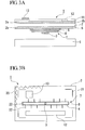
- Figs. 3A and 3B show the second embodiment of the invention.
- the second embodiment shares the basic structure with the first embodiment. Thus, only differences will be described herein.
- a number printed portion (optical identification portion) 12 is provided on a surface of the adhesive layer 5.
- An optically-readable optical identification ID (optical identification information) is written in the number printed portion 12.
- the number printed portion 12 includes characters or the like written by removing an ink-printed area through laser irradiation. Accordingly, the optical identification ID in the number printed portion 12 cannot be easily counterfeited.
- optical identification ID may include simple alphanumeric characters which can also be visually recognized.
- mechanical reading may include a one-dimensional bar code, a two-dimensional bar code, any image on which the identification ID is superimposed via an electronic watermark process, and array of dots and symbols.
- the optical identification ID can be related to the identification ID recorded on the IC chip 3 in the following manner.
- an optical identification ID is generated from the identification ID of the IC chip 3 by data conversion and the identification ID of the IC chip 3 is generated from the optical identification ID by data conversion.
- a function conversion including a cyclic redundancy check (CRC) and hash, symmetrical encryption, asymmetrical encryption, and the like may be employed.
- CRC cyclic redundancy check
- hash symmetrical encryption
- asymmetrical encryption asymmetrical encryption
- the optical identification ID is formed on the surface of the IC label 1 on which the security function layer (security function portion) 13 is provided. That is, the number printed portion 12 and the security function layer 13 are provided on the same surface of the label substrate 2 to prevent photocopying of the IC label 1.
- optical identification ID Forgery and counterfeit of the optical identification ID can be prevented by printing the optical identification ID in the upper part or the lower part of the security function layer 13, or laser-writing with ink entrained in the security function layer 13.
- Optical identification ID can be recorded on IC chip 3.
- the optical identification ID registered in the IC chip 3 can be taken out.
- Forgery of the IC label 1 can be prevented by comparing the optical identification ID taken out from the IC chip 3 with the optical identification ID printed on the IC label 1.
- the IC chip 3 may be used on which information including the identification ID cannot be re-written, and the identification ID may be a unique ID.
- the optical identification ID is associated on the database along with the information including the identification ID recorded on the IC chip 3.
- the information including the identification ID recorded on the IC chip 3 is read by the information reader, and the optical identification ID registered on the database is obtained based on the information including the identification ID.
- Forgery of the IC label 1 can be prevented by comparing the thus obtained optical identification ID on the database with the optical identification ID printed on the IC label 1.
- the information including the identification ID of the IC chip 3 cannot be forged, so prevention of forgery of the IC label 1 is highly effective.
- the IC chip 3 on which the information including the identification ID cannot be re-written may be used.
- the identification ID may be a unique ID.
- the optical identification ID generated from the information including the identification ID recorded on the memory using a function conversion including CRC and hash, symmetrical encryption and asymmetrical encryption, may be printed on the IC label 1.
- the information including the identification ID of the IC chip 3 is read by the information reader, and the data conversion, which is the same as in the generation of the optical identification ID, is carried out by the information reader to generate a comparative optical identification ID. Forgery of the IC label 1 can be prevented by comparing the generated comparative optical identification ID with the optical identification ID printed on the IC label 1.
- the optical identification IDs of both algorithms do not correspond with each other. That is, whether or not a proper data conversion algorithm exists in the information reader can also be confirmed, and authenticity of the information reader can also be verified.
- the information including the identification ID may be written in a non-rewritable memory by the manufacturer.
- the identification ID is a unique ID, forgery of the IC label 1 can be prevented in a simple manner on site without accessing the database.
- data conversion using a function conversion including hash, symmetrical encryption and asymmetrical encryption is conducted from the information including the identification ID recorded on memory to generate the optical identification ID.
- An arbitrary cryptographic key can be used for the data conversion.
- the optical identification ID printed on the IC label 1 and the comparative optical identification ID generated inside the information reader based on the information on the identification ID of the IC chip 3 correspond only when the following two conditions are satisfied.
- an operator may input the cryptographic key to the information reader and the cryptographic key may be managed to be known only by certain persons. Thus, both of authenticity of the information reader and authenticity of the operator (whether or not the operator has information on the cryptographic key) can be verified.
- the service identifier defines the bit length of the service ID.
- the service ID divides the identification IDs into groups and sets up the same ID for each group of customers, usage, intended purposes, managing purposes, and other groups of the identification IDs.
- the unique ID never overlaps with other IDs at least in the individual service identifier. That is, the sequence of the service ID and the unique ID have secured the inherent characteristic as the identification ID.
- An error detection code is generated during the data conversion from the identification ID except the EDC portion.
- the EDC aims at verifying authenticity of the identification ID. That is, when abnormalities occur in the identification ID due to malfunction of the reading operation of the identification ID, authenticity of the identification ID is verified through comparison of the EDC read out at the read-out of the identification ID with the EDC generated by the data conversion from the portion excluding the EDC from the read identification ID. If the read EDC and the EDC generated by the data conversion correspond with each other, it is determined that authenticity of the identification ID is verified. If they do not correspond with each other, it is determined that a read error has occurred or the identification ID is no longer valid, and the identification ID is not considered as authentic.
- the method of the data conversion to generate the EDC may include a function conversion including CRC and hash, symmetrical encryption and asymmetrical encryption.
- the header may be omitted.
- the header may be omitted if the service identifier is fixed information.
- the service ID may have a fixed length, or it may be omitted.
- the service ID may be omitted. If the service ID is omitted, the information showing that no service ID exists in the service identifier may be registered, or both of the service identifier and the service ID may be omitted. When no service ID exists, the inherent characteristic is secured as an identification ID using the unique ID.
- the EDC can be omitted when demand for authenticity of the identification ID is low.
- the group of customers, usage, intended purposes, managing purposes to which the identification ID belongs, and other groups of identification IDs can be distinguished by merely reading the identification ID.
- a specific service ID is used for the IC chip 3 of the IC label 1 used for the purpose, and the service ID is not used for other purposes.
- the service ID is not used for other purposes.
- Additional procedures may sometimes be required such as data conversion and sending of the identification ID to an information processor after reading the identification ID.
- a number of unnecessary processes can be omitted.
- reliability of the system can be improved.
- Authenticity of the label for forgery prevention can be verified in a simple manner by determining whether or not a predetermined service ID is contained in the read identification ID.
- authenticity of the label for forgery prevention can be verified in a simple manner by determining whether or not a predetermined service ID is contained in the read identification ID.
- authenticity of the IC label 1 can be verified in a simple manner even if one has no connection with the database. This is especially useful when the information reader is a handy, small and simple device which does not necessarily have connectivity to a database.
- a customer A affixes an IC label 1 with a service ID of "0001" to each of supplies for management of plural supplies stored in his/her office building B.
- An ID issuer using an ID issuing device refers to the customer A directly or indirectly, and assigns "0001" as a service ID only to the IC label 1 which the customer A affixed to the supply stored in the building B.
- the ID issuer does not issue an identification ID with a service ID of "0001" for other purposes.
- a customer C affixes an IC label 1 to each of notebook computers which staffs of his/her company carry out of the office.
- the ID issuer using the ID issuing device refers to the customer C directly or indirectly, and assigns "0010" as a service ID only to the IC label 1 which the customer C affixes to the notebook computer for carrying out of the office.
- the ID issuer does not issue an identification ID with a service ID of "0010" for other purposes.
- the customer A can immediately recognize that the article to which the IC label 1 is affixed is the article registered as a supply stored in the building B. Accordingly, authenticity can be verified in a simple manner.
- the identification ID is read by the information reader and the service ID is found to be "0010”
- the customer C can immediately recognize that the article to which the IC label 1 is affixed is the article registered in a notebook computer for carrying out of the office. Accordingly, authenticity can be verified in a simple manner.
- the customer A reads the identification ID, and only when he/she finds the service ID is "0001", sends the identification ID to the information processor and accesses the database for management of the supply stored in the office building B. Then, the customer A performs required data processing. Upon finding that the service ID is not "0001", the customer A does not execute these processes. Thus, unnecessary data processing is not required, and unnecessary processes can be omitted to improve system reliability.
- the customer B also obtains the same effect by executing data processing only when the service ID is "0010.”
- Figs. 4A to 4C show the third embodiment of the invention.
- the third embodiment shares the basic structure with the first embodiment. Thus, only differences will be described herein.
- a hook-shaped antenna slit 26 is formed in a longitudinal direction central portion of an antenna 4 for performing impedance matching between an IC chip 3 and the antenna 4.
- a stub 27 is formed by the antenna slit 26.
- the width of the antenna slit 26 is narrower than terminal intervals (interval of electrodes 30) of the IC chip 3.
- Power feeding portions 29 are provided to oppositely face each other with the antenna slit 26 disposed therebetween.
- the IC chip 3 is provided to straddle the antenna slit 26 so as to electrically connect the electrode 30 and the power feeding portions 29.
- the stub 27 formed by the antenna slit 26 is connected in series between the antenna 4 and the IC chip 3.
- the stub 27 works as an inductor component for antenna input impedance.
- capacitive component of the input impedance of the IC chip 3 can be offset and the antenna input impedance and the input impedance of the IC chip 3 can be matched. Appropriate setting of the impedance matching can transmit electric power generated at the antenna 4 efficiently to the IC chip 3.
- the impedance matching varies depending on the materials used in the IC label 1 or influence of a dielectric constant of the object to which IC label 1 is affixed.
- the impedance matching can be improved by changing the length of the antenna slit 26.
- an optimum design of the antenna slit 26 may sometimes be needed based on the materials required for the IC label 1, the materials of the object to which the IC label 1 is affixed, and the environment.
- the IC tag 7 may be provided to incline with respect to the label substrate 2.
- the IC label 1 may be affixed to straddle a mating surface 39 of a case 37 and a lid 38 as shown in Fig. 6 .
- the IC tag 7 is also disposed to straddle the mating surface 39.
- a common IC tag (non-contact IC medium) was used throughout the examples.
- An antenna was formed through etching an aluminum thin film formed on a 38 ⁇ m-thick PET film (base film). Cut-outs 23 as shown in Figs. 2 and 3B were formed in a circumference of the antenna at intervals of 4 mm. A feed terminal of the antenna and gold bumps of the IC chip were electrically connected and fixed using an anisotropic conductive adhesive agent to form an IC tag.
- Cut-outs were provided in the label substrate of art paper (60 mm in width, 39 mm in length, and 90 ⁇ m in thickness).
- the cut-outs were the same as those shown in Figs. 2 and 3B . That is, the cut-out 20 provided in outer circumference of the label substrate was formed in a continuous zigzag shape with length of 3 mm and width of 1.5 mm.
- the cut-out 21 formed at each corner of the label substrate was L-shaped with 7.5 mm-long slits running along the contour of the corner of the label substrate. The corner portion of the L shape remained uncut.
- the corner portion of the cut-out 21 was easily broken to leave a trace of removal of the label affixed to the object, which was easy to find.
- the cut-outs 22 were provided at an area where the antenna is placed to overlap the cut-outs 23 of the antenna at intervals of 4 mm.
- Ink with solvent color development property was applied to the surface (the first principal surface) of the label substrate to form a solvent color developing layer.
- a pattern was printed on the solvent color developing layer by offset printing to form a printed layer.
- a security function layer 13 was printed on the printed layer with fluorescent ink which becomes luminous when irradiated with ultraviolet light.
- An acrylic adhesive agent having adhesion of 30000 mN/25 mm was applied on the back surface (i.e., the second principal surface) of the label substrate.
- the non-contact IC medium (IC tag) was affixed to the adhesive agent to form an IC label A.
- a separator as a peel off sheet was temporarily attached to the adhesive agent.
- the separator (112 ⁇ m in thickness) formed by laminating polyethylene on one side of a sheet of kraft paper and then siliconized was temporarily attached to the adhesive agent as a peel off sheet.
- a solvent color developing layer, a printed layer and a security function layer 13 which becomes luminous when irradiated with ultraviolet light were formed on the first principal surface of the label substrate.
- the label substrate has slits as in the Example 1.
- a second security function layer 13 was formed on the security function layer 13 by printing with specific ink which becomes luminous when irradiated with infrared light with a wavelength of 780 nm.
- An acrylic adhesive agent with adhesion of 30000 mN/25 mm was applied to the second principal surface of the label substrate.
- a non-contact IC medium (IC tag) was attached to produce an IC label substrateparator (112 ⁇ m in thickness) which is the same as that in Example 1 was temporarily attached to the adhesive agent as a peel off sheet.
- a pattern was printed on the surface of a breakable film base to form a printed layer.
- An IC tag having no cut-outs 23 around the antenna was laminated on the back surface of the film base using the same non-contact IC medium as in Examples 1 and 2.
- the film base had cut-outs only in the circumference thereof.
- an IC label C was manufactured which had no cut-outs on the label surface and the IC tag portion in contrast with Examples, and had neither a solvent color developing layer nor a security function layer (the IC tag C only had a printed layer).
- a printed layer as formed by printing a pattern on one surface of the breakable film base and an IC tag was laminated on the back surface as in Comparative Example 1.
- An adhesive layer with adhesion of 5000 mN/25 mm was provided thereon to produce an IC label D.
- the label substrate and the antenna were broken at the same time from the four slits to completely destroy the function as a non-contact IC label.
- the solvent color developing layer developed color due to the solvent.
- a clear trace of removal was confirmed.
- a label substrate manufactured by color photocopying the label substrate from which the IC tag was removed and making cut-outs similar to those of authentic label substrate was confirmed as a forged label since it has no security function layer.
- the security function layer could be confirmed when irradiated with an infrared lamp. Thus, the IC label B was able to be distinguished from those forged or replicated.
- the label substrate could be broken when they were peeled off with great force due to slits and difference in adhesive strength.
- the IC labels C and D were not broken.
- the antenna was hard to break. It was possible to remove the IC labels C and D from the box 33 easily by using a solvent.
- the peeled IC labels C and D were able to be reused by affixing to another box.
- the IC labels were easily forged by color photocopying the pattern thereon.
Landscapes
- Engineering & Computer Science (AREA)
- Microelectronics & Electronic Packaging (AREA)
- Computer Hardware Design (AREA)
- Physics & Mathematics (AREA)
- General Physics & Mathematics (AREA)
- Theoretical Computer Science (AREA)
- Computer Security & Cryptography (AREA)
- General Engineering & Computer Science (AREA)
- Credit Cards Or The Like (AREA)
Claims (8)
- Etiquette à circuit intégré (1) pour la prévention de la contrefaçon, comprenant :un substrat d'étiquette (2) qui comporte un agent adhésif (5) permettant de fixer celui-ci à un objet ;un support de circuit intégré sans contact (7) qui est fourni sur le substrat d'étiquette (2) et comporte une puce de circuit intégré (3) permettant de stocker des informations d'identification prédéterminées et une antenne (4) pour la transmission sans fil des informations d'identification ; etune partie fonction de sécurité (13) qui est fournie sur le substrat d'étiquette (2),caractérisée en ce quele substrat d'étiquette (2) inclut au moins l'une parmi :une partie détection de solvant (15) qui est dissoute par un solvant de décollement pour décoller le substrat d'étiquette (2) fixé à l'objet, ou réagit chimiquement avec le solvant de décollement ; etune partie détection de chaleur (15) qui subit un changement de couleur lorsqu'elle est chauffée ou réagit chimiquement sous l'effet de la chaleur.
- Etiquette à circuit intégré (1) pour la prévention de la contrefaçon selon la revendication 1, dans laquelle le substrat d'étiquette (2) est formé d'un matériau cassable.
- Etiquette à circuit intégré (1) pour la prévention de la contrefaçon selon la revendication 1, dans laquelle les informations d'identification sont des informations d'identification intrinsèques à chaque puce de circuit intégré (3).
- Etiquette à circuit intégré (1) pour la prévention de la contrefaçon selon la revendication 1, dans laquelle les informations d'identification sont corrélées avec des informations de gestion pour la gestion de l'objet.
- Etiquette à circuit intégré (1) pour la prévention de la contrefaçon selon la revendication 1, dans laquelle :la puce de circuit intégré (3) inclut une mémoire morte ; etles informations d'identification sont stockées dans la mémoire morte.
- Etiquette à circuit intégré (1) pour la prévention de la contrefaçon selon la revendication 1, dans laquelle la partie fonction de sécurité (13) inclut au moins l'un parmi :un matériau fonctionnel à témoin optique qui subit un changement de couleur en fonction d'un angle d'une lumière venant frapper la partie fonction de sécurité (13) ou d'un angle de reconnaissance visuelle de la partie fonction de sécurité (13) ;un matériau fluorescent ou un matériau phosphorescent excité par des ondes électromagnétiques d'une longueur d'onde spécifiée pour émettre des ondes électromagnétiques d'une longueur d'onde différente de celle de la longueur d'onde spécifiée ; etun matériau de cristal liquide qui a une polarisabilité d'un diagramme spécifique et affiche le diagramme en enlevant la lumière spécifiquement polarisée.
- Etiquette à circuit intégré (1) pour la prévention de la contrefaçon selon la revendication 1, dans laquelle :le substrat d'étiquette (2) inclut une partie identification optique (12) qui comporte des informations d'identification optiques lisibles optiquement ; etles informations d'identification et les informations d'identification optiques sont corrélées au moins partiellement entre elles.
- Etiquette à circuit intégré (1) pour la prévention de la contrefaçon selon la revendication 7, dans laquelle la partie fonction de sécurité (13) et la partie identification optique (12) sont fournies sur la même surface du substrat d'étiquette (2).
Applications Claiming Priority (2)
| Application Number | Priority Date | Filing Date | Title |
|---|---|---|---|
| JP2006136284 | 2006-05-16 | ||
| PCT/JP2007/060066 WO2007132897A1 (fr) | 2006-05-16 | 2007-05-16 | Étiquette de circuit intégré pour prévenir la contrefaçon |
Publications (3)
| Publication Number | Publication Date |
|---|---|
| EP2020654A1 EP2020654A1 (fr) | 2009-02-04 |
| EP2020654A4 EP2020654A4 (fr) | 2016-07-27 |
| EP2020654B1 true EP2020654B1 (fr) | 2019-10-16 |
Family
ID=38693986
Family Applications (1)
| Application Number | Title | Priority Date | Filing Date |
|---|---|---|---|
| EP07743501.4A Ceased EP2020654B1 (fr) | 2006-05-16 | 2007-05-16 | Étiquette de circuit intégré pour prévenir la contrefaçon |
Country Status (7)
| Country | Link |
|---|---|
| US (1) | US8395504B2 (fr) |
| EP (1) | EP2020654B1 (fr) |
| JP (2) | JPWO2007132897A1 (fr) |
| KR (1) | KR20090024675A (fr) |
| CN (1) | CN101443832B (fr) |
| TW (1) | TWI478068B (fr) |
| WO (1) | WO2007132897A1 (fr) |
Families Citing this family (55)
| Publication number | Priority date | Publication date | Assignee | Title |
|---|---|---|---|---|
| US7162035B1 (en) | 2000-05-24 | 2007-01-09 | Tracer Detection Technology Corp. | Authentication method and system |
| US7380131B1 (en) | 2001-01-19 | 2008-05-27 | Xilinx, Inc. | Copy protection without non-volatile memory |
| US8171567B1 (en) | 2002-09-04 | 2012-05-01 | Tracer Detection Technology Corp. | Authentication method and system |
| EP2020654B1 (fr) * | 2006-05-16 | 2019-10-16 | Toppan Printing Co., Ltd. | Étiquette de circuit intégré pour prévenir la contrefaçon |
| US10870740B2 (en) | 2007-08-12 | 2020-12-22 | Toyota Jidosha Kabushiki Kaisha | Non-color shifting multilayer structures and protective coatings thereon |
| US8861087B2 (en) | 2007-08-12 | 2014-10-14 | Toyota Motor Corporation | Multi-layer photonic structures having omni-directional reflectivity and coatings incorporating the same |
| US9739917B2 (en) | 2007-08-12 | 2017-08-22 | Toyota Motor Engineering & Manufacturing North America, Inc. | Red omnidirectional structural color made from metal and dielectric layers |
| US10690823B2 (en) | 2007-08-12 | 2020-06-23 | Toyota Motor Corporation | Omnidirectional structural color made from metal and dielectric layers |
| US10788608B2 (en) | 2007-08-12 | 2020-09-29 | Toyota Jidosha Kabushiki Kaisha | Non-color shifting multilayer structures |
| US8329247B2 (en) | 2009-02-19 | 2012-12-11 | Toyota Motor Engineering & Manufacturing North America, Inc. | Methods for producing omni-directional multi-layer photonic structures |
| US10048415B2 (en) | 2007-08-12 | 2018-08-14 | Toyota Motor Engineering & Manufacturing North America, Inc. | Non-dichroic omnidirectional structural color |
| US8593728B2 (en) * | 2009-02-19 | 2013-11-26 | Toyota Motor Engineering & Manufacturing North America, Inc. | Multilayer photonic structures |
| US9612369B2 (en) | 2007-08-12 | 2017-04-04 | Toyota Motor Engineering & Manufacturing North America, Inc. | Red omnidirectional structural color made from metal and dielectric layers |
| JP2009134528A (ja) * | 2007-11-30 | 2009-06-18 | Toppan Printing Co Ltd | 偽造防止用icラベル |
| JP5236939B2 (ja) * | 2007-12-21 | 2013-07-17 | 大日本印刷株式会社 | データキャリア |
| JP5167828B2 (ja) * | 2008-01-21 | 2013-03-21 | 凸版印刷株式会社 | 偽造防止用icタグ |
| JP5194861B2 (ja) * | 2008-02-12 | 2013-05-08 | 凸版印刷株式会社 | 非接触icラベル |
| JP2009250817A (ja) * | 2008-04-08 | 2009-10-29 | Univ Of Yamanashi | 偽造品検出方法、偽造品検出に用いられる識別タグ、偽造品検出装置、識別タグを備えるインクカートリッジ、および偽造品検出装置を用いる印刷装置 |
| US7995196B1 (en) | 2008-04-23 | 2011-08-09 | Tracer Detection Technology Corp. | Authentication method and system |
| JP5311022B2 (ja) * | 2009-01-08 | 2013-10-09 | 凸版印刷株式会社 | Icタグインレット付き光学可変デバイス |
| JP2010231681A (ja) * | 2009-03-30 | 2010-10-14 | Hitachi Ltd | Rfidタグラベル及びその使用方法 |
| DE102009036706C5 (de) * | 2009-08-08 | 2017-04-13 | Friedrich Kisters | Sicherheitselement mit einer elektronischen Anzeigevorrichtung zur Darstellung von sicherheitsrelevanten Informationen oder Mustern, seine Verwendung als Bestandteil einer elektronischen Telekommunikationseinrichtung sowie ein Verfahren zur Kennzeichnung, Identifikation oder Authentifikation von Gegenständen oder Lebewesen |
| JP5803059B2 (ja) * | 2010-03-31 | 2015-11-04 | 凸版印刷株式会社 | 貼り換え防止機能付き偽造防止封印ラベル |
| JP5464028B2 (ja) * | 2010-04-19 | 2014-04-09 | 凸版印刷株式会社 | 偽変造防止用icラベル |
| JP2011243135A (ja) * | 2010-05-21 | 2011-12-01 | Sony Corp | 情報処理装置および方法、並びにプログラム |
| US8257784B2 (en) | 2010-08-10 | 2012-09-04 | Toyota Motor Engineering & Manufacturing North America, Inc. | Methods for identifying articles of manufacture |
| US8196823B2 (en) | 2010-08-10 | 2012-06-12 | Toyota Motor Engineering & Manufacturing North America, Inc. | Optical lock systems and methods |
| US10067265B2 (en) | 2010-10-12 | 2018-09-04 | Toyota Motor Engineering & Manufacturing North America, Inc. | Semi-transparent reflectors |
| US8908968B1 (en) * | 2010-10-28 | 2014-12-09 | Movie Poster Grading and Registry Company, LLC | Identifying and ensuring the authenticity of objects |
| EP2455825B1 (fr) * | 2010-11-18 | 2016-08-17 | Nivarox-FAR S.A. | Procédé d'appairage et d'ajustement d'un sous-ensemble d'horlogerie |
| US8427193B1 (en) | 2010-12-07 | 2013-04-23 | Xilinx, Inc. | Intellectual property core protection for integrated circuits |
| US8418006B1 (en) | 2010-12-07 | 2013-04-09 | Xilinx, Inc. | Protecting a design for an integrated circuit using a unique identifier |
| US8386990B1 (en) * | 2010-12-07 | 2013-02-26 | Xilinx, Inc. | Unique identifier derived from an intrinsic characteristic of an integrated circuit |
| JP2012250505A (ja) * | 2011-06-06 | 2012-12-20 | Fujifilm Corp | 複屈折性転写箔 |
| FR2985985B1 (fr) | 2012-01-23 | 2014-02-21 | Emmanuel Thibaudeau | Scelle inviolable pour emballage, procede de fabrication et utilisation d'un scelle inviolable |
| WO2013116525A1 (fr) * | 2012-01-31 | 2013-08-08 | Checkpoint Systems, Inc. | Dispositif de sécurité à bande flexible |
| CN103577859A (zh) * | 2012-08-03 | 2014-02-12 | 天津阿波罗电子有限公司 | 一种新型手机识别代码系统的构成方法 |
| US9664832B2 (en) | 2012-08-10 | 2017-05-30 | Toyota Motor Engineering & Manufacturing North America, Inc. | Omnidirectional high chroma red structural color with combination semiconductor absorber and dielectric absorber layers |
| US9678260B2 (en) | 2012-08-10 | 2017-06-13 | Toyota Motor Engineering & Manufacturing North America, Inc. | Omnidirectional high chroma red structural color with semiconductor absorber layer |
| US9658375B2 (en) | 2012-08-10 | 2017-05-23 | Toyota Motor Engineering & Manufacturing North America, Inc. | Omnidirectional high chroma red structural color with combination metal absorber and dielectric absorber layers |
| CN103971590B (zh) * | 2013-02-01 | 2017-02-22 | 比亚迪股份有限公司 | 一种防伪商标及其制造方法 |
| US9626620B2 (en) * | 2013-06-05 | 2017-04-18 | Haemonetics Corporation | Frangible RFID tag and method of producing same |
| JP2015069499A (ja) * | 2013-09-30 | 2015-04-13 | 凸版印刷株式会社 | 脆性機能を有する非接触型情報媒体 |
| JP6741586B2 (ja) | 2014-04-01 | 2020-08-19 | トヨタ モーター エンジニアリング アンド マニュファクチャリング ノース アメリカ,インコーポレイティド | 色シフトのない多層構造 |
| EP3146475B1 (fr) | 2014-05-23 | 2022-11-16 | Avery Dennison Retail Information Services LLC | Marqueurs pour marchandises incorporant une antenne durable |
| WO2016002316A1 (fr) * | 2014-06-30 | 2016-01-07 | リンテック株式会社 | Feuille adhésive et son procédé de production |
| US9810824B2 (en) | 2015-01-28 | 2017-11-07 | Toyota Motor Engineering & Manufacturing North America, Inc. | Omnidirectional high chroma red structural colors |
| EP3346245A4 (fr) * | 2015-09-03 | 2019-06-05 | Hitachi, Ltd. | Indicateur d'historique des températures |
| US11038278B2 (en) * | 2019-08-15 | 2021-06-15 | United States Of America As Represented By The Secretary Of The Navy | Lens apparatus and methods for an antenna |
| KR102099045B1 (ko) * | 2019-08-16 | 2020-04-08 | 장유성 | 부분접착라벨 스티커 |
| US20230146326A1 (en) * | 2020-02-26 | 2023-05-11 | Avery Dennison Retail Information Services Llc | Rfid security label for packaging |
| JP7497631B2 (ja) * | 2020-07-08 | 2024-06-11 | Toppanホールディングス株式会社 | 貼り替え防止用ラベルおよびその読み取り判定方法 |
| CN117882084A (zh) * | 2021-08-30 | 2024-04-12 | 普利司通美国轮胎运营有限责任公司 | 用于轮胎的rfid封装 |
| US20240331513A1 (en) * | 2023-02-21 | 2024-10-03 | Steven Halliwell | Tamper-resistant security for artworks and collectibles |
| CN117612445A (zh) * | 2023-10-07 | 2024-02-27 | 中国印钞造币集团有限公司 | 防伪元件及其制备方法和防伪物品 |
Family Cites Families (18)
| Publication number | Priority date | Publication date | Assignee | Title |
|---|---|---|---|---|
| JPH10250228A (ja) | 1997-03-13 | 1998-09-22 | Mitsubishi Paper Mills Ltd | 偽造防止シート及び偽造防止粘着ラベル |
| US7061831B2 (en) * | 1997-03-28 | 2006-06-13 | Carlos De La Huerga | Product labeling method and apparatus |
| JP3830232B2 (ja) * | 1997-06-16 | 2006-10-04 | リンテック株式会社 | 封印シール |
| JP2001013874A (ja) | 1999-06-25 | 2001-01-19 | Matsushita Electric Works Ltd | Idラベル |
| JP2002211756A (ja) * | 2001-01-16 | 2002-07-31 | Toppan Forms Co Ltd | 配送伝票 |
| JP2003029637A (ja) * | 2001-07-12 | 2003-01-31 | Toppan Printing Co Ltd | 封印シール |
| JP3854124B2 (ja) | 2001-11-08 | 2006-12-06 | 日立化成工業株式会社 | 非接触式icラベル |
| JP2004258089A (ja) * | 2003-02-24 | 2004-09-16 | Dainippon Ink & Chem Inc | 感熱記録層を有する再使用防止ラベル |
| US6975765B2 (en) * | 2003-05-06 | 2005-12-13 | New Light Industries, Ltd. | Optically variable form birefringent structure and method and system and method for reading same |
| ATE530998T1 (de) * | 2003-07-07 | 2011-11-15 | Avery Dennison Corp | Rfid-einrichtung mit änderbaren charakteristika |
| JP2005216054A (ja) | 2004-01-30 | 2005-08-11 | Toppan Label Co Ltd | 貼り換え防止用icラベル |
| JP2005309935A (ja) * | 2004-04-23 | 2005-11-04 | Toppan Label Co Ltd | 貼り換え防止用icラベル |
| TWI268258B (en) * | 2004-09-06 | 2006-12-11 | Ind Tech Res Inst | Package container cover with counterfeit identification functions with antenna functions for transmitting product identification information and detachment destruction functions for preventing re-use of identification chip |
| JP4402574B2 (ja) | 2004-11-15 | 2010-01-20 | 花王株式会社 | ムタナーゼ |
| FI121831B (fi) * | 2005-07-07 | 2011-04-29 | M Real Oyj | Anturirakenne, menetelmä sen valmistamiseksi ja siitä valmistettava tuote |
| US7598868B2 (en) * | 2005-09-21 | 2009-10-06 | The Boeing Company | Methods and systems for monitoring components using radio frequency identification |
| EP2020654B1 (fr) * | 2006-05-16 | 2019-10-16 | Toppan Printing Co., Ltd. | Étiquette de circuit intégré pour prévenir la contrefaçon |
| FR2929738B1 (fr) * | 2008-04-04 | 2011-01-28 | Arjowiggins Licensing Sas | Document comportant un dispositif a microcircuit integre et procede de detection de l'atteinte a l'integrite physique du document |
-
2007
- 2007-05-16 EP EP07743501.4A patent/EP2020654B1/fr not_active Ceased
- 2007-05-16 KR KR1020087027588A patent/KR20090024675A/ko not_active Ceased
- 2007-05-16 TW TW096117502A patent/TWI478068B/zh not_active IP Right Cessation
- 2007-05-16 US US12/227,285 patent/US8395504B2/en not_active Expired - Fee Related
- 2007-05-16 WO PCT/JP2007/060066 patent/WO2007132897A1/fr not_active Ceased
- 2007-05-16 JP JP2008515593A patent/JPWO2007132897A1/ja active Pending
- 2007-05-16 CN CN2007800172044A patent/CN101443832B/zh not_active Expired - Fee Related
-
2012
- 2012-10-24 JP JP2012235084A patent/JP2013029865A/ja active Pending
Non-Patent Citations (1)
| Title |
|---|
| None * |
Also Published As
| Publication number | Publication date |
|---|---|
| JPWO2007132897A1 (ja) | 2009-09-24 |
| WO2007132897A1 (fr) | 2007-11-22 |
| TWI478068B (zh) | 2015-03-21 |
| CN101443832A (zh) | 2009-05-27 |
| JP2013029865A (ja) | 2013-02-07 |
| CN101443832B (zh) | 2011-03-02 |
| TW200813852A (en) | 2008-03-16 |
| US20090303044A1 (en) | 2009-12-10 |
| EP2020654A4 (fr) | 2016-07-27 |
| EP2020654A1 (fr) | 2009-02-04 |
| KR20090024675A (ko) | 2009-03-09 |
| US8395504B2 (en) | 2013-03-12 |
Similar Documents
| Publication | Publication Date | Title |
|---|---|---|
| EP2020654B1 (fr) | Étiquette de circuit intégré pour prévenir la contrefaçon | |
| JP5012046B2 (ja) | 偽造防止用icラベル | |
| JP5464028B2 (ja) | 偽変造防止用icラベル | |
| US7872579B2 (en) | Structure including an electronic device, in particular for fabricating a security document or a document of value | |
| US20110215909A1 (en) | Structure including at least two integrated microcircuit devices with contactless communication | |
| JP2009075712A (ja) | 偽造防止用icラベル | |
| AU2010214781A1 (en) | A radio frequency identification tag with tamper detection capability | |
| JP4835448B2 (ja) | 偽造防止用icラベル | |
| US8079519B2 (en) | Structure including an electronic device for making a security document | |
| EP1810266A1 (fr) | Procede et dispositif de verification de non intrusion dans un systeme et / ou de non atteinte a l'integrite d'un objet ou de son contenu | |
| JP2009134528A (ja) | 偽造防止用icラベル | |
| JP2009075711A (ja) | 偽造防止用icラベル | |
| US11305514B2 (en) | Laminate, verification, and method of producing laminate | |
| CN102640169A (zh) | 用于制造包括电子装置的支承件的方法 | |
| JP4048788B2 (ja) | カード | |
| JP2014134997A (ja) | フィルムアンテナとその製造方法並びにrfidラベル | |
| JP2011112758A (ja) | 非接触icラベルおよび貼付体 | |
| JP2011238044A (ja) | 偽造防止icラベル | |
| JP4529486B2 (ja) | 非接触ic媒体 | |
| JP2010019913A (ja) | 剥離及び開封防止媒体 | |
| JP2016081015A (ja) | 封印シール | |
| JP2011150409A (ja) | セキュリティ文書 | |
| JP2011227544A (ja) | 券種判別システム及び券種判別方法 | |
| KR20150076370A (ko) | 홀로그램 칩리스 rfid 태그 및 그의 제조 방법 | |
| JP2009217777A (ja) | Rfidタグ |
Legal Events
| Date | Code | Title | Description |
|---|---|---|---|
| PUAI | Public reference made under article 153(3) epc to a published international application that has entered the european phase |
Free format text: ORIGINAL CODE: 0009012 |
|
| 17P | Request for examination filed |
Effective date: 20081126 |
|
| AK | Designated contracting states |
Kind code of ref document: A1 Designated state(s): AT BE BG CH CY CZ DE DK EE ES FI FR GB GR HU IE IS IT LI LT LU LV MC MT NL PL PT RO SE SI SK TR |
|
| AX | Request for extension of the european patent |
Extension state: AL BA HR MK RS |
|
| DAX | Request for extension of the european patent (deleted) | ||
| RBV | Designated contracting states (corrected) |
Designated state(s): DE FR GB |
|
| RAP1 | Party data changed (applicant data changed or rights of an application transferred) |
Owner name: TOPPAN PRINTING CO., LTD. |
|
| RA4 | Supplementary search report drawn up and despatched (corrected) |
Effective date: 20160624 |
|
| RIC1 | Information provided on ipc code assigned before grant |
Ipc: G06K 19/07 20060101ALI20160620BHEP Ipc: G06K 19/073 20060101ALI20160620BHEP Ipc: G09F 3/00 20060101AFI20160620BHEP Ipc: G06K 19/077 20060101ALI20160620BHEP Ipc: G06K 19/10 20060101ALI20160620BHEP Ipc: G09F 3/02 20060101ALI20160620BHEP |
|
| GRAP | Despatch of communication of intention to grant a patent |
Free format text: ORIGINAL CODE: EPIDOSNIGR1 |
|
| INTG | Intention to grant announced |
Effective date: 20190429 |
|
| GRAS | Grant fee paid |
Free format text: ORIGINAL CODE: EPIDOSNIGR3 |
|
| GRAA | (expected) grant |
Free format text: ORIGINAL CODE: 0009210 |
|
| AK | Designated contracting states |
Kind code of ref document: B1 Designated state(s): DE FR GB |
|
| REG | Reference to a national code |
Ref country code: GB Ref legal event code: FG4D |
|
| REG | Reference to a national code |
Ref country code: DE Ref legal event code: R096 Ref document number: 602007059366 Country of ref document: DE |
|
| REG | Reference to a national code |
Ref country code: DE Ref legal event code: R097 Ref document number: 602007059366 Country of ref document: DE |
|
| PLBE | No opposition filed within time limit |
Free format text: ORIGINAL CODE: 0009261 |
|
| STAA | Information on the status of an ep patent application or granted ep patent |
Free format text: STATUS: NO OPPOSITION FILED WITHIN TIME LIMIT |
|
| 26N | No opposition filed |
Effective date: 20200717 |
|
| PGFP | Annual fee paid to national office [announced via postgrant information from national office to epo] |
Ref country code: DE Payment date: 20210420 Year of fee payment: 15 Ref country code: FR Payment date: 20210412 Year of fee payment: 15 |
|
| PGFP | Annual fee paid to national office [announced via postgrant information from national office to epo] |
Ref country code: GB Payment date: 20210422 Year of fee payment: 15 |
|
| REG | Reference to a national code |
Ref country code: DE Ref legal event code: R119 Ref document number: 602007059366 Country of ref document: DE |
|
| GBPC | Gb: european patent ceased through non-payment of renewal fee |
Effective date: 20220516 |
|
| PG25 | Lapsed in a contracting state [announced via postgrant information from national office to epo] |
Ref country code: FR Free format text: LAPSE BECAUSE OF NON-PAYMENT OF DUE FEES Effective date: 20220531 |
|
| PG25 | Lapsed in a contracting state [announced via postgrant information from national office to epo] |
Ref country code: GB Free format text: LAPSE BECAUSE OF NON-PAYMENT OF DUE FEES Effective date: 20220516 Ref country code: DE Free format text: LAPSE BECAUSE OF NON-PAYMENT OF DUE FEES Effective date: 20221201 |