EP2020692A1 - Dispositif de film piézo-électrique - Google Patents
Dispositif de film piézo-électrique Download PDFInfo
- Publication number
- EP2020692A1 EP2020692A1 EP07742718A EP07742718A EP2020692A1 EP 2020692 A1 EP2020692 A1 EP 2020692A1 EP 07742718 A EP07742718 A EP 07742718A EP 07742718 A EP07742718 A EP 07742718A EP 2020692 A1 EP2020692 A1 EP 2020692A1
- Authority
- EP
- European Patent Office
- Prior art keywords
- piezoelectric
- electrostrictive film
- thin
- electrode
- walled diaphragm
- Prior art date
- Legal status (The legal status is an assumption and is not a legal conclusion. Google has not performed a legal analysis and makes no representation as to the accuracy of the status listed.)
- Granted
Links
Images


Classifications
-
- H—ELECTRICITY
- H10—SEMICONDUCTOR DEVICES; ELECTRIC SOLID-STATE DEVICES NOT OTHERWISE PROVIDED FOR
- H10N—ELECTRIC SOLID-STATE DEVICES NOT OTHERWISE PROVIDED FOR
- H10N30/00—Piezoelectric or electrostrictive devices
- H10N30/80—Constructional details
- H10N30/87—Electrodes or interconnections, e.g. leads or terminals
- H10N30/875—Further connection or lead arrangements, e.g. flexible wiring boards, terminal pins
-
- G—PHYSICS
- G01—MEASURING; TESTING
- G01N—INVESTIGATING OR ANALYSING MATERIALS BY DETERMINING THEIR CHEMICAL OR PHYSICAL PROPERTIES
- G01N29/00—Investigating or analysing materials by the use of ultrasonic, sonic or infrasonic waves; Visualisation of the interior of objects by transmitting ultrasonic or sonic waves through the object
- G01N29/02—Analysing fluids
- G01N29/022—Fluid sensors based on microsensors, e.g. quartz crystal-microbalance [QCM], surface acoustic wave [SAW] devices, tuning forks, cantilevers, flexural plate wave [FPW] devices
-
- G—PHYSICS
- G01—MEASURING; TESTING
- G01N—INVESTIGATING OR ANALYSING MATERIALS BY DETERMINING THEIR CHEMICAL OR PHYSICAL PROPERTIES
- G01N29/00—Investigating or analysing materials by the use of ultrasonic, sonic or infrasonic waves; Visualisation of the interior of objects by transmitting ultrasonic or sonic waves through the object
- G01N29/22—Details, e.g. general constructional or apparatus details
- G01N29/24—Probes
- G01N29/2437—Piezoelectric probes
- G01N29/245—Ceramic probes, e.g. lead zirconate titanate [PZT] probes
-
- G—PHYSICS
- G01—MEASURING; TESTING
- G01P—MEASURING LINEAR OR ANGULAR SPEED, ACCELERATION, DECELERATION, OR SHOCK; INDICATING PRESENCE, ABSENCE, OR DIRECTION, OF MOVEMENT
- G01P15/00—Measuring acceleration; Measuring deceleration; Measuring shock, i.e. sudden change of acceleration
- G01P15/02—Measuring acceleration; Measuring deceleration; Measuring shock, i.e. sudden change of acceleration by making use of inertia forces using solid seismic masses
- G01P15/08—Measuring acceleration; Measuring deceleration; Measuring shock, i.e. sudden change of acceleration by making use of inertia forces using solid seismic masses with conversion into electric or magnetic values
- G01P15/09—Measuring acceleration; Measuring deceleration; Measuring shock, i.e. sudden change of acceleration by making use of inertia forces using solid seismic masses with conversion into electric or magnetic values by piezoelectric pick-up
- G01P15/0922—Measuring acceleration; Measuring deceleration; Measuring shock, i.e. sudden change of acceleration by making use of inertia forces using solid seismic masses with conversion into electric or magnetic values by piezoelectric pick-up of the bending or flexing mode type
-
- H—ELECTRICITY
- H10—SEMICONDUCTOR DEVICES; ELECTRIC SOLID-STATE DEVICES NOT OTHERWISE PROVIDED FOR
- H10N—ELECTRIC SOLID-STATE DEVICES NOT OTHERWISE PROVIDED FOR
- H10N30/00—Piezoelectric or electrostrictive devices
- H10N30/20—Piezoelectric or electrostrictive devices with electrical input and mechanical output, e.g. functioning as actuators or vibrators
- H10N30/204—Piezoelectric or electrostrictive devices with electrical input and mechanical output, e.g. functioning as actuators or vibrators using bending displacement, e.g. unimorph, bimorph or multimorph cantilever or membrane benders
- H10N30/2047—Membrane type
-
- H—ELECTRICITY
- H10—SEMICONDUCTOR DEVICES; ELECTRIC SOLID-STATE DEVICES NOT OTHERWISE PROVIDED FOR
- H10N—ELECTRIC SOLID-STATE DEVICES NOT OTHERWISE PROVIDED FOR
- H10N30/00—Piezoelectric or electrostrictive devices
- H10N30/30—Piezoelectric or electrostrictive devices with mechanical input and electrical output, e.g. functioning as generators or sensors
- H10N30/302—Sensors
Definitions
- the present invention relates to a piezoelectric/electrostrictive film element which utilizes vibration characteristics of its thin-walled diaphragm portion.
- piezoelectric/electrostrictive film elements of this kind include actuators which utilize flexural displacements of their thin-walled diaphragm portions, and sensors (e.g., microphones and viscosity sensors) for detecting characteristics (e.g., fluidal characteristic, sound pressure, very small weight, and acceleration) of media in the proximity of the thin-walled diaphragm portions.
- sensors e.g., microphones and viscosity sensors
- Patent Document 1 Japanese Patent Application Laid-Open ( kokai ) Nos. H8-201265 (Patent Document 1), 2002-261347 (Patent Document 2), and 2005-322890 (Patent Document 3) disclose piezoelectric/electrostrictive film elements which serve as the above-mentioned sensors.
- the piezoelectric/electrostrictive film sensors are configured to be able to utilize the correlation between the amplitude of a piezoelectric/electrostrictive film vibrator and the viscous resistance of fluid in contact with the vibrator and to measure characteristics, such as density, concentration, and viscosity, of the fluid.
- the vibrator when the vibrator is vibrated in the presence of the fluid, the vibrator is subjected to a dynamic resistance caused by viscosity of the fluid. In the meantime, a mechanical vibrating condition of the vibrator can be replaced with an equivalent electrical circuit. Accordingly, on the basis of viscous resistance to which the vibrator is subjected, an electrical constant of an equivalent circuit of a piezoelectric/electrostrictive film serving as the vibrator varies. By detecting variation of the electrical constant, characteristics, such as viscosity, density, and concentration, of the fluid can be measured.
- Fluid whose characteristics can be measured by such the piezoelectric/electrostrictive film sensors encompasses liquid and gas.
- liquid serving as an object of measurement include, as a matter of course, a single-component liquid formed solely of a main medium selected from among, for example, water, alcohol, oil, etc.
- the examples of the object-of-measurement liquid can include a liquid substance (slurry, paste, or the like) formed in such a manner that another medium that is soluble, lightly soluble, or insoluble in such a main medium is added to (dissolved in, mixed with, diffused in, or suspended in) the main medium.
- examples of the above-mentioned electrical constant include loss factor, phase, resistance, reactance, conductance, susceptance, inductance, and capacitance.
- phase, or loss factor which has a single maximal or minimal variation point in the vicinity of the resonance frequency of an equivalent circuit, is preferably used. This enables measurement of density and concentration of the fluid in addition to viscosity of the fluid. For example, the concentration of sulfuric acid in an aqueous solution of sulfuric acid can be measured.
- variation of resonance frequency can be used as an index for detecting variation in vibrating condition, so long as no particular problem arises in terms of accuracy of measurement, and durability.
- This kind of piezoelectric/electrostrictive film element has conventionally had problems with durability. For example, an attempt to improve element characteristics (sensor sensitivity, etc.) through increase in flexural displacement and internal stress of the aforementioned thin-walled diaphragm portion has been accompanied by occurrence of cracking in the aforementioned piezoelectric/electrostrictive film.
- an object of the present invention is to provide a piezoelectric/electrostrictive film element having excellent element characteristics and durability.
- a piezoelectric/electrostrictive film element of the present invention comprises a substrate, a lower electrode, a piezoelectric/electrostrictive film, and an upper electrode.
- the substrate has a thin-walled diaphragm portion, and a thick portion formed around the thin-walled diaphragm portion.
- the lower electrode is formed on the substrate in such a manner as to extend over the thin-walled diaphragm portion and the thick portion.
- the piezoelectric/electrostrictive film is formed on the lower electrode.
- the upper electrode is provided on the piezoelectric/electrostrictive film in such a manner as to face the thin-walled diaphragm portion.
- the present invention is characterized in that, in the piezoelectric/electrostrictive film element comprising the substrate, the lower electrode, the piezoelectric/electrostrictive film, and the upper electrode, the upper electrode comprises an upper-electrode body portion having a planar shape generally similar to a planar shape of the thin-walled diaphragm portion, and a connection portion provided continuously with the upper-electrode body portion.
- the upper-electrode body portion is provided in such a manner as to face the thin-walled diaphragm portion.
- the connection portion has a width narrower than that of the upper-electrode body portion.
- the thin-walled diaphragm portion corresponding to the upper-electrode body portion vibrates.
- a predetermined output is generated between the upper-electrode body portion and the lower electrode.
- the planar shape of the upper-electrode body portion is generally similar to that of the thin-walled diaphragm portion.
- the thin-walled diaphragm portion on the basis of the input voltage, can be more efficiently set in a predetermined vibrating condition.
- a vibrating condition of the thin-walled diaphragm portion can be more efficiently reflected in the output. This enables obtainment of a high output without need to increase an input voltage. Therefore, according to the present invention, the occurrence of cracking in the piezoelectric/electrostrictive film can be restrained, and thus durability can be improved, whereby a more excellent piezoelectric/electrostrictive film element is obtained.
- the piezoelectric/electrostrictive film element of the present invention may further comprise an auxiliary electrode.
- the auxiliary electrode is formed on the substrate in such a manner as to extend over the thick portion and an end portion of the thin-walled diaphragm portion and to be separated from the lower electrode. Further, the auxiliary electrode is connected to the connection portion.
- the piezoelectric/electrostrictive film element is configured as follows.
- the lower electrode is formed on the substrate in a region ranging from the thick portion adjacent to a first end of the thin-walled diaphragm portion to a position located toward the first end from an opposite second end of the thin-walled diaphragm portion.
- the auxiliary electrode is formed on the substrate in a region ranging from the thick portion adjacent to the second end of the thin-walled diaphragm portion to a position located toward the first end from the second end, in such a manner as to be separated from the lower electrode. That is, the lower electrode and the auxiliary electrode are formed on substantially the same plane while being separated from each other by a predetermined gap. The gap is formed at a position located toward the first end from the second end of the thin-walled diaphragm portion; in other words, on the thin-walled diaphragm portion.
- the piezoelectric/electrostrictive film is formed on the lower electrode and the auxiliary electrode in such a manner that an end portion of the lower electrode and an end portion of the auxiliary electrode are exposed on the thick portion.
- the upper-electrode body portion is provided in such a manner as to face the thin-walled diaphragm portion with the lower electrode and the piezoelectric/electrostrictive film intervening therebetween.
- the connection portion is provided on the piezoelectric/electrostrictive film and the auxiliary electrode so as to connect the upper-electrode body portion and the auxiliary electrode.
- flexural stress is maximized at connections between the thin-walled diaphragm portion and the thick portion; i.e., at the first and second ends of the thin-walled diaphragm portion.
- a defect such as a notch or a very small crack in the form of material discontinuity
- stress concentrates at the defect.
- a fatigue crack starts from the defect and is developed in the piezoelectric/electrostrictive film.
- the gap is not formed at positions corresponding to the first and second ends of the thin-walled diaphragm portion.
- the above-mentioned configuration can effectively restrain the generation of crack starting from the gap in the piezoelectric/electrostrictive film.
- the piezoelectric/electrostrictive film in a region which is located in the vicinity of the second end of the thin-walled diaphragm portion and which extends over the thin-walled diaphragm portion and the thick portion, the piezoelectric/electrostrictive film is provided between the auxiliary electrode and the upper electrode, which have the same electric potential. That is, in the region in the vicinity of the second end of the thin-walled diaphragm portion, the piezoelectric/electrostrictive film has a portion (inactive portion) to which an electric field is not applied.
- a portion of the piezoelectric/electrostrictive film which, upon application of the electric field thereto, causes the thin-walled diaphragm portion to flexurally deform is located toward the "inside" of the thin-walled diaphragm portion from the second end.
- the thin-walled diaphragm portion can be efficiently excited.
- an output is efficiently generated from between the upper electrode and the lower electrode according to a vibrating condition of the thin-walled diaphragm portion.
- the piezoelectric/electrostrictive film element may further comprise an auxiliary connection portion.
- the auxiliary connection portion is provided for connecting the upper-electrode body portion and the auxiliary electrode.
- the upper-electrode body portion and the auxiliary electrode are electrically connected through two independent paths; namely, the connection portion and the auxiliary connection portion.
- the electrical connection between the upper-electrode body portion and the auxiliary electrode can be more reliably maintained. Accordingly, the durability of the piezoelectric/efectrostrictive film element can be further improved.
- a piezoelectric/electrostrictive active portion of the piezoelectric/electrostrictive film which is a portion of the piezoelectric/electrostrictive film sandwiched between the upper-electrode body portion and the lower electrode, is provided only above the thin-walled diaphragm portion.
- the piezoelectric/electrostrictive active portion of the piezoelectric/electrostrictive film which is a portion of the piezoelectric/electrostrictive film to which an electric field is applied, is present only above the thin-walled diaphragm portion.
- the ratio of a dimension of the piezoelectric/electrostrictive film to a dimension of the thin-walled diaphragm portion with respect to a width direction or a length direction perpendicular to the width direction is 0.95 or less.
- a major portion of the piezoelectric/electrostrictive film is located at the inside of the outline of the thin-walled diaphragm portion such that, when the width or length of the thin-walled diaphragm portion is taken as 1, the width or length of the piezoelectric/electrostrictive film is 0.95 or less.
- end portions of the thin-walled diaphragm portion which are located at the outside of the piezoelectric/electrostrictive film can be flexurally deformed in such a condition as to be relatively free from mechanical restraint by the piezoelectric/electrostrictive film.
- the excitation of the thin-walled diaphragm portion or the generation of output from between the electrodes can be more efficiently carried out. Also, the occurrence of cracking in the piezoelectric/electrostrictive film is restrained; thus, the durability of the piezoelectric/electrostrictive film element can be further improved.
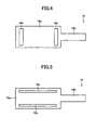
- the upper-electrode body portion may have an inactive portion in the form of a through-hole or a cutout.
- a region where an applied electric field is weak is formed in the piezoelectric/ectrostrictive active portion, which is a portion of the piezoelectric/electrostrictive film sandwiched between the upper-electrode body portion and the lower electrode.
- the thin-walled diaphragm portion and the upper-electrode body portion are formed such that an aspect ratio, which is the ratio of length to width, is about 1.2 or greater.
- FIG. 1 is a view showing the configuration of a piezoelectric/electrostrictive film element 10 for use in a fluid sensor according to an embodiment of the present invention.
- FIG. 1(A) is a plan view of the piezoelectric/electrostrictive film element 10 of the present embodiment.
- FIG. 1(B) is a sectional view taken along line B-B of FIG. 1(A).
- FIG. 1(C) is a sectional view taken along line C-C of FIG. 1(A) .
- the piezoelectric/electrostrictive film element 10 includes a substrate 11.
- the substrate 11 has a thin-walled diaphragm portion 11a.
- the thin-walled diaphragm portion 11a has a substantially rectangular planar shape for simplifying a resonance mode to be excited.
- the thin-walled diaphragm portion 11 a is configured to be able to be flexurally deformed while a first end 11a1 and a second end 11 a2 with respect to its length direction L, and opposite side ends 11 a3 with respect to its width direction W serve as fixed ends.
- the thin-walled diaphragm portion 11a has a thickness of 50 ⁇ m or less, preferably 30 ⁇ m or less, more preferably 15 ⁇ m or less.
- the substrate 11 has a thick portion 11b formed around the thin-walled diaphragm portion 11a.
- the thick portion 11b and the thin-walled diaphragm portion 11 a are seamlessly integral with each other.
- the thick portion 11 b is formed sufficiently thick as compared with the thin-walled diaphragm portion 11a.
- a heat resistant, chemically stable, electrically insulative material is used to form the substrate 11.
- the substrate 11 is formed of a material selected from among, for example, aluminum oxide, magnesium oxide, mullite, aluminum nitride, silicon nitride, glass, and stabilized zirconium oxide. Of these materials, stabilized zirconium oxide can be preferably used to form the substrate 11, since, even when the thin-walled diaphragm portion 11a is formed thin, it maintains high mechanical strength and exhibits excellent toughness.
- the substrate 11 has a cavity 11c and through-holes 11d.
- the cavity 11c is a hollow portion of the piezoelectric/electrostrictive film 10 of the present embodiment which receives therein an object fluid of sensing.
- the cavity 11c is formed at a position corresponding to the thin-walled diaphragm portion 11a.
- the through-holes 11d extend along the thickness direction of the substrate 11. The through-holes 11d are provided in such a manner as to open at the lower surface of the substrate 11, thereby establishing communication between the cavity 11c and the rear side of the substrate 11.
- a lower electrode 12 is formed on the upper surface of the substrate 11 in such a manner as to extend over the thin-walled diaphragm portion 11 a and the thick portion 11 b. Specifically, the lower electrode 12 is formed in a region ranging from the thick portion 11b adjacent to the first end 11a1 of the thin-walled diaphragm portion 11a to a position located toward the first end 11a1 from the second end 11a2 of the thin-walled diaphragm portion 11a. The lower electrode 12 is fixedly bonded to the upper surface of the substrate 11, thereby being provided unitarily with the substrate 11.
- the lower electrode 12 is formed of an electrode material which contains, as a main component, platinum, palladium, rhodium, silver, or an alloy thereof.
- the lower electrode 12 is formed by any of various known film formation processes (for example, thin-film formation processes, such as ion beam process, sputtering, vacuum deposition, CVD, ion plating, and plating, and thick-film formation processes, such as screen printing, spraying, and dipping).
- An auxiliary electrode 13 is formed on the upper surface of the substrate 11 in such a manner as to extend over the thick portion 11 b and the second end 11a2 of the thin-walled diaphragm portion 11a. Specifically, the auxiliary electrode 13 is formed in a region ranging from the thick portion 11 b adjacent to the second end 11 a2 of the thin-walled diaphragm portion 11 a to a position located toward the first end 11a1 from the second end 11a2 of the thin-walled diaphragm portion 11a. The auxiliary electrode 13 is also fixedly bonded to the upper surface of the substrate 11, thereby being provided unitarily with the substrate 11.
- the auxiliary electrode 13 and the lower electrode 12 are provided on substantially the same plane.
- a predetermined gap 14 is provided between the auxiliary electrode 13 and the lower electrode 12 for electrically insulating them from each other. That is, the auxiliary electrode 13 is provided in such a manner as to be separated from the lower electrode 12 across the gap 14.
- the gap 14 is provided at a position located toward the first end 11a1 from the second end 11a2 of the thin-walled diaphragm portion 11a; in other words, on the thin-walled diaphragm portion 11a.
- the auxiliary electrode 13 is formed of an electrode material which contains, as a main component, platinum, palladium, rhodium, silver, or an alloy thereof.
- the auxiliary electrode 13 is formed by any of various known film formation processes mentioned above.
- a piezoelectric/electrostrictive film 15 is formed on the lower electrode 12 and the auxiliary electrode 13 so as to extend over the lower electrode 12 and the auxiliary electrode 13.
- the piezoelectric/electrostrictive film 15 is provided in such a manner as to project beyond opposite end portions of the lower electrode 12 with respect to the width direction W.
- the piezoelectric/electrostrictive film 15 is fixedly bonded onto the lower electrode 12 and the auxiliary electrode 13, thereby being provided unitarily with the lower electrode 12 and the auxiliary electrode 13.
- the piezoelectric/electrostrictive film 15 is formed by any of various known film formation processes.
- the piezoelectric/electrostrictive film 15 is formed such that an end portion of the lower electrode 12 and an end portion of the auxiliary electrode 13 are exposed on the thick wall portion 11 b from its opposite end portions along the length direction L.
- the end portions of the lower electrode 12 and the auxiliary electrode 13 exposed on the thick portion 11 b serve as terminals for lead connection.
- the piezoelectric/electrostrictive film 15 is formed from a material selected from among: lead-based ceramic piezoelectric/electrostrictive materials, such as lead zirconate, lead titanate, and lead zirconate titanate (PZT); barium titanate, and barium titanate ceramic ferroelectrics which contain barium titanate as a main component; polymeric piezoelectrics as typified by polyvinylidene fluoride (PVDF); and Bi ceramic piezoelectrics as typified by (Bi 0.5 Na 0.5 )TiO 3 .
- PZT piezoelectrics are most preferably used, because of high piezoelectric characteristics, which enable high-sensitivity detection.
- the piezoelectric/electrostrictive film 15 includes a piezoelectric/electrostrictive active portion 15a, an incomplete bond portion 15b, overhang portions 15c, and incomplete bond portions 15d.
- the piezoelectric/electrostrictive active portion 15a is a portion sandwiched between the lower electrode 12 and an upper-electrode body portion 16a, which is a major portion of an upper electrode 16 formed on the piezoelectric/electrostrictive film 15.
- the piezoelectric/electrostrictive active portion 15a is provided only on the thin-walled diaphragm portion 11a.
- the incomplete bond portion 15b is provided in such a manner as to project into the gap 14.
- the incomplete bond portion 15b is incompletely bonded to the substrate 11 (in an incompletely bonded state).
- the incomplete bond portion 15b is incompletely bonded to the substrate 11 such that the peel strength from the substrate 11 is 0.5 kg/mm 2 or less.
- the overhang portions 15c are end portions of the piezoelectric/electrostrictive film 15 with respect to the width direction W and are provided in such a manner as to laterally project beyond the upper electrode 16.
- the incomplete bond portions 15d are provided under the overhang portions 15c and laterally cover the lower electrode 12. Similarly to the above-mentioned incomplete bond portion 15b, the incomplete bond portions 15d are incompletely bonded to the substrate 11.
- the above-mentioned upper electrode 16 is provided in such a manner as to extend over the piezoelectric/electrostrictive 15 and the auxiliary electrode 13.
- the upper electrode 16 is fixedly bonded onto the piezoelectric/electrostrictive film 15 and the auxiliary electrode 13, thereby being provided unitarily with the piezoelectric/electrostrictive film 15 and the auxiliary electrode 13.
- the upper electrode 16 is formed from an electrically conductive material having high bondability in relation to the piezoelectric/electrostrictive film 15 by a film formation process similar to that used to form the lower electrode 12 and the auxiliary electrode 13.
- the upper electrode 16 is composed of the upper-electrode body portion 16a and a connection portion 16b.
- the upper-electrode body portion 16a is disposed in such a manner as to face the thin-walled diaphragm portion 11 a with the lower electrode 12 and the piezoelectric/electrostrictive film 15 intervening therebetween.
- the upper-electrode body portion 16a has a planar shape generally similar to that of the thin-walled diaphragm portion 11 a.
- connection portion 16b has a width narrower than that of the upper-electrode body portion 16a.
- the connection portion 16b is provided on the piezoelectric/electrostrictive film 15 and the auxiliary electrode 13 so as to connect the upper-electrode body portion 16a and the auxiliary electrode 13. That is, an end portion of the connection portion 16b is seamlessly integral with the upper-electrode body portion 16a so as to be connected with the upper-electrode body portion 16a.
- the other end portion of the connection portion 16b is bonded to the auxiliary electrode 13, thereby being electrically connected to the auxiliary electrode 13.
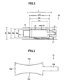
- FIG. 2 is a plan view of the piezoelectric/electrostrictive film element 10 shown in FIG. 1 and corresponds to FIG. 1(A) .
- the upper-electrode body portion 16a (along with the thin-walled diaphragm portion 11a) is formed such that an aspect ratio, which is the ratio of length to width, is about 1.2 or greater.
- the thin-walled diaphragm portion 11a and the piezoelectric/electrostrictive film 15 are formed such that the ratio (Wd/Wp) of a piezoelectric/electrostrictive-film width Wp to the thin-walled-diaphragm-portion width Wd is 0.95 or less and such that the ratio (Ld/Lp) of a piezoelectric/electrostrictive-film length Lp to the thin-walled-diaphragm-portion length Ld is 0.95 or less. That is, as viewed in plane, a major portion (piezoelectric/electrostrictive active portion 15a in FIG. 1 ) of the piezoelectric/electrostrictive film 15 is located at the inside of the outline of the thin-walled diaphragm portion 11 a.
- an auxiliary connection portion 17 is provided independently of the connection portion 16b for connecting the upper-electrode body portion 16a and the auxiliary electrode 13. That is, in the piezoelectric/electrostrictive film element 10 of the present embodiment, the upper electrode 16 and the auxiliary electrode 13 are electrically connected through a plurality of independent paths.
- the auxiliary connection portion 17 is disposed a greatest possible distance apart from the connection portion 16b.
- the lower electrode 12 and the auxiliary electrode 13 are formed, by a screen printing process, on the upper surface of the substrate 11 having a predetermined shape mentioned above.
- a dummy layer is formed, by a screen printing process, on the upper surface of the substrate 11 at positions corresponding to the incomplete bond portions 15b and 15d so as to prevent direct contact between the substrate 11 and the piezoelectric/electrostrictive film 15.
- the dummy layer is a film of a synthetic resin and is ablated by burning in thermal processing, which will be described later, for sintering the piezoelectric/electrostrictive film 15.
- the piezoelectric/electrostrictive film 15 is formed through an application step which employs a screen printing process, and a thermal processing step for sintering a film applied in the application step. At this time, the above-mentioned dummy layer is ablated, whereby the incomplete bond portions 15b and 15d are formed.
- the upper electrode 16 is formed by a screen printing process. Then, a laminate of the upper electrode 16, the piezoelectric/electrostrictive film 15, the auxiliary electrode 13, the lower electrode 12, and the substrate 11 is subjected to thermal processing. By this procedure, the layers of the laminate are firmly bonded and united together.
- a predetermined high voltage is applied between the upper electrode 16 and the lower electrode 12 for polarization of the piezoelectric/electrostrictive film 15.
- Fluid to be measured is introduced into the cavity 11c through the through-holes 11d. Fluid which has undergone measurement in the cavity 11c is discharged from the cavity 11c through the through-holes 11d.
- the piezoelectric/electrostrictive active portion 15a of the piezoelectric/electrostrictive film 15 is deformed by converse piezoelectric effect.
- the deformation of the piezoelectric/electrostrictive film 15 causes the thin-walled diaphragm portion 11a to flexurally deform.
- the thin-walled diaphragm portion 11a is excited at a predetermined resonance frequency.
- Fluid contained in the cavity 11c imposes viscous resistance on vibration of the thin-walled diaphragm portion 11a.
- a vibrating condition of the thin-walled diaphragm portion 11a under the influence of the viscous resistance and variation of the vibrating condition caused by the viscous resistance appear in the form of an expanding-and-contracting condition of the piezoelectric/electrostrictive active portion 15a of the piezoelectric/electrostrictive film 15 sandwiched between the upper electrode 16 and the lower electrode 12 and in the form of variation of the expanding-and-contracting condition.
- the expanding-and-contracting condition of the piezoelectric/electrostrictive active portion 15a and variation of the expanding-and-contracting condition appear in the form of a waveform of an output voltage generated between the upper electrode 16 and the lower electrode 12 and in the form of variation of the waveform.
- a characteristic of the fluid-to-be-measured introduced into the cavity 11c can be determined.
Landscapes
- Physics & Mathematics (AREA)
- General Physics & Mathematics (AREA)
- Chemical & Material Sciences (AREA)
- General Health & Medical Sciences (AREA)
- Health & Medical Sciences (AREA)
- Life Sciences & Earth Sciences (AREA)
- Analytical Chemistry (AREA)
- Biochemistry (AREA)
- Immunology (AREA)
- Pathology (AREA)
- Ceramic Engineering (AREA)
- Engineering & Computer Science (AREA)
- Acoustics & Sound (AREA)
- General Electrical Machinery Utilizing Piezoelectricity, Electrostriction Or Magnetostriction (AREA)
- Piezo-Electric Transducers For Audible Bands (AREA)
- Particle Formation And Scattering Control In Inkjet Printers (AREA)
Applications Claiming Priority (2)
| Application Number | Priority Date | Filing Date | Title |
|---|---|---|---|
| JP2006119580 | 2006-04-24 | ||
| PCT/JP2007/059283 WO2007123278A1 (fr) | 2006-04-24 | 2007-04-23 | Dispositif de film piézo-électrique |
Publications (3)
| Publication Number | Publication Date |
|---|---|
| EP2020692A1 true EP2020692A1 (fr) | 2009-02-04 |
| EP2020692A4 EP2020692A4 (fr) | 2012-09-12 |
| EP2020692B1 EP2020692B1 (fr) | 2014-05-14 |
Family
ID=38625167
Family Applications (1)
| Application Number | Title | Priority Date | Filing Date |
|---|---|---|---|
| EP07742718.5A Expired - Fee Related EP2020692B1 (fr) | 2006-04-24 | 2007-04-23 | Dispositif de film piézo-électrique |
Country Status (5)
| Country | Link |
|---|---|
| US (1) | US7755253B2 (fr) |
| EP (1) | EP2020692B1 (fr) |
| JP (1) | JP5031737B2 (fr) |
| CN (1) | CN101427393B (fr) |
| WO (1) | WO2007123278A1 (fr) |
Families Citing this family (8)
| Publication number | Priority date | Publication date | Assignee | Title |
|---|---|---|---|---|
| JP5006354B2 (ja) | 2009-01-29 | 2012-08-22 | 日本碍子株式会社 | 圧電/電歪共振子 |
| KR101622681B1 (ko) | 2013-02-28 | 2016-05-31 | 닛테쓰 스미킨 고한 가부시키가이샤 | 알루미늄 함유 아연계 도금 강판 및 그 제조 방법 |
| CN205810862U (zh) | 2013-03-11 | 2016-12-14 | 苹果公司 | 便携式电子设备及用于便携式电子设备的振动器组件 |
| US10164688B2 (en) | 2014-04-30 | 2018-12-25 | Apple Inc. | Actuator assisted alignment of connectible devices |
| JP6314777B2 (ja) * | 2014-09-30 | 2018-04-25 | セイコーエプソン株式会社 | 超音波センサー並びにプローブおよび電子機器 |
| US11334164B2 (en) | 2019-07-22 | 2022-05-17 | Apple Inc. | Portable electronic device having a haptic device with a moving battery element |
| KR102621578B1 (ko) * | 2021-04-13 | 2024-01-05 | 서강대학교 산학협력단 | 입자의 밀도 측정 장치 및 방법 |
| US20230224387A1 (en) | 2022-01-10 | 2023-07-13 | Apple Inc. | Handheld electronic device |
Family Cites Families (10)
| Publication number | Priority date | Publication date | Assignee | Title |
|---|---|---|---|---|
| JP2692397B2 (ja) * | 1991-02-25 | 1997-12-17 | 日本電気株式会社 | 電歪効果素子 |
| JP3151644B2 (ja) * | 1993-03-08 | 2001-04-03 | 日本碍子株式会社 | 圧電/電歪膜型素子 |
| JP3388060B2 (ja) | 1994-11-25 | 2003-03-17 | 日本碍子株式会社 | 流体の特性測定用素子及び流体の特性測定装置 |
| JP3501860B2 (ja) * | 1994-12-21 | 2004-03-02 | 日本碍子株式会社 | 圧電/電歪膜型素子及びその製造方法 |
| JP3728623B2 (ja) * | 2001-03-02 | 2005-12-21 | 日本碍子株式会社 | 圧電/電歪膜型素子 |
| JP3781119B2 (ja) * | 2003-03-17 | 2006-05-31 | セイコーエプソン株式会社 | 圧電デバイス用パッケージ及び圧電デバイス |
| US7126255B2 (en) | 2004-04-05 | 2006-10-24 | Ngk Insulators, Ltd. | Piezoelectric/electrostrictive film-type device |
| JP5009507B2 (ja) * | 2004-04-05 | 2012-08-22 | 日本碍子株式会社 | 圧電/電歪膜型素子 |
| JP5004797B2 (ja) * | 2005-06-29 | 2012-08-22 | 日本碍子株式会社 | 圧電/電歪膜型素子 |
| DE102005051289B3 (de) * | 2005-10-26 | 2007-05-16 | Siemens Ag | Piezoaktor und Verfahren zur Herstellung desselben |
-
2007
- 2007-04-23 JP JP2008512200A patent/JP5031737B2/ja not_active Expired - Fee Related
- 2007-04-23 CN CN2007800145051A patent/CN101427393B/zh not_active Expired - Fee Related
- 2007-04-23 WO PCT/JP2007/059283 patent/WO2007123278A1/fr not_active Ceased
- 2007-04-23 EP EP07742718.5A patent/EP2020692B1/fr not_active Expired - Fee Related
-
2008
- 2008-09-30 US US12/241,455 patent/US7755253B2/en not_active Expired - Fee Related
Also Published As
| Publication number | Publication date |
|---|---|
| US7755253B2 (en) | 2010-07-13 |
| EP2020692A4 (fr) | 2012-09-12 |
| CN101427393A (zh) | 2009-05-06 |
| CN101427393B (zh) | 2010-09-01 |
| JP5031737B2 (ja) | 2012-09-26 |
| US20090072667A1 (en) | 2009-03-19 |
| WO2007123278A1 (fr) | 2007-11-01 |
| EP2020692B1 (fr) | 2014-05-14 |
| JPWO2007123278A1 (ja) | 2009-09-10 |
Similar Documents
| Publication | Publication Date | Title |
|---|---|---|
| US7755253B2 (en) | Piezoelectric element and shape of an elecrode thereof | |
| US7427820B2 (en) | Piezoelectric/electrostrictive film element | |
| JP3482939B2 (ja) | 圧電/電歪膜型素子 | |
| JP3465675B2 (ja) | 圧電/電歪膜型素子 | |
| CN1780010B (zh) | 压电/电致伸缩器件 | |
| JPWO1999013300A1 (ja) | 質量センサおよび質量検出方法 | |
| US7183694B2 (en) | Piezoelectric/electrostrictive device | |
| US6541895B2 (en) | Piezoelectric/electrostrictive film element | |
| US7126255B2 (en) | Piezoelectric/electrostrictive film-type device | |
| JP5009507B2 (ja) | 圧電/電歪膜型素子 | |
| JP4936909B2 (ja) | 流体特性測定装置の使用方法 | |
| US7876023B2 (en) | Piezoelectric/electrostrictive membrane sensor |
Legal Events
| Date | Code | Title | Description |
|---|---|---|---|
| PUAI | Public reference made under article 153(3) epc to a published international application that has entered the european phase |
Free format text: ORIGINAL CODE: 0009012 |
|
| 17P | Request for examination filed |
Effective date: 20081016 |
|
| AK | Designated contracting states |
Kind code of ref document: A1 Designated state(s): AT BE BG CH CY CZ DE DK EE ES FI FR GB GR HU IE IS IT LI LT LU LV MC MT NL PL PT RO SE SI SK TR |
|
| AX | Request for extension of the european patent |
Extension state: AL BA HR MK RS |
|
| DAX | Request for extension of the european patent (deleted) | ||
| RBV | Designated contracting states (corrected) |
Designated state(s): DE FR GB |
|
| A4 | Supplementary search report drawn up and despatched |
Effective date: 20120809 |
|
| RIC1 | Information provided on ipc code assigned before grant |
Ipc: H01L 41/113 20060101ALI20120803BHEP Ipc: H01L 41/047 20060101ALI20120803BHEP Ipc: H01L 41/09 20060101AFI20120803BHEP |
|
| 17Q | First examination report despatched |
Effective date: 20130626 |
|
| GRAP | Despatch of communication of intention to grant a patent |
Free format text: ORIGINAL CODE: EPIDOSNIGR1 |
|
| INTG | Intention to grant announced |
Effective date: 20131128 |
|
| GRAS | Grant fee paid |
Free format text: ORIGINAL CODE: EPIDOSNIGR3 |
|
| GRAA | (expected) grant |
Free format text: ORIGINAL CODE: 0009210 |
|
| AK | Designated contracting states |
Kind code of ref document: B1 Designated state(s): DE FR GB |
|
| REG | Reference to a national code |
Ref country code: GB Ref legal event code: FG4D |
|
| REG | Reference to a national code |
Ref country code: DE Ref legal event code: R096 Ref document number: 602007036710 Country of ref document: DE Effective date: 20140618 |
|
| REG | Reference to a national code |
Ref country code: DE Ref legal event code: R097 Ref document number: 602007036710 Country of ref document: DE |
|
| PLBE | No opposition filed within time limit |
Free format text: ORIGINAL CODE: 0009261 |
|
| STAA | Information on the status of an ep patent application or granted ep patent |
Free format text: STATUS: NO OPPOSITION FILED WITHIN TIME LIMIT |
|
| 26N | No opposition filed |
Effective date: 20150217 |
|
| REG | Reference to a national code |
Ref country code: DE Ref legal event code: R097 Ref document number: 602007036710 Country of ref document: DE Effective date: 20150217 |
|
| REG | Reference to a national code |
Ref country code: DE Ref legal event code: R119 Ref document number: 602007036710 Country of ref document: DE |
|
| GBPC | Gb: european patent ceased through non-payment of renewal fee |
Effective date: 20150423 |
|
| PG25 | Lapsed in a contracting state [announced via postgrant information from national office to epo] |
Ref country code: DE Free format text: LAPSE BECAUSE OF NON-PAYMENT OF DUE FEES Effective date: 20151103 Ref country code: GB Free format text: LAPSE BECAUSE OF NON-PAYMENT OF DUE FEES Effective date: 20150423 |
|
| REG | Reference to a national code |
Ref country code: FR Ref legal event code: ST Effective date: 20151231 |
|
| PG25 | Lapsed in a contracting state [announced via postgrant information from national office to epo] |
Ref country code: FR Free format text: LAPSE BECAUSE OF NON-PAYMENT OF DUE FEES Effective date: 20150430 |