EP2020748A2 - Aktive Clampingschaltung für einen Leistungshalbleiterschalter - Google Patents
Aktive Clampingschaltung für einen Leistungshalbleiterschalter Download PDFInfo
- Publication number
- EP2020748A2 EP2020748A2 EP20080012364 EP08012364A EP2020748A2 EP 2020748 A2 EP2020748 A2 EP 2020748A2 EP 20080012364 EP20080012364 EP 20080012364 EP 08012364 A EP08012364 A EP 08012364A EP 2020748 A2 EP2020748 A2 EP 2020748A2
- Authority
- EP
- European Patent Office
- Prior art keywords
- transistor
- clamping circuit
- switch
- node
- input
- Prior art date
- Legal status (The legal status is an assumption and is not a legal conclusion. Google has not performed a legal analysis and makes no representation as to the accuracy of the status listed.)
- Withdrawn
Links
- 239000004065 semiconductor Substances 0.000 title claims description 18
- 230000004913 activation Effects 0.000 claims abstract description 17
- 239000003990 capacitor Substances 0.000 claims description 7
- 230000001681 protective effect Effects 0.000 description 5
- 230000001133 acceleration Effects 0.000 description 2
- 230000003071 parasitic effect Effects 0.000 description 2
- 230000003213 activating effect Effects 0.000 description 1
- 230000008901 benefit Effects 0.000 description 1
- 230000008859 change Effects 0.000 description 1
- 230000009849 deactivation Effects 0.000 description 1
- 238000010586 diagram Methods 0.000 description 1
- 230000009977 dual effect Effects 0.000 description 1
- 230000000694 effects Effects 0.000 description 1
- 230000005669 field effect Effects 0.000 description 1
- 230000009467 reduction Effects 0.000 description 1
Images
Classifications
-
- H—ELECTRICITY
- H03—ELECTRONIC CIRCUITRY
- H03K—PULSE TECHNIQUE
- H03K17/00—Electronic switching or gating, i.e. not by contact-making and –breaking
- H03K17/06—Modifications for ensuring a fully conducting state
-
- H—ELECTRICITY
- H03—ELECTRONIC CIRCUITRY
- H03K—PULSE TECHNIQUE
- H03K17/00—Electronic switching or gating, i.e. not by contact-making and –breaking
- H03K17/08—Modifications for protecting switching circuit against overcurrent or overvoltage
- H03K17/081—Modifications for protecting switching circuit against overcurrent or overvoltage without feedback from the output circuit to the control circuit
- H03K17/0812—Modifications for protecting switching circuit against overcurrent or overvoltage without feedback from the output circuit to the control circuit by measures taken in the control circuit
- H03K17/08128—Modifications for protecting switching circuit against overcurrent or overvoltage without feedback from the output circuit to the control circuit by measures taken in the control circuit in composite switches
-
- H—ELECTRICITY
- H03—ELECTRONIC CIRCUITRY
- H03K—PULSE TECHNIQUE
- H03K17/00—Electronic switching or gating, i.e. not by contact-making and –breaking
- H03K17/16—Modifications for eliminating interference voltages or currents
- H03K17/168—Modifications for eliminating interference voltages or currents in composite switches
-
- H—ELECTRICITY
- H03—ELECTRONIC CIRCUITRY
- H03K—PULSE TECHNIQUE
- H03K17/00—Electronic switching or gating, i.e. not by contact-making and –breaking
- H03K17/06—Modifications for ensuring a fully conducting state
- H03K2017/066—Maximizing the OFF-resistance instead of minimizing the ON-resistance
-
- H—ELECTRICITY
- H03—ELECTRONIC CIRCUITRY
- H03K—PULSE TECHNIQUE
- H03K2217/00—Indexing scheme related to electronic switching or gating, i.e. not by contact-making or -breaking covered by H03K17/00
- H03K2217/0036—Means reducing energy consumption
Definitions
- the invention relates to an active clamping circuit for a reference to a reference potential switching input of a power semiconductor switch.
- a power semiconductor switch e.g. An IGBT is used to switch large voltages and currents.
- the power semiconductor switch is driven at its switching input by a control signal. This is generated by a driver circuit - short driver. If the control signal of the driver fails, e.g. if this is not supplied with energy, in unfavorable cases, the switching state of the power semiconductor switch may be undefined.
- Undefined means that it is then not certain whether the IGBT switches on or off or remains in the current switching state. Unintentional switching of the IGBT happens, for example, when the switching input connected to the gate of the IGBT charges via a parasitic capacitance of the power semiconductor switch, in the case of the IGBT, for example, the Miller capacitance between collector and gate. Such charging occurs, for example, when the voltage at the collector of the IBGT changes over time due to an external voltage source. This in turn can be done, for example, by parallel-connected IGBTs, which switch the intermediate circuit voltage in an eg converter circuit.
- the disadvantage here is that the lower the resistance value, the power loss caused by it increases during normal operation of the IGBT. In normal operation is compared to the reference potential voltage at the switching input, which generates a current flow and thus a power loss through the protective resistor. A reduction of the resistance value of the protective resistor is therefore only up to a certain extent, depending on the application, economically possible.
- the object of the present invention is to propose an improved clamping circuit for the switching input of a power semiconductor switch.
- an active clamping circuit for a switching input of a semiconductor switch, wherein the switching input is related to a reference potential.
- a reference potential is usually ground.
- the active clamp circuit has a node connectable to the switch input and a resistor element leading from the node to the reference potential.
- the clamping circuit also has a Activation input on. Through the activation input, the clamping circuit is switchable to an activated or non-activated state and therefore an active circuit. In the non-activated state, the resistance element has a first resistance value. When activated, the resistance element has a second resistance value which is higher than the first resistance value.
- the clamping circuit is thus in the non-activated state, when e.g. is de-energized, low impedance towards the reference potential.
- activation which is usually done in normal operation of the semiconductor switch, i. when a switching signal from the driver is provided, the clamping circuit between the switching input and the reference potential is switched to high impedance.
- the clamping circuit can be switched to high impedance in order to drastically reduce a current flow from the switching input to the reference potential and the associated power loss.
- the resistance element may have a resistor connected to the node and leading to the reference potential ohmic resistance in the region of the second resistance value.
- the clamping circuit then additionally contains a bypass circuit for the resistor, which is conductive in the non-activated state of the resistance element and is locked in the activated state. In the activated state, that is, when the bypass circuit is disabled, only the ohmic resistance forms a Connection from the node to the reference potential. The clamping circuit thus has the second resistance value. In the non-activated state, the bypass circuit is conductive, thus bypasses the first resistor and forms by its own resistance in about the first, lower resistance, which thus leads from the node to the reference potential.
- the bypass circuit may include at least one first transistor, which is connected with its collector at the node and with its base at the end remote from the node of the resistor. The emitter of the transistor leads to the reference potential. The bypass circuit then also contains a switch leading from the resistor or the base of the first transistor to the reference potential.
- the inclusion of the transistor and the switch creates a clamping circuit, which is in the case of an open-circuiting switching input low resistance to the reference potential and can be switched high impedance by closing the switch between the switching input and reference potential. Namely, if the switch is opened, arises when applying a voltage or charge at the switching input with respect to the reference potential by the self-switching behavior of the transistor via the collector and emitter, a low-resistance connection to the reference potential having the first resistance value. If, in contrast, the switch is closed, the base of the transistor is at the reference potential, the transistor blocks and a current flow from the switching input is only possible via the resistor.
- the resistor is in this case of high impedance, ie in the range of the second resistance value dimensioned.
- the switch may include a second transistor.
- the switch is then also implemented in semiconductor form, mechanical components are avoided, the entire clamping circuit is thereby purely electronic.
- the first transistor may also be part of a transistor cascade in the manner of a Darlington transistor.
- a plurality of first transistors are present in the clamping circuit, which produce depending on the switching state of the switch low-impedance or high-impedance connection between the switching input and reference potential.
- a transistor arrangement in the manner of a Darlington transistor has a very high gain, whereby the resistance, ie the protective resistance, can be selected to be greater, resulting in lower losses during normal operation.
- each transistor of the transistor cascade can then be assigned a separate switch, wherein all switches are equal switching.
- the switches can again contain transistors themselves.
- the resistor may be connected in parallel with a capacitor.
- the capacitor then acts as an acceleration capacitor and, with a rapid change in the voltage at the switching input, amplifies the current into the base of the first transistor (s).
- the node may be connectable to the input via a diode. Assuming a normally positive switch-on voltage relative to the reference potential, the diode thus decouples the clamping circuit from the switch input, so that no negative Voltage when the power semiconductor switch is switched off, in particular when the IGBT is switched off (negative voltage with respect to the reference potential) at the base of the first transistor.
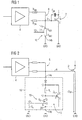
- Fig. 1 shows as a semiconductor switch IGBT 2, which is driven by a driver 4 to turn this on and off.
- the driver 4 has an output 6, which is connected to the input 8 of the IGBT 2.
- an active clamping circuit 10 is also connected, which leads to the ground GND, which also represents the reference potential for the IGBT 2. This is in fact switched on or off via its input 8 with respect to this reference potential.
- the clamping circuit 10 includes a resistance element 11 and has two operating states, which are switchable via an activation input 12. In the inactive state, the clamping circuit 10 or the resistance element 11 has a first ohmic resistance R GE1 , which is so low resistance that a charge accumulating at the gate G can drain to ground GND.
- the driver 4 is active, ie if it generates a potential at the gate G, a high current would flow through the low-resistance resistor R GE1 due to the potential difference between the input 8 and the ground GND.
- the clamping circuit 10 can therefore be activated by the activation input 12, ie it or the resistance element 11 assumes the significantly increased resistance R GE2 . From the gate G, therefore, significantly less current flows through the clamping circuit 10 to the ground GND, resulting in a significantly reduced power dissipation of the circuit in Fig. 1 leads.
- Fig. 2 shows an embodiment of the clamping circuit 10 between the terminals 14a and b.
- a diode D1 is first connected, which leads via a node 16, a resistor R1 and a node 18 to the drain terminal D a field effect transistor Q3.
- the source S of the transistor Q3 leads via a further node 20 to the terminal 14b.
- the gate G of the transistor Q3 is connected to the activation input 12, or represents this.
- a bipolar transistor Q1 is connected to its collector C at the node 16, with its base B at node 18 and its emitter E at node 20.
- the transistors Q1 and Q3 thus form an activatable by the activation input 12 bypass circuit 13 for the resistor R1.
- the transistor Q3 forms a switch 15 and, in an alternative embodiment, could also be implemented by a mechanical switch 15 which connects the nodes 18 and 20 to a switching command on the activation input 12.
- the clamping circuit 10 If the clamping circuit 10 is not activated, ie if the activation voltage U A at the activation input 12 is 0 V, the transistor Q3 is switched off. This blocks and thus forms an open circuit between the nodes 18 and 20. In the case of a charge on the gate G or input 8, therefore, a current flows through the terminal 14a via the diode D1 and the resistor R1 to the base B of the transistor Q1 and makes it conductive.
- the transistor Q1 is low-impedance between collector C and emitter E and carries the charge or voltage at the input 8 to the node 20 and thus to the ground GND out.
- the volume resistance of the clamping circuit 10 in this case is R GE1 represented by the collector-emitter resistance of the transistor Q1.
- the transistor Q3 Upon application of the activation voltage UA at the activation input 12, the transistor Q3 becomes conductive and forms a low-resistance connection between the nodes 18 and 20. As a result, the base of the transistor Q1 is pulled to ground potential GND, the transistor Q1 blocks, and the input 8 is only one conductive connection via the diode D1 and the resistor R1 to ground GND.
- the resistor R1 is high impedance, and corresponds approximately to the value R GE2 of the clamping circuit 10 between the connection terminals 14a, b. In other words, the activation voltage UA deactivates the current path via the transistor Q1.
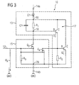
- Fig. 3 shows an alternative embodiment of a clamping circuit 10.
- the circuit consists of a clamping circuit 15, which is composed of the transistors Q1, Q2, the resistors R1, R2 and the capacitor C1.
- the combination of Q1 and Q2 corresponds to that of a very high gain Darlington transistor.
- the circuit for activating and deactivating the gate clamping, that is, the switch 15, consists of the transistors Q3, Q4 and the resistor R3.
- the transistors Q3 and Q4 form a transistor decade 17 in the manner of a Darlington transistor.
- the triggering circuit which generates the voltage UA activates the clamping.
- the two transistors Q 3 and Q 4 are turned off and constitute a high-resistance connection between the bases B of Q 1 , Q 2 and the ground GND.
- a begins Current from a voltage of about the sum of the base-emitter voltages of Q1 and Q2 through R 1 in the base B of Q 2 to flow.
- the transistors Q 1 and Q 2 turn on and thus begin to dissipate the charge at the gate G of the IGBT 2 to ground GND, ie to clamp the voltage at the gate G of the IGBT.
- the circuit acts as a low resistance resistor with a voltage source equal in magnitude to the sum of the base-emitter voltages of Q1 and Q2.
- the capacitor C 1 is an acceleration capacitor and amplifies the base current into the base B of Q 2 when the voltage at the gate G of the IGBT 2 changes rapidly.
- a control voltage U A must be applied so that the switch-on thresholds of the transistors Q 3 and Q 4 are safely exceeded.
- the transistors Q 3 , Q 4 in the example FETs, are turned on.
- the bases B of Q 1 and Q 2 are pulled to ground potential GND.
- the transistors Q 1 and Q 2 are now safely switched off. It is necessary that both bases B of Q 1 and Q 2 are simultaneously pulled to ground GND to ensure a quick turn off and thus deactivation of the clamping circuit, ie the bypass circuit 13.
- the diode D 1 decouples the remaining clamping circuit 10 from the gate G of the IGBT 2 so that no negative voltage is applied to the collectors C of Q 1 and Q 2 when the IGBT 2 is switched off.
Landscapes
- Electronic Switches (AREA)
- Power Conversion In General (AREA)
Abstract
Eine Clampingschaltung (10) für einen auf ein Bezugspotential (GND) bezogenen Schalteingang (8) eines Leistungshalbleiterschalters (2), enthält einen mit dem Schalteingang (8) verbindbaren Knoten (16) und ein vom Knoten (16) zum Bezugspotential (GND) führendes Widerstandselement (11) mit einem Aktivierungseingang (12), das im nicht aktivierten Zustand einen ersten Widerstandswert (R GE1 ) aufweist und im aktivierten Zustand einen zweiten, höheren Widerstandswert (R GE2 ) aufweist.
Description
- Die Erfindung betrifft eine aktive Clampingschaltung für einen auf ein Bezugspotential bezogenen Schalteingang eines Leistungshalbleiterschalters.
- Ein Leistungshalbleiterschalter, z.B. ein IGBT, dient zum Schalten großer Spannungen und Ströme. Um den eigentlichen Schaltvorgang auszulösen, wird der Leistungshalbleiterschalter an seinem Schalteingang durch ein Steuersignal angesteuert. Dieses wird von einer Treiberschaltung - kurz Treiber - generiert. Fällt das Steuersignal des Treibers aus, z.B. wenn dieser nicht mit Energie versorgt wird, kann in ungünstigen Fällen der Schaltzustand des Leistungshalbleiterschalters undefiniert sein.
- Undefiniert heißt, dass dann nicht sichergestellt ist, ob der IGBT ein- oder ausschaltet bzw. im derzeitigen Schaltzustand verbleibt. Ein ungewolltes Schalten des IGBT passiert z.B. dann, wenn sich der mit dem Gate des IGBT verbundene Schalteingang über eine parasitäre Kapazität des Leistungshalbleiterschalters, im Falle des IGBT z.B. die Miller-Kapazität zwischen Kollektor und Gate, auflädt. Eine derartige Aufladung passiert z.B. wenn sich die Spannung am Kollektor des IBGT durch eine externe Spannungsquelle zeitlich ändert. Dies wiederum kann z.B. geschehen durch parallel geschaltete IGBTs, welche die Zwischenkreisspannung in einer z.B. Stromrichterschaltung schalten.
- Eine derartige Situation ist in jedem Fall zu vermeiden. Um ungewolltes Schalten zu verhindern ist es bekannt, den Schalteingang durch einen ohmschen Widerstand bzw. Schutzwiderstand mit dem Bezugspotential des Halbleiterschalters, z.B. Masse, zu verbinden. Eine derartige Schutzbeschaltung des Schalteingangs eines Leistungshalbleiterschalters wird auch passive Clampingschaltung genannt. Der Widerstand der Clampingschaltung darf nicht zu groß sein, damit auch bei großen Spannungsschwankungen dU/dt zwischen Kollektor und Emitter eines IGBT ein Einschalten des IGBT verhindert wird.
- Nachteilig hierbei ist, dass, je niedriger der Widerstandwert ist, die durch ihn verursachte Verlustleistung im Normalbetrieb des IGBT ansteigt. Im Normalbetrieb liegt gegenüber dem Bezugspotential Spannung am Schalteingang, welche über den Schutzwiderstand einen Stromfluss und damit eine Verlustleistung erzeugt. Eine Verkleinerung des Widerstandswertes des Schutzwiederstandes ist daher nur bis zu einem bestimmten Maß, je nach Anwendung, wirtschaftlich möglich.
- Aufgabe der vorliegenden Erfindung ist es, eine verbesserte Clampingschaltung für den Schalteingang eines Leistungshalbleiterschalters vorzuschlagen.
- Die Aufgabe wird gelöst durch eine aktive Clampingschaltung für einen Schalteingang eines Halbleiterschalters, wobei der Schalteingang auf ein Bezugspotential bezogen ist. Ein derartiges Bezugspotential ist in der Regel Masse. Die aktive Clampingschaltung weist einen mit dem Schalteingang verbindbaren Knoten und ein vom Knoten zum Bezugspotential führendes Widerstandselement auf. Die Clampingschaltung weist außerdem einen Aktivierungseingang auf. Durch den Aktivierungseingang ist die Clampingschaltung in einen aktivierten oder in einen nicht aktivierten Zustand schaltbar und daher eine aktive Schaltung. Im nichtaktivierten Zustand weist das Widerstandselement einen ersten Widerstandwert auf. Im aktivierten Zustand weist das Widerstandselemente einen zweiten Widerstandwert auf, der höher ist als der erste Widerstandswert.
- Die Clampingschaltung ist damit im nichtaktivierten Zustand, wenn sie z.B. stromlos ist, niederohmig zum Bezugspotential hin. Durch Aktivierung, die in der Regel im Normalbetrieb des Halbleiterschalters erfolgt, d.h. bei Bereitstellung eines Schaltsignals vom Treiber, wird die Clampingschaltung zwischen Schalteingang und Bezugspotential hochohmig geschaltet.
- Somit ergibt sich bei nichtaktivem Zustand der Vorteil, dass der Schalteingang des Halbleiterschalters niederohmig zum Bezugspotential geführt ist, was einen sicheren und dauerhaften Schaltzustand des Halbleiterschalters garantiert. Im Betrieb des Halbleiterschalters kann die Clampingschaltung hochohmig geschaltet werden, um einen Stromfluss vom Schalteingang zum Bezugspotential und die damit verknüpfte Verlustleistung drastisch zu reduzieren.
- Das Widerstandselement kann einen am Knoten angeschlossenen und zum Bezugspotential führenden ohmschen Widerstand im Bereich des zweiten Widerstandwertes aufweisen. Die Clampingschaltung enthält dann zusätzlich eine Bypassschaltung für den Widerstand, welche im nicht aktivierten Zustand des Widerstandselements leitend ist und im aktivierten Zustand gesperrt ist. Im aktivierten Zustand, wenn also die Bypassschaltung gesperrt ist, bildet lediglich der ohmsche Widerstand eine Verbindung vom Knoten zum Bezugspotential. Die Clampingschaltung weist damit den zweiten Widerstandswert auf. Im nicht aktivierten Zustand ist die Bypassschaltung leitend, überbrückt damit den ersten Widerstand und bildet durch ihren Eigenwiderstand in etwa den ersten, niedrigeren Widerstandswert, welcher damit vom Knoten zum Bezugspotential führt.
- Die Bypassschaltung kann mindestens einen ersten Transistor enthalten, welcher mit seinem Kollektor am Knoten und mit seiner Basis am dem Knoten abgewandten Ende des Widerstands angeschlossen ist. Der Emitter des Transistors führt zum Bezugspotential. Die Bypassschaltung enthält dann auch einen vom Widerstand bzw. der Basis des ersten Transistors zum Bezugspotential führenden Schalter.
- Durch die Aufnahme des Transistors und des Schalters entsteht eine Clampingschaltung, welche im Falle eines leerlaufenden Schalteingangs niederohmig zum Bezugspotential ist und durch Schließen des Schalters zwischen Schalteingang und Bezugspotential hochohmig geschaltet werden kann. Ist nämlich der Schalter geöffnet, so entsteht bei Anliegen einer Spannung bzw. Ladung am Schalteingang bezüglich des Bezugspotentials durch das selbstschaltende Verhalten des Transistors über dessen Kollektor und Emitter eine niederohmige Verbindung zum Bezugspotential, die den ersten Widerstandswert aufweist. Wird dagegen der Schalter geschlossen, liegt die Basis des Transistors auf dem Bezugspotential, der Transistor sperrt und ein Stromfluss vom Schalteingang ist nur über den Widerstand möglich. Der Widerstand wird hierbei hochohmig, also im Bereich des zweiten Widerstandswertes, dimensioniert.
- Der Schalter kann einen zweiten Transistor enthalten. Der Schalter ist dann ebenfalls in Halbleiterform ausgeführt, mechanische Bauelemente werden vermieden, die gesamte Clampingschaltung wird dadurch rein elektronisch.
- Der erste Transistor kann auch Teil einer Transistorkaskade nach Art eines Darlingtontransistors sein. Somit sind in der Clampingschaltung mehrere erste Transistoren vorhanden, welche die je nach Schaltzustand des Schalters niederohmige oder hochohmige Verbindung zwischen Schalteingang und Bezugspotential herstellen. Eine Transistoranordnung nach Art eines Darlingtontransistors besitzt eine sehr hohe Verstärkung wodurch der Widerstand, also der Schutzwiderstand, größer gewählt werden kann und sich hierdurch im Normalbetrieb geringere Verluste ergeben.
- In einem derartigen Fall kann dann jedem Transistor der Transistorkaskade ein eigener Schalter zugeordnet sein, wobei sämtliche Schalter gleichschaltend sind. Auch in diesem Fall können die Schalter natürlich wieder selbst Transistoren enthalten.
- Dem Widerstand kann ein Kondensator parallel geschaltet sein. Der Kondensator wirkt dann als Beschleunigungskondensator und verstärkt bei einer schnellen Änderung der Spannung am Schalteingang den Strom in die Basis des bzw. der ersten Transistoren.
- Der Knoten kann mit dem Eingang über eine Diode verbindbar sein. Eine normalerweise gegenüber dem Bezugspotential positive Einschaltspannung vorausgesetzt, entkoppelt die Diode damit den Clampingschaltkreis vom Schalteingang, so dass keine negative Spannung bei ausgeschaltetem Leistungshalbleiterschalter, insbesondere bei ausgeschaltetem IGBT (negative Spannung gegenüber dem Bezugspotential) an der Basis des ersten Transistors anliegt.
- Für eine weitere Beschreibung der Erfindung wird auf die Ausführungsbeispiele der Zeichnungen verwiesen. Es zeigen, jeweils in einer schematischen Prinzipskizze:
- Fig. 1
- ein Prinzipbild einer erfindungsgemäßen Clampingschaltung,
- Fig. 2
- eine Ausführungsform der Clampingschaltung mit zwei einfachen Transistoren,
- Fig. 3
- eine Ausführungsform der Clampingschaltung mit Darlingtonschaltung und doppelter Transistoransteuerung.
-
Fig. 1 zeigt als Halbleiterschalter einen IGBT 2, welcher von einem Treiber 4 angesteuert wird, um diesen ein- und auszuschalten. Der Treiber 4 weist hierzu einen Ausgang 6 auf, welcher am Eingang 8 des IGBT 2 angeschlossen ist. Am Eingang 8 ist außerdem eine aktive Clampingschaltung 10 angeschlossen, welche zur Masse GND führt, die ebenfalls das Bezugspotential für den IGBT 2 darstellt. Dieser wird nämlich über seinen Eingang 8 bezüglich dieses Bezugspotentials ein- oder ausgeschaltet. - Am IGBT 2 ist dessen parasitäre Millerkapazität CM dargestellt, welche sich zwischen Gate G und Kollektor C befindet. Ist der Treiber 4 inaktiv, z.B. nicht mit Energie versorgt bzw. ist dessen Ausgang 6 hochohmig, hat er keinerlei treibende Wirkung auf den Eingang 8. Ein über die Millerkapazität CM fließender Strom führt daher zur Aufladung des Gate G bzw. Eingangs 8 und eventuell zum ungewollten Schalten des IGBT 2, wenn nicht die Clampingschaltung 10 vorhanden wäre, über welche eine derartige Ladung am Gate G zur Masse GND abfließen kann.
- Die Clampingschaltung 10 enthält ein Widerstandselement 11 und besitzt zwei Betriebszustände, welche über einen Aktivierungseingang 12 schaltbar sind. Im inaktiven Zustand besitzt die Clampingschaltung 10 bzw. das Widerstandselement 11 einen ersten ohmschen Widerstand RGE1, welcher derart niederohmig ist, dass eine sich am Gate G ansammelnde Ladung gegen Masse GND abfließen kann.
- Ist der Treiber 4 jedoch aktiv, d.h. erzeugt dieser ein Potential am Gate G, so würde durch die Potentialdifferenz zwischen Eingang 8 und Masse GND ein hoher Strom über den niederohmigen Widerstand RGE1 fließen. Für einen derartigen Fall ist daher durch den Aktivierungseingang 12 die Clampingschaltung 10 aktivierbar, d.h. sie bzw. das Widerstandselement 11 nimmt den deutlich erhöhten ohmschen Widerstand RGE2 an. Vom Gate G fließt daher durch die Clampingschaltung 10 deutlich weniger Strom zur Masse GND, was zu einer deutlich reduzierten Verlustleistung der Schaltung in
Fig. 1 führt. -
Fig. 2 zeigt eine Ausführungsform der Clampingschaltung 10 zwischen deren Anschlussklemmen 14a und b. Am Eingang 14a ist zunächst eine Diode D1 angeschlossen, welche über einen Knoten 16, einen Widerstand R1 und einen Knoten 18 auf den Drainanschluss D einen Feldeffekttransistors Q3 führt. Die Source S des Transistors Q3 führt über einen weiteren Knoten 20 zur Anschlussklemme 14b. Das Gate G des Transistors Q3 ist mit dem Aktivierungseingang 12 verbunden, bzw. stellt diesen dar. Ein Bipolartransistor Q1 ist mit seinem Kollektor C am Knoten 16, mit seiner Basis B am Knoten 18 und mit seinem Emitter E am Knoten 20 angeschlossen. Die Transistoren Q1 und Q3 bilden so eine durch den Aktivierungseingang 12 aktivierbare Bypassschaltung 13 für den Widerstand R1. - Der Transistor Q3 bildet einen Schalter 15 und könnte in einer alternativen Ausführungsform auch durch einen mechanischen Schalter 15 ausgeführt sein, der die Knoten 18 und 20 auf einen Schaltbefehl am Aktivierungseingang 12 verbindet.
- Ist die Clampingschaltung 10 nicht aktiviert, d.h. ist die Aktivierungsspannung UA am Aktivierungseingang 12 gleich 0V, ist der Transistor Q3 ausgeschaltet. Dieser sperrt und bildet somit zwischen den Knoten 18 und 20 einen Leerlauf. Im Falle einer Ladung auf dem Gate G bzw. Eingang 8 fließt daher ein Strom durch die Anschlussklemme 14a über die Diode D1 und den Widerstand R1 auf die Basis B des Transistors Q1 und macht diesen leitend. Der Transistor Q1 wird zwischen Kollektor C und Emitter E niederohmig und führt die Ladung bzw. Spannung am Eingang 8 zum Knoten 20 und damit zur Masse GND hin ab. Der Durchgangswiderstand der Clampingschaltung 10 ist in diesem Fall RGE1, dargestellt durch den Kollektor-Emitterwiderstand des Transistors Q1.
- Bei Anlegen der Aktivierungsspannung UA am Aktivierungseingang 12 wird der Transistor Q3 leitend und bildet eine niederohmige Verbindung zwischen den Knoten 18 und 20. Dadurch wird die Basis des Transistors Q1 auf Massepotential GND gezogen, der Transistor Q1 sperrt, und vom Eingang 8 besteht lediglich noch eine leitende Verbindung über die Diode D1 und den Widertand R1 zur Masse GND. Der Widerstand R1 ist dabei hochohmig, und entspricht in etwa dem Wert RGE2 der Clampingschaltung 10 zwischen den Anschlussklemmen 14a,b. Mit anderen Worten deaktiviert die Aktivierungsspannung UA den Stromweg über den Transistor Q1.
-
Fig. 3 zeigt eine alternative Ausführungsform einer Clampingschaltung 10. Die Schaltung besteht aus einem ClampingSchaltkreis bzw. Bypassschaltung 15, der aus den Transistoren Q1, Q2, den Widerständen R1, R2 und der Kapazität C1 aufgebaut ist. Hier entspricht die Kombination aus Q1 und Q2 der eines Darlington-Transistors mit sehr hoher Verstärkung. Der Schaltkreis zur Aktivierung und Deaktivierung des Gate-Clamping, also der Schalter 15, besteht aus den Transistoren Q3, Q4 und dem Widerstand R3. Die Transistoren Q3 und Q4 bilden eine Transistordekade 17 nach Art eines Darlington-Transistors. - Wird der Treiber 4 z.B. nicht mit Spannung versorgt, hat der ansteuernde Schaltkreis, der die Spannung UA erzeugt, das Clamping aktiviert. Ist also keine Spannung über R3 vorhanden, sind die beiden Transistoren Q3 und Q4 ausgeschaltet und stellen eine hochohmige Verbindung zwischen den Basen B von Q1, Q2 und der Masse GND dar. Steigt nun die Spannung UGE, so beginnt ein Strom ab einer Spannung von ca. der Summe der Basis-Emitterspannungen von Q1 und Q2 durch R1 in die Basis B von Q2 zu fließen. Die Transistoren Q1 und Q2 schalten ein und beginnen somit die Ladung am Gate G des IGBT 2 nach Masse GND abzuführen, d.h. die Spannung am Gate G des IGBT zu klemmen. Der Schaltkreis wirkt wie ein niederohmiger Widerstand mit einer Spannungsquelle der Höhe der Summe der Basis-Emitterspannungen von Q1 und Q2 in Reihe.
- Der Kondensator C1 ist ein Beschleunigungskondensator und verstärkt bei schneller Änderung der Spannung am Gate G des IGBT 2 den Basisstrom in die Basis B von Q2.
- Zur Deaktivierung des Clampings muss eine Steuerspannung UA angelegt werden, so dass die Einschaltschwellen der Transistoren Q3 und Q4 sicher überschritten werden. Die Transistoren Q3, Q4, im Beispiel FETs, werden eingeschaltet. Somit werden die Basen B von Q1 und Q2 auf Massepotential GND gezogen. Die Transistoren Q1 und Q2 sind nun sicher ausgeschaltet. Es ist notwendig, dass beide Basen B von Q1 und Q2 gleichzeitig auf Masse GND gezogen werden um ein schnelles Ausschalten und damit Deaktivieren des Clamping-Schaltkreises, also der Bypassschaltung 13, zu gewährleisten.
- Im so entstehenden deaktivierten Zustand der Clampingschaltung 10 wirkt nur noch der Widerstand R1, der im Beispiel mehrere kQ groß ist, auf das Gate G des IGBT 2. Die im Betrieb entstehende Verlustleistung ist somit vernachlässigbar.
- Die Diode D1 entkoppelt die restliche Clampingschaltung 10 vom Gate G des IGBT 2, so dass keine negative Spannung bei abgeschaltetem IGBT 2 an den Kollektoren C von Q1 und Q2 anliegt.
Claims (8)
- Clampingschaltung (10) für einen auf ein Bezugspotential (GND) bezogenen Schalteingang (8) eines Leistungshalbleiterschalters (2), mit einem mit dem Schalteingang (8) verbindbaren Knoten (16) und einem vom Knoten (16) zum Bezugspotential (GND) führenden Widerstandselement (11) mit einem Aktivierungseingang (12), das im nicht aktivierten Zustand einen ersten Widerstandswert (RGE1) aufweist und im aktivierten Zustand einen zweiten, höheren Widerstandswert (RGE2) aufweist.
- Clampingschaltung (10) nach Anspruch 1, bei dem das Widerstandelement (11) einen am Knoten (16) angeschlossenen und zum Bezugspotential (GND) führenden ohmschen Widerstand (R1) im Bereich des zweiten Widerstandwertes (RGE2), und eine den ersten Widerstandswert (RGE1) aufweisende, im nicht aktivierten Zustand leitende, und im aktivierten Zustand gesperrte Bypassschaltung (13) für den Widerstand (R1) enthält.
- Clampingschaltung (10) nach Anspruch 2, bei dem die Bypassschaltung (13) enthält:- mindestens einen mit seinem Kollektor (C) am Knoten (16) und mit seiner Basis (13) am dem Knoten (16) abgewandten Ende (18) des Widerstands (R1) angeschlossenen ersten Transistor (Q1), dessen Emitter (E) zum Bezugspotential (GND) führt,- einen zwischen Widerstand (R1) und Bezugspotential (GND) angeordneten, im nicht aktivierten Zustand geöffneten, durch den Aktivierungseingang (12) schließbaren Schalter (15).
- Clampingschaltung (10) nach Anspruch 3, bei der der Schalter (15) einen vom Aktivierungseingang (12) angesteuerten zweiten Transistor (Q3) enthält.
- Clampingschaltung (10) nach Anspruch 3 oder 4, bei der der erste Transistor (Q1) Teil einer Transistorkaskade (17) nach Art eines Darlington-Transistors ist.
- Clampingschaltung (10) nach Anspruch 5, bei der jedem Transistor (Q1, Q2) der Transistordekade (17) ein eigener, gleichschaltender Schalter (Q3, Q4) zugeordnet ist.
- Clampingschaltung (10) nach einem der Ansprüche 3 bis 5, mit einem dem Widerstand (R1) parallel geschalteten Kondensator (C1).
- Clampingschaltung (10) nach einem der vorhergehenden Ansprüche, bei der der Knoten (16) mit dem Eingang (8) über eine Diode (D1) verbindbar ist.
Applications Claiming Priority (1)
| Application Number | Priority Date | Filing Date | Title |
|---|---|---|---|
| DE200710036727 DE102007036727A1 (de) | 2007-08-03 | 2007-08-03 | Aktive Clampingschaltung für einen Leistungshalbleiterschalter |
Publications (1)
| Publication Number | Publication Date |
|---|---|
| EP2020748A2 true EP2020748A2 (de) | 2009-02-04 |
Family
ID=40001398
Family Applications (1)
| Application Number | Title | Priority Date | Filing Date |
|---|---|---|---|
| EP20080012364 Withdrawn EP2020748A2 (de) | 2007-08-03 | 2008-07-09 | Aktive Clampingschaltung für einen Leistungshalbleiterschalter |
Country Status (3)
| Country | Link |
|---|---|
| EP (1) | EP2020748A2 (de) |
| CN (1) | CN101394082A (de) |
| DE (1) | DE102007036727A1 (de) |
Cited By (1)
| Publication number | Priority date | Publication date | Assignee | Title |
|---|---|---|---|---|
| EP3849082A1 (de) * | 2020-01-10 | 2021-07-14 | Power Integrations Switzerland GmbH | Klemmschaltung für leistungsschalter |
Families Citing this family (3)
| Publication number | Priority date | Publication date | Assignee | Title |
|---|---|---|---|---|
| CN102856893B (zh) * | 2012-09-21 | 2015-03-18 | 深圳市英威腾电气股份有限公司 | 动态有源嵌位电路和电子设备 |
| US10128248B1 (en) * | 2017-07-14 | 2018-11-13 | Intel Corporation | Aging tolerant apparatus |
| CN112564461A (zh) * | 2019-09-26 | 2021-03-26 | 珠海格力电器股份有限公司 | 一种功率开关电路系统 |
-
2007
- 2007-08-03 DE DE200710036727 patent/DE102007036727A1/de not_active Withdrawn
-
2008
- 2008-07-09 EP EP20080012364 patent/EP2020748A2/de not_active Withdrawn
- 2008-08-01 CN CNA200810176942XA patent/CN101394082A/zh active Pending
Cited By (1)
| Publication number | Priority date | Publication date | Assignee | Title |
|---|---|---|---|---|
| EP3849082A1 (de) * | 2020-01-10 | 2021-07-14 | Power Integrations Switzerland GmbH | Klemmschaltung für leistungsschalter |
Also Published As
| Publication number | Publication date |
|---|---|
| DE102007036727A1 (de) | 2009-02-19 |
| CN101394082A (zh) | 2009-03-25 |
Similar Documents
| Publication | Publication Date | Title |
|---|---|---|
| EP2412096B1 (de) | Jfet-mosfet kaskodeschaltung | |
| DE19902520B4 (de) | Hybrid-Leistungs-MOSFET | |
| EP3281286B1 (de) | Treiberschaltung, schaltungsanordnung umfassend eine treiberschaltung und wechselrichter umfassend eine schaltungsanordnung | |
| DE102012217709A1 (de) | Detektion des nulldurchgangs des laststroms in einer halbleitervorrichtung | |
| EP0039952A1 (de) | Schalter mit einem als Source-Folger betriebenen MIS-FET | |
| DE102014108576A1 (de) | Treiberschaltung mit Miller-Clamping-Funktionalität für Leistungshalbleiterschalter, Leistungshalbleiterschalter und Wechselrichterbrücke | |
| EP0639308A1 (de) | Schaltungsanordnung zum ansteuern eines mos-feldeffekttransistors. | |
| EP2020748A2 (de) | Aktive Clampingschaltung für einen Leistungshalbleiterschalter | |
| EP0817380B1 (de) | Vorrichtung zum Schalten eines induktiven Verbrauchers | |
| EP0361211B1 (de) | Schutzschaltung für einen Leistungshalbleiterbaustein | |
| EP1493229B1 (de) | Schaltungsanordnung zum ansteuern eines halbleiterschalters | |
| EP1987591B1 (de) | Schaltung zum schalten eines spannungsgesteuerten transistors | |
| DE69112153T2 (de) | Pegelumsetzer mit Einzelsteuerung und niedriger dynamischer Impedanz. | |
| DE102010004488B3 (de) | Pegelwandlerschaltung | |
| DE102016223312A1 (de) | Leistungshalbleiterbaugruppe für ein Kraftfahrzeug, Kraftfahrzeug und Verfahren zum Betreiben einer Leistungshalbleiterbaugruppe | |
| DE102016210798B3 (de) | Leistungshalbleiterschaltung | |
| EP4620108A1 (de) | Schaltungsmodul und halbleiterschalter mit einer mehrzahl von in reihe geschalteten schaltungsmodulen | |
| EP0031138B1 (de) | Transistorgegentaktendstufe | |
| DE3536447C2 (de) | Kurzschluß- und überlastfeste Transistorausgangsstufe | |
| WO1998012816A1 (de) | Vorrichtung zur verminderung der kurzschlussamplitude eines abschaltbaren, nichteinrastenden, mos-gesteuerten leistungshalbleiters | |
| DE10243571B4 (de) | Schaltungsanordnung zum Kurzschlussabschalten eines MOSFET-Schalters | |
| EP0555648A2 (de) | Schaltungsanordnung zum Ansteuern von feldgesteuerten Leistungsschaltern | |
| EP0822661A2 (de) | Ansteuerschaltung für ein Feldeffekt gesteuertes Leistungs-Halbleiterbauelement | |
| DE10035387B4 (de) | Stromschaltanordnung | |
| DE102008060793B4 (de) | Schaltungsanordnung zum Schalten einer oder mehrerer induktiver Lasten |
Legal Events
| Date | Code | Title | Description |
|---|---|---|---|
| PUAI | Public reference made under article 153(3) epc to a published international application that has entered the european phase |
Free format text: ORIGINAL CODE: 0009012 |
|
| AK | Designated contracting states |
Kind code of ref document: A2 Designated state(s): AT BE BG CH CY CZ DE DK EE ES FI FR GB GR HR HU IE IS IT LI LT LU LV MC MT NL NO PL PT RO SE SI SK TR |
|
| AX | Request for extension of the european patent |
Extension state: AL BA MK RS |
|
| STAA | Information on the status of an ep patent application or granted ep patent |
Free format text: STATUS: THE APPLICATION IS DEEMED TO BE WITHDRAWN |
|
| 18D | Application deemed to be withdrawn |
Effective date: 20140201 |