EP2020751A2 - Circuit d'excitation pour un convertisseur de courant avec circuit intermédiaire - Google Patents
Circuit d'excitation pour un convertisseur de courant avec circuit intermédiaire Download PDFInfo
- Publication number
- EP2020751A2 EP2020751A2 EP20080012362 EP08012362A EP2020751A2 EP 2020751 A2 EP2020751 A2 EP 2020751A2 EP 20080012362 EP20080012362 EP 20080012362 EP 08012362 A EP08012362 A EP 08012362A EP 2020751 A2 EP2020751 A2 EP 2020751A2
- Authority
- EP
- European Patent Office
- Prior art keywords
- intermediate circuit
- measuring device
- secondary side
- voltage
- driver circuit
- Prior art date
- Legal status (The legal status is an assumption and is not a legal conclusion. Google has not performed a legal analysis and makes no representation as to the accuracy of the status listed.)
- Withdrawn
Links
- 230000005540 biological transmission Effects 0.000 claims abstract description 8
- 230000002596 correlated effect Effects 0.000 claims abstract description 7
- 239000004065 semiconductor Substances 0.000 description 9
- 238000002955 isolation Methods 0.000 description 7
- 238000005259 measurement Methods 0.000 description 5
- 239000003990 capacitor Substances 0.000 description 2
- 238000004891 communication Methods 0.000 description 2
- 230000000875 corresponding effect Effects 0.000 description 2
- 238000013461 design Methods 0.000 description 2
- 238000001514 detection method Methods 0.000 description 2
- 238000012545 processing Methods 0.000 description 2
- 238000006243 chemical reaction Methods 0.000 description 1
- 238000010276 construction Methods 0.000 description 1
- 230000000694 effects Effects 0.000 description 1
- 238000009434 installation Methods 0.000 description 1
- 238000012544 monitoring process Methods 0.000 description 1
Images
Classifications
-
- H—ELECTRICITY
- H03—ELECTRONIC CIRCUITRY
- H03K—PULSE TECHNIQUE
- H03K17/00—Electronic switching or gating, i.e. not by contact-making and –breaking
- H03K17/51—Electronic switching or gating, i.e. not by contact-making and –breaking characterised by the components used
- H03K17/56—Electronic switching or gating, i.e. not by contact-making and –breaking characterised by the components used by the use, as active elements, of semiconductor devices
- H03K17/687—Electronic switching or gating, i.e. not by contact-making and –breaking characterised by the components used by the use, as active elements, of semiconductor devices the devices being field-effect transistors
- H03K17/689—Electronic switching or gating, i.e. not by contact-making and –breaking characterised by the components used by the use, as active elements, of semiconductor devices the devices being field-effect transistors with galvanic isolation between the control circuit and the output circuit
- H03K17/691—Electronic switching or gating, i.e. not by contact-making and –breaking characterised by the components used by the use, as active elements, of semiconductor devices the devices being field-effect transistors with galvanic isolation between the control circuit and the output circuit using transformer coupling
-
- H—ELECTRICITY
- H03—ELECTRONIC CIRCUITRY
- H03K—PULSE TECHNIQUE
- H03K17/00—Electronic switching or gating, i.e. not by contact-making and –breaking
- H03K17/51—Electronic switching or gating, i.e. not by contact-making and –breaking characterised by the components used
- H03K17/56—Electronic switching or gating, i.e. not by contact-making and –breaking characterised by the components used by the use, as active elements, of semiconductor devices
- H03K17/687—Electronic switching or gating, i.e. not by contact-making and –breaking characterised by the components used by the use, as active elements, of semiconductor devices the devices being field-effect transistors
- H03K17/689—Electronic switching or gating, i.e. not by contact-making and –breaking characterised by the components used by the use, as active elements, of semiconductor devices the devices being field-effect transistors with galvanic isolation between the control circuit and the output circuit
-
- H—ELECTRICITY
- H03—ELECTRONIC CIRCUITRY
- H03K—PULSE TECHNIQUE
- H03K2217/00—Indexing scheme related to electronic switching or gating, i.e. not by contact-making or -breaking covered by H03K17/00
- H03K2217/0027—Measuring means of, e.g. currents through or voltages across the switch
Definitions
- the invention relates to a driver circuit for a power converter, which has a DC link.
- Power converters are modules of power electronics, which contain semiconductor switches and switch with them usually high currents and voltages.
- the converters For driving the semiconductor switches, the converters contain driver circuits.
- the converters have an intermediate circuit, i. a circuit part which carries DC voltage. Often it is desirable to detect the size of the DC link voltage, ie the DC voltage in the DC link.
- Such driver circuits have, for example, a secondary side lying at high-voltage potential and a primary side separated therefrom with the potential of the drive logic of the driver.
- the secondary side usually has a so-called BOT and TOP circuit, which each separately control a high (positive) and low (negative) DC link potential semiconductor switch. It is known to carry out the measurement of the intermediate circuit voltage on the primary side.
- BOT and TOP circuit which each separately control a high (positive) and low (negative) DC link potential semiconductor switch.
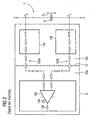
- FIG. 2 shows such a known driver 6 with primary side 10a and secondary side 10b, wherein the secondary side 10b has a TOP assembly 14a and a BOT assembly 14b.
- the intermediate circuit capacitor 8 is shown, at which the intermediate circuit voltage U Z to be measured drops.
- the potentials P O and P U between which the voltage U Z is applied via a respective chain of resistors 100a, guided b by the potentials P O and P U through the secondary side 10b in the primary side 10a, where a differential amplifier 102nd
- the electrical isolation between the primary side 10a and the secondary side 10b, indicated by the line 12, is therefore no real galvanic isolation since it is bridged by the respective resistor chains 100a, b.
- the voltage U Z is converted into a voltage U Z proportional or correlated with this analog signal 104, which is provided at an output 106 of the differential amplifier 102 for further processing.
- Object of the present invention is to realize an improved detection of the DC link voltage in a driver circuit for a power converter with DC link.
- the object is achieved by a driver circuit for a power converter, which has a DC link.
- the driver circuit has a primary side and a secondary side.
- the secondary side contains a measuring device for outputting a correlated with the intermediate circuit voltage first analog signal.
- the secondary also includes an A / D converter for converting the first analog signal to a digital value.
- the digital value thus also represents the measured DC link voltage.
- the driver circuit also contains a galvanically isolating transmission element which serves to transmit the digital value from the secondary to the primary side.
- the actual voltage measurement is performed by the measuring device on the secondary side of the driver.
- the A / D converter is carried out on the secondary side safe and reliable feasible conversion of the measured first analog signal into a digital value.
- the transmission of the digital value as a bit pattern via a signal transmitter, so the transmission element in the form of a galvanically separated data transmission is interference-proof, age-proof and correspondingly simple and inexpensive to carry out.
- Galvanically safe separating digital transmission elements are available in suitable dielectric strength.
- the digital value correlated with the intermediate circuit voltage is exactly available on the primary side and can be processed there in any way.
- the driver circuit has a true, complete galvanic isolation.
- the measuring device and / or the A / D converter can therefore be in one of the secondary side of the driver own, i. already be used without implementation of the inventive Swiss Stammsmesslicks used controller.
- a driver circuit according to the invention therefore virtually no overhead on components is necessary, since measuring device and / or A / D converter are already available unused in such driver circuits anyway.
- the transmission element is also already available in such a digital driver, since an error or status feedback from the secondary to the primary side already takes place via this or via the data path formed by it.
- the primary side may include a D / A converter for converting the digital value into a second analog signal. For further processing is then on the primary side in the usual Way an exactly correlated with the DC link voltage analog signal available.
- the measuring device may be a differential amplifier connected to the intermediate circuit voltage.
- the driver circuit can be designed to drive two power semiconductor switches connected in series to the intermediate circuit voltage.
- the secondary side then has two modules, namely a TOP and a BOT module, each of these modules each driving a power semiconductor switch.
- the measuring device that is to say, for example, the differential amplifier, can then preferably be arranged in the BOT module. This is the one at the lower potential (P U in Fig. 2 ) of the intermediate circuit voltage lying module.
- the construction of the measuring device eg of a measuring amplifier, is simpler at the low potential P U or in the BOT module than when it is placed in the TOP module.
- the measuring device can then be connected to the TOP module via a resistor chain. Since the BOT module is connected to the lower potential of the intermediate circuit voltage, a high-resistance connection to the high potential of the intermediate circuit voltage thus exists via the resistor chain.
- the measuring device in the TOP module, if this is desired, for example, because of installation space or design advantages.
- a corresponding connection via a resistor chain to the BOT module can then also be realized.
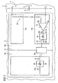
- Fig. 1 shows a section of a power converter 2, which includes an intermediate circuit 4 and a driver 6. From the intermediate circuit 4, only the intermediate circuit capacitor 8 is shown, on which the intermediate circuit voltage U Z is present as a DC voltage during operation of the power converter 2.
- the driver 6 has a primary side 10a and a secondary side 10b, which are galvanically separated from one another, indicated by the broken line 12.
- the secondary side 10b comprises a TOP module 14a and a BOT module 14b.
- the TOP module 14a in this case controls a power semiconductor switch, not shown, which is at the upper potential P O of the DC link 4.
- the BOT module 14b controls a second corresponding semiconductor switch, which lies on the lower potential P U of the DC link 4. Between the potentials P O and P U , the intermediate circuit voltage U Z prevails.
- the BOT module 14b contains a differential amplifier 16 whose measuring inputs 18a, b are connected to the potentials P O and P U.
- the measuring input 18a is directly connected through this.
- a resistor chain 20 Between the measuring input 18b and the potential P O or the TOP module 14b is a resistor chain 20.
- the differential amplifier 16 provides at its output 22, an analog signal 24, for example, proportional to the instantaneous value of the intermediate circuit voltage.
- the output 22 is connected to an input 26 of a controller 28 which fulfills various tasks, which are not explained in more detail in the driver 6, for example the control of the semiconductor switches (not shown) and the communication with the primary side 10a.
- a controller 28 which fulfills various tasks, which are not explained in more detail in the driver 6, for example the control of the semiconductor switches (not shown) and the communication with the primary side 10a.
- an A / D converter 30 is integrated, which is connected to the input 26, the analog signal 24 converts into a digital value 32 and this at the output 34 of the controller 28 is available.
- the digital value 32 is, for example, the digital value of the voltage U Z in volts.
- Primary side 10a and secondary side 10b are connected to a galvanically isolating signal transmitter 36 for digital communication.
- the signal transmitter 36 is connected to the controller 28 and to a controller 38, which is located on the primary side 10a.
- the controller 38 also assumes a number of tasks which are not explained in more detail in the driver 6, e.g. the provision of the to be transmitted to the secondary side 10b switching commands for the semiconductor switches, not shown.
- a D / A converter is integrated 40, which converts the data transmitted from signal transmitter 36 digital value 32 into an analog signal 24b, which corresponds to the effect on the analog signal 24a, it clearly Z is correlated with the intermediate circuit voltage U.
- the Analog signal 24b accordingly in the usual way, eg as in Fig. 2 be further processed.
- the digital value 32 can be processed further in the controller 38, which supplies the same information about the intermediate circuit voltage U Z as the analog signals 24a, b.
- the controllers 28 and 38 and the signal transformer 36 may also be present only specifically for voltage measurement of the intermediate circuit voltage U Z and otherwise fulfill no tasks.
Landscapes
- Engineering & Computer Science (AREA)
- Power Engineering (AREA)
- Arrangements For Transmission Of Measured Signals (AREA)
- Measurement Of Current Or Voltage (AREA)
- Inverter Devices (AREA)
- Electric Propulsion And Braking For Vehicles (AREA)
Applications Claiming Priority (1)
| Application Number | Priority Date | Filing Date | Title |
|---|---|---|---|
| DE102007036700A DE102007036700A1 (de) | 2007-08-03 | 2007-08-03 | Treiberschaltung für einen Stromrichter mit Zwischenkreis |
Publications (2)
| Publication Number | Publication Date |
|---|---|
| EP2020751A2 true EP2020751A2 (fr) | 2009-02-04 |
| EP2020751A3 EP2020751A3 (fr) | 2013-06-05 |
Family
ID=40001410
Family Applications (1)
| Application Number | Title | Priority Date | Filing Date |
|---|---|---|---|
| EP20080012362 Withdrawn EP2020751A3 (fr) | 2007-08-03 | 2008-07-09 | Circuit d'excitation pour un convertisseur de courant avec circuit intermédiaire |
Country Status (3)
| Country | Link |
|---|---|
| EP (1) | EP2020751A3 (fr) |
| CN (1) | CN101359874B (fr) |
| DE (1) | DE102007036700A1 (fr) |
Cited By (1)
| Publication number | Priority date | Publication date | Assignee | Title |
|---|---|---|---|---|
| WO2020104204A1 (fr) * | 2018-11-19 | 2020-05-28 | Bombardier Transportation Gmbh | Convertisseur de source de tension et son procédé de fonctionnement |
Families Citing this family (1)
| Publication number | Priority date | Publication date | Assignee | Title |
|---|---|---|---|---|
| DE102010038735B3 (de) * | 2010-07-30 | 2011-11-17 | Semikron Elektronik Gmbh & Co. Kg | Verfahren zum Betreiben eines PWM-Ausgangs eines Treibers für einen Leistungshalbleiter |
Citations (9)
| Publication number | Priority date | Publication date | Assignee | Title |
|---|---|---|---|---|
| DE2930767A1 (de) * | 1979-07-28 | 1981-02-19 | Bbc Brown Boveri & Cie | Einrichtung zur messung hoher gleichspannungen |
| DE3229750A1 (de) * | 1982-08-10 | 1984-02-16 | Siemens AG, 1000 Berlin und 8000 München | Ueberwachungseinheit fuer messwerte, insbesondere eines stromrichter-zwischenkreises |
| US4521672A (en) | 1981-10-27 | 1985-06-04 | Miller Electric Manufacturing Company | Electronic welding apparatus |
| EP0844729A2 (fr) | 1996-11-25 | 1998-05-27 | Asea Brown Boveri AG | Procédure et dispositif pour supprimer le décalage de tension continu |
| WO2002027913A1 (fr) * | 2000-09-29 | 2002-04-04 | Siemens Aktiengesellschaft | Commande d'entrainement pour un entrainement electrique presentant une isolation electrique fiable entre une partie de puissance et une unite de regulation |
| US20050253165A1 (en) | 2004-04-26 | 2005-11-17 | Gary Pace | Adaptive gate drive for switching devices of inverter |
| WO2005122423A2 (fr) * | 2004-06-03 | 2005-12-22 | Silicon Laboratories Inc. | Isolateur de spectre etale |
| US20060012382A1 (en) * | 2004-07-19 | 2006-01-19 | Fieldmetrics Inc | Modular voltage sensor |
| DE102005045957A1 (de) | 2005-09-26 | 2006-11-16 | Siemens Ag | Verfahren und Vorrichtung zur Übertragung von Signalen |
Family Cites Families (6)
| Publication number | Priority date | Publication date | Assignee | Title |
|---|---|---|---|---|
| CN1010730B (zh) * | 1985-09-25 | 1990-12-05 | 三菱电机株式会社 | 交换器的控制方法 |
| DE4006163C1 (en) * | 1990-02-24 | 1991-08-29 | Aeg Westinghouse Transport-Systeme Gmbh, 1000 Berlin, De | Protecting power electronics equipment - regulating intermediate circuit for constant voltage and operating short-circuiting protector upon overvoltage |
| JPH04322161A (ja) * | 1991-04-19 | 1992-11-12 | Nec Commun Syst Ltd | スイッチングレギュレータ制御方式 |
| US5689394A (en) * | 1995-12-04 | 1997-11-18 | General Electric Company | Gate voltage modulation for transistor fault conditions |
| DE19844980C2 (de) * | 1998-09-30 | 2000-10-26 | Siemens Ag | Meßvorrichtung zur Messung der Zwischenkreisspannung von Gradientenverstärkern |
| DE10048441A1 (de) * | 2000-09-29 | 2002-05-02 | Siemens Ag | Verfahren zur Erkennung von Spannungsüberschlägen in Ventilabschnitten mit einer Reihenschaltung von abschaltbaren Leistungshalbleitern sowie Ventilabschnitt einer derartigen Reihenschaltung |
-
2007
- 2007-08-03 DE DE102007036700A patent/DE102007036700A1/de not_active Withdrawn
-
2008
- 2008-07-09 EP EP20080012362 patent/EP2020751A3/fr not_active Withdrawn
- 2008-08-01 CN CN2008101450255A patent/CN101359874B/zh not_active Expired - Fee Related
Patent Citations (9)
| Publication number | Priority date | Publication date | Assignee | Title |
|---|---|---|---|---|
| DE2930767A1 (de) * | 1979-07-28 | 1981-02-19 | Bbc Brown Boveri & Cie | Einrichtung zur messung hoher gleichspannungen |
| US4521672A (en) | 1981-10-27 | 1985-06-04 | Miller Electric Manufacturing Company | Electronic welding apparatus |
| DE3229750A1 (de) * | 1982-08-10 | 1984-02-16 | Siemens AG, 1000 Berlin und 8000 München | Ueberwachungseinheit fuer messwerte, insbesondere eines stromrichter-zwischenkreises |
| EP0844729A2 (fr) | 1996-11-25 | 1998-05-27 | Asea Brown Boveri AG | Procédure et dispositif pour supprimer le décalage de tension continu |
| WO2002027913A1 (fr) * | 2000-09-29 | 2002-04-04 | Siemens Aktiengesellschaft | Commande d'entrainement pour un entrainement electrique presentant une isolation electrique fiable entre une partie de puissance et une unite de regulation |
| US20050253165A1 (en) | 2004-04-26 | 2005-11-17 | Gary Pace | Adaptive gate drive for switching devices of inverter |
| WO2005122423A2 (fr) * | 2004-06-03 | 2005-12-22 | Silicon Laboratories Inc. | Isolateur de spectre etale |
| US20060012382A1 (en) * | 2004-07-19 | 2006-01-19 | Fieldmetrics Inc | Modular voltage sensor |
| DE102005045957A1 (de) | 2005-09-26 | 2006-11-16 | Siemens Ag | Verfahren und Vorrichtung zur Übertragung von Signalen |
Cited By (2)
| Publication number | Priority date | Publication date | Assignee | Title |
|---|---|---|---|---|
| WO2020104204A1 (fr) * | 2018-11-19 | 2020-05-28 | Bombardier Transportation Gmbh | Convertisseur de source de tension et son procédé de fonctionnement |
| US11929685B2 (en) | 2018-11-19 | 2024-03-12 | Bombardier Transportation Gmbh | Voltage source converter and a method for operation thereof |
Also Published As
| Publication number | Publication date |
|---|---|
| EP2020751A3 (fr) | 2013-06-05 |
| CN101359874A (zh) | 2009-02-04 |
| DE102007036700A1 (de) | 2009-02-05 |
| CN101359874B (zh) | 2013-05-29 |
Similar Documents
| Publication | Publication Date | Title |
|---|---|---|
| EP2980659B1 (fr) | Dispositif et procédé destinés à la surveillance et la commutation d'un circuit de charge | |
| EP2002413B1 (fr) | Canal de transmission bidirectionnel séparé galvaniquement | |
| EP2980660B1 (fr) | Procédé et dispositif de surveillance et de commutation d'un circuit de charge | |
| EP3544166B1 (fr) | Alimentation électrique secondaire pour une alimentation électrique | |
| EP0413938A1 (fr) | Circuit pour surveiller l'état de commutation d'un transistor de puissance | |
| EP2498270A1 (fr) | Relais de sécurité et système de communication orienté vers la sécurité | |
| EP0543037B1 (fr) | Circuit de sortie intégré et paramétrable dans un circuit intégré | |
| EP1364459B1 (fr) | Dispositif de commutation de securite | |
| EP3308179A1 (fr) | Dispositif de commutation, dispositif de test et procédé pour faire fonctionner un dispositif de commutation pour un appareil de mesure pour un transformateur | |
| DE102016214263A1 (de) | Trennverstärker | |
| EP2555003B1 (fr) | Transducteur de courant et sectionneur de charge étant équipé avec celui-ci | |
| DE102007036700A1 (de) | Treiberschaltung für einen Stromrichter mit Zwischenkreis | |
| DE19758101A1 (de) | Elektronische Einrichtung zur Fehlerdiagnose von elektrischen Systemen | |
| WO2016139263A1 (fr) | Procédé et dispositif de détermination d'un courant de charge | |
| WO2019134806A1 (fr) | Commande de sécurité ayant au moins un contact de commutation semi-conducteur | |
| EP3489696A1 (fr) | Dispositif de mesure de courant, gamme de dispositifs de mesure de courant et procédé de mesure de courant | |
| CH682866A5 (de) | Hochspannungsschalter. | |
| EP1247109B1 (fr) | Circuit electrique pour convertir une grandeur d'entree electrique en une tension de sortie electrique | |
| EP1091332A1 (fr) | Instrument de mesure performant à deux double conducteurs | |
| EP0693722B1 (fr) | Régulateur de courant de cathode, en particulier pour un amplificateur de tube à onde progressive | |
| WO2014090319A1 (fr) | Transformateur de courant ainsi que sectionneur à coupure en charge équipé de ce transformateur de courant | |
| DE19847179B4 (de) | Schaltungsanordnung zum Erfassen einer galvanisch getrennten Spannung | |
| EP4686022A1 (fr) | Dispositif de sécurité électrique | |
| WO2024009230A1 (fr) | Procédé et circuit de régulation de courant | |
| EP0656639B1 (fr) | Entrée numérique pour station de détection |
Legal Events
| Date | Code | Title | Description |
|---|---|---|---|
| PUAI | Public reference made under article 153(3) epc to a published international application that has entered the european phase |
Free format text: ORIGINAL CODE: 0009012 |
|
| AK | Designated contracting states |
Kind code of ref document: A2 Designated state(s): AT BE BG CH CY CZ DE DK EE ES FI FR GB GR HR HU IE IS IT LI LT LU LV MC MT NL NO PL PT RO SE SI SK TR |
|
| AX | Request for extension of the european patent |
Extension state: AL BA MK RS |
|
| PUAL | Search report despatched |
Free format text: ORIGINAL CODE: 0009013 |
|
| AK | Designated contracting states |
Kind code of ref document: A3 Designated state(s): AT BE BG CH CY CZ DE DK EE ES FI FR GB GR HR HU IE IS IT LI LT LU LV MC MT NL NO PL PT RO SE SI SK TR |
|
| AX | Request for extension of the european patent |
Extension state: AL BA MK RS |
|
| RIC1 | Information provided on ipc code assigned before grant |
Ipc: H03K 17/567 20060101ALI20130502BHEP Ipc: H03K 17/691 20060101AFI20130502BHEP Ipc: H03K 17/689 20060101ALI20130502BHEP |
|
| 17P | Request for examination filed |
Effective date: 20131205 |
|
| AKX | Designation fees paid |
Designated state(s): AT BE BG CH CY CZ DE DK EE ES FI FR GB GR HR HU IE IS IT LI LT LU LV MC MT NL NO PL PT RO SE SI SK TR |
|
| 17Q | First examination report despatched |
Effective date: 20141124 |
|
| STAA | Information on the status of an ep patent application or granted ep patent |
Free format text: STATUS: THE APPLICATION HAS BEEN WITHDRAWN |
|
| 18W | Application withdrawn |
Effective date: 20151215 |