EP2022155B1 - Circuit de protection de charge/décharge, bloc d'éléments d'accumulateur intégrant le circuit de protection de charge/decharge, appareil électronique utilisant le bloc d'éléments - Google Patents
Circuit de protection de charge/décharge, bloc d'éléments d'accumulateur intégrant le circuit de protection de charge/decharge, appareil électronique utilisant le bloc d'éléments Download PDFInfo
- Publication number
- EP2022155B1 EP2022155B1 EP07743753A EP07743753A EP2022155B1 EP 2022155 B1 EP2022155 B1 EP 2022155B1 EP 07743753 A EP07743753 A EP 07743753A EP 07743753 A EP07743753 A EP 07743753A EP 2022155 B1 EP2022155 B1 EP 2022155B1
- Authority
- EP
- European Patent Office
- Prior art keywords
- discharge
- over
- charge
- circuit
- control fet
- Prior art date
- Legal status (The legal status is an assumption and is not a legal conclusion. Google has not performed a legal analysis and makes no representation as to the accuracy of the status listed.)
- Not-in-force
Links
Images


Classifications
-
- H—ELECTRICITY
- H02—GENERATION; CONVERSION OR DISTRIBUTION OF ELECTRIC POWER
- H02J—ELECTRIC POWER NETWORKS; CIRCUIT ARRANGEMENTS OR SYSTEMS FOR SUPPLYING OR DISTRIBUTING ELECTRIC POWER; SYSTEMS FOR STORING ELECTRIC ENERGY
- H02J7/00—Circuit arrangements for charging or discharging batteries or for supplying loads from batteries
- H02J7/60—Circuit arrangements for charging or discharging batteries or for supplying loads from batteries including safety or protection arrangements
- H02J7/663—Circuit arrangements for charging or discharging batteries or for supplying loads from batteries including safety or protection arrangements using battery or load disconnect circuits
-
- H—ELECTRICITY
- H01—ELECTRIC ELEMENTS
- H01M—PROCESSES OR MEANS, e.g. BATTERIES, FOR THE DIRECT CONVERSION OF CHEMICAL ENERGY INTO ELECTRICAL ENERGY
- H01M10/00—Secondary cells; Manufacture thereof
- H01M10/42—Methods or arrangements for servicing or maintenance of secondary cells or secondary half-cells
- H01M10/44—Methods for charging or discharging
-
- H—ELECTRICITY
- H01—ELECTRIC ELEMENTS
- H01M—PROCESSES OR MEANS, e.g. BATTERIES, FOR THE DIRECT CONVERSION OF CHEMICAL ENERGY INTO ELECTRICAL ENERGY
- H01M50/00—Constructional details or processes of manufacture of the non-active parts of electrochemical cells other than fuel cells, e.g. hybrid cells
- H01M50/20—Mountings; Secondary casings or frames; Racks, modules or packs; Suspension devices; Shock absorbers; Transport or carrying devices; Holders
- H01M50/202—Casings or frames around the primary casing of a single cell or a single battery
-
- Y—GENERAL TAGGING OF NEW TECHNOLOGICAL DEVELOPMENTS; GENERAL TAGGING OF CROSS-SECTIONAL TECHNOLOGIES SPANNING OVER SEVERAL SECTIONS OF THE IPC; TECHNICAL SUBJECTS COVERED BY FORMER USPC CROSS-REFERENCE ART COLLECTIONS [XRACs] AND DIGESTS
- Y02—TECHNOLOGIES OR APPLICATIONS FOR MITIGATION OR ADAPTATION AGAINST CLIMATE CHANGE
- Y02E—REDUCTION OF GREENHOUSE GAS [GHG] EMISSIONS, RELATED TO ENERGY GENERATION, TRANSMISSION OR DISTRIBUTION
- Y02E60/00—Enabling technologies; Technologies with a potential or indirect contribution to GHG emissions mitigation
- Y02E60/10—Energy storage using batteries
Definitions
- the present invention relates to a charge/discharge protection circuit of a lithium-ion secondary battery, for example, that is capable of reducing electric current consumption without increasing the chip size, preventing degradation of a discharge control FET, and reducing the battery charge time.
- the present invention also relates to a battery pack embedding such a charge/discharge protection circuit and various types of electronic apparatuses that use such a battery pack.
- Japanese Laid-Open Patent Publication No. 2002-176730 discloses a semiconductor device employed as a protection circuit of a battery pack as is shown in FIG. 5 .
- the illustrated semiconductor device (charge/discharge protection circuit) 1 as a main component of a battery pack A includes an overcharge detection circuit 11, an over-discharge detection circuit 12, a discharge over-current detection circuit 13, a short-circuit detection circuit 14, an oscillation circuit 16, a counter circuit 17, logic circuits 18, 20, a level shift circuit 19, a charge over-current detection circuit 21, delay circuits 24, 25, and a delay time reduction circuit 23.
- the overcharge detection circuit 11 When overcharge, over-discharge, discharge over-current, charge over-current, or short-circuit is detected by the overcharge detection circuit 11, the over-discharge detection circuit 12, the discharge over-current detection circuit 13, the charge over-current detection circuit 21, or the short-circuit detection circuit 14, the oscillation circuit 16 is activated and the counter circuit 17 starts counting operations.
- a Cout output is switched to low level "L” via the logic circuit (e.g., latch circuit) 18 and the level shift circuit 19 so that a charge control FET Q1 is turned off; and in the case of over-discharge, discharge over-current, or short-circuit detection, a Dout output is switched to low.level "L” via the logic circuit 20 so that a discharge control FET Q2 is turned off.
- the source voltage of the charge control FET Q1 becomes lower than the source voltage of the discharge control FET Q2. It is noted that the source voltage of the discharge control FET Q2 corresponds to the Vss terminal voltage of the semiconductor device 1, and although a resistance is connected to a V-terminal of the semiconductor device, since the V- terminal has high impedance, the source voltage of the charge control FET Q1 may be substantially equal to the V- terminal voltage of the semiconductor device 1.
- the above-described operations are basic operations performed by the charge/discharge protection circuit (semiconductor device) of FIG. 5 upon detecting overcharge, over-discharge, charge.over-current, discharge over-current, or short-circuit.
- the delay time set with respect to overcharge detection by the overcharge detection circuit 11 is at least 1 second so that a test time for testing the semiconductor device 1 may be relatively long.
- a TEST terminal when testing the semiconductor device 1 or a protection circuit substrate, a TEST terminal may be set to low level "L" so that the output frequency of the oscillation circuit 16 may be increased and the detection delay time may be decreased to enable reduction of the test time. It is noted that this scheme may also be applied to overcharge, over-discharge, or discharge over-current detection but is particularly advantageous when applied to overcharge detection that requires a relatively long delay time.
- the oscillation circuit 16 may be a ring oscillator that includes a constant current inverter and a condenser, for example. It is noted that the oscillation frequency of a ring oscillator is determined by a constant current value of a constant current source, a capacitor value, and a threshold value of the constant current inverter. Thus, a method for reducing the delay time may involve setting the signal of the test terminal to low level "L" to thereby (a) increase the constant current value of the constant current source; (b) substantially decrease the capacity value of a capacitor; or (c) change the threshold value of the constant current inverter of the ring oscillator, for example.
- the position at which the output of the counter circuit 17 is obtained may be changed to reduce the delay time instead of changing the oscillation frequency of the oscillation circuit 16, the details of which are described in Japanese Laid-Open Patent Publication No. 2002-176730 .
- recovery from over-discharge status to dischargeable status may be realized by establishing connection with a charger.
- a Vdd terminal voltage is less than or equal to an over-discharge detection voltage when a charger is connected
- a charge current is supplied via a parasitic diode of the discharge control FET Q2
- the output of terminal Dout may be set to high level "H” to turn on the discharge control FET Q2 and switch to dischargeable status.
- the Dout terminal may be immediately switched to high level "H".
- a PIN for recognizing charger connection or a comparator may be used to enable such charger connection recovery operations.
- the number of terminals has to be increased at the charger side as well as the IC side when the PIN is used, and in the case where the comparator is used, the chip size has to be increased so that current consumption may be increased.
- a charge/discharge protection circuit that is capable of controlling on/off operations of a discharge control FET using existing PINs and circuits, preventing the current consumption and the chip size from increasing, preventing degradation of the discharge control FET when a charger is connected, and reducing a battery charge time.
- a battery pack embedding such a charge/discharge protection circuit and an electronic apparatus using such a battery pack.
- a charge/discharge protection circuit that protects a secondary battery from overcharge, over-discharge, charge over-current, and discharge over-current is provided, the charge/discharge protection circuit including:
- a battery pack that includes a charge/discharge protection circuit according to an embodiment of the present invention.
- an electronic apparatus that includes a battery pack according to an embodiment of the present invention.
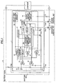
- FIG. 1 is a diagram showing a charge/discharge protection circuit (semiconductor device) according to an embodiment of the present invention.
- the illustrated charge/discharge protection circuit of FIG. 1 differs from the circuit shown in FIG. 5 in that it does not include a TEST terminal and includes a charger connection recovery circuit 26. It is noted that components of the charge/discharge protection circuit of the present embodiment that are identical to those shown in FIG. 5 are given the same reference numbers.
- the charge/discharge protection circuit 1 of the present embodiment includes an overcharge detection circuit 11, an over-discharge detection circuit 12, a discharge over-current detection circuit 13, a short-circuit detection circuit 14, an oscillation circuit 16, a counter circuit 17, logic circuits 18, 20, a level shift circuit 19, a charge over-current detection circuit 21, delay circuits 24, 25, a delay time reduction circuit 23, and the charger connection recovery circuit 26.
- the TEST terminal is not provided in the semiconductor device (charge/discharge detection circuit) 1 of FIG. 1 so that the number of terminals may be reduced compared to the semiconductor device 1 of FIG. 5 .
- a signal with a predetermined value e.g., -3 V
- the delay time reduction circuit 23 is applied to reduce the delay time in the manner described in relation to FIG. 5 (e.g., increasing the constant current value of the constant current source, substantially decreasing the capacity of the capacitor, or changing the threshold value of the constant current inverter).
- a charger connection signal corresponding to an internal circuit signal of the charge over-current detection circuit 21 a delay time reduction signal corresponding to an internal circuit signal of the delay time reduction circuit 23, an over-discharge detection signal corresponding to a detection signal from the over-discharge detection circuit 12, and an over-discharge confirmation signal that is inverted after the elapse of an over-discharge recovery delay time or an over-discharge detection delay time are used to control on/off operations of the discharge control FET Q2.
- the discharge control FET Q2 is forcefully turned on after the elapse of the over-discharge recovery delay time (first predetermined time) and then forcefully turned off after the elapse of the over-discharge detection delay time (second predetermined time). Further, in a case where a battery cell voltage is still less than or equal to an over-discharge detection voltage, the operations of turning on the discharge control FET Q2 after the elapse of the over-discharge recovery delay time and turning off the discharge control FET Q2 after the elapse of the over-discharge detection delay time are repeated.
- the over-discharge recovery delay time and the over-discharge detection delay time may be determined based on variations in internal circuit temperature characteristics, charger temperature characteristics, over-discharge recovery delay time temperature characteristics, and over-discharge detection delay time temperature characteristics, for example.
- the charger connection signal corresponding to an internal signal of the charge over-current detection circuit 21 is set to high level "H” when a charger is connected and is set to low level “L” when a charger is not connected.
- the delay time reduction signal corresponding to an internal signal of the delay time reduction circuit 23 is set to low level “L” when the delay time is being reduced and is set to high level “H” when the delay time is not reduced.
- the over-discharge detection signal corresponding to an internal signal of the over-discharge detection circuit (VD2) 12 is set to high level “H” when over-discharge is detected and is set to low level “L” when over-discharge is not detected.
- the over-discharge confirmation signal that is obtained from an internal signal of the over-discharge detection circuit (VD2) 12 is set to high level “H” after the elapse of the over-discharge detection delay time (second predetermined time: “tVdet2" of FIG. 4 ) from the time over-discharge is detected, and is set to low level “L” when over-discharge is not detected.
- FIG. 2A overcharge undetected, over-discharge undetected, over-current undetected, charger not connected
- the charge control FET Q1 and the discharge control FET Q2 are both turned on. In this case, the charger connection signal is at "L" level since the charger is not connected.
- the delay time reduction signal is at "H” level since operations are not in test mode (delay time reduction mode). Accordingly, "H" level and "L” level inputs are supplied to NAND gate M1 so that an "H" level output is obtained at M1.
- the over-discharge detection signal is at low level "L"
- the "H" level output of M1 and the over-discharge detection signal at "L” level are input to NAND gate M2 so that an "H" level output is obtained at M2.
- the "H” level output of M2 is input to inverter M3 so that an "L” level output is obtained at M3.
- the over-discharge detection confirmation signal is at low level “L” when over-discharge is not detected
- the "L" level output of M3 and the over-discharge detection confirmation signal at "L” level are input to EXNOR gate M4 so that an "H” level output is obtained at M4.
- the "H” level output of M4 is then input to a counter, and in this case, the counter is not activated.
- both the charge control FET Q1 and the discharge control FET Q2 are turned on.
- FIG. 2B over-discharge detected and charger not connected
- the over-discharge detection signal is at "H” level. Accordingly, the "H" level output of M1 and the over-discharge detection signal at "H” level are input to NAND gate M2 so that an "L” level output is obtained at M2.
- the “L” level output of M2 is input to inverter M3 so that an "H” level output is obtained at M3.
- the "H” level output of M3 and the over-discharge detection confirmation signal at “L” level are input to EXNOR gate M4 so that an "L” level output is obtained at M4.
- the “L” level output of M4 is input to the counter so that counting operations of the counter are activated. Then, after a predetermined time (over-discharge detection delay time) elapses from the time counting operations are started, the over-discharge detection confirmation signal is switched to "H” level. In turn, the output of M4 is switched to "H” level so that counting operations of the counter are stopped and the discharge control FET Q2 is turned off.
- the over-discharge detection confirmation signal may be inverted after the elapse of the predetermined time (over-discharge detection delay time) by inverting a flip flop that outputs the over-discharge detection confirmation signal at the time the counter counts to the predetermined time (over-discharge detection delay time).
- FIG. 2C over-discharge detected and charger connected
- the charger connection signal When over-discharge is detected and a charger is connected, the charger connection signal is set to “H” level and the delay time reduction signal is set to “H” level.
- the charger connection signal at "H” level and the delay time reduction signal at “H” level are input to NAND gate M1 so that an "L” level output is obtained at M1.
- the over-discharge detection signal is set to "H” level. Accordingly the “L” level output of M1 and the over-discharge detection signal at “H” level are input to NAND gate M2 so that an "H" level output is obtained at M2. The “H” level output of M2 is input to inverter M3 so that an "L” level output is obtained at M3.
- the over-discharge detection confirmation signal is set to "H” level. Accordingly, the "L" level output of M3 and the over-discharge detection confirmation signal at "H” level are input to EXNOR gate M4 so that an "L” level output is obtained at M4. The “L” level output of M4 is input to the counter so that counting operations of the counter are activated. Then, after a first predetermined time (over-discharge recovery delay time) elapses from the time counting operations are started, the discharge control FET Q2 may be forcefully turned on.
- a first predetermined time over-discharge recovery delay time
- the over-discharge detection confirmation signal may be inverted after the elapse of the first predetermined time (over-discharge recovery delay time) by inverting a flip flop that outputs the over-discharge detection confirmation signal at the time the counter counts to the first predetermined time (over-discharge recovery time).
- the discharge control FET Q2 is turned off after the elapse of the over-discharge detection delay time.
- the discharge control FET Q2 is forcefully turned on after the elapse of the over-discharge recovery delay time.
- pulse charge operations are performed by repeating the operations of turning off the discharge control FET Q2 after the elapse of the over-discharge detection delay time and turning on the discharge control FET Q2 after the elapse of the over-discharge recovery delay time.
- the pulse width of the charge pulse may be adjusted by changing the over-discharge detection delay time and the over-discharge recovery delay time according to variations in temperature characteristics of the internal circuits, the charger and the IC, for example.
- FIG. 4 is a timing chart illustrating charge operations performed when a charger is connected.
- the internal counter 17 counts to the over-discharge detection delay time (tVdet2) after which the output of Dout is switched to "L" level.
- the discharge control FET Q2 that is connected to Dout is turned off so that discharge operations are disabled.
- Vdet4 When the charger is connected under such conditions, the V- terminal temporarily falls to a charge over-current detection voltage (Vdet4) or lower.
- Vdet4 When the charge over-current (Vdet4) is detected, recovery from the over-discharge detection status to dischargeable status may be enabled by the charge over-current detection signal, the delay time reduction signal, the over-discharge detection signal, and the over-discharge detection confirmation signal, for example.
- the discharge control FET Q2 is turned on after the elapse of the over-discharge recovery delay time (tVrel2).
- the discharge control FET Q2 is turned off (Dout is switched to "L" level) after the elapse of the over-discharge detection delay time (tVdet2).
- pulse charge operations controlled by the over-discharge recovery delay time (tVrel2) and the over-discharge detection delay time (tVdet2) are performed until the level of Vdd rises above the over-discharge detection voltage.
- initial charge operations may be started in response to the connection of a charger. Then, the battery cell voltage may be checked by temporarily halting the charge operations (see “halt charge” of FIG. 4 ), and the charge operations may be resumed after the battery cell voltage is checked.
- Vdet2 the over-discharge detection voltage
- the discharge control FET Q2 that is turned off may be forcefully turned on after the elapse of a first predetermined time (over-discharge recovery delay time "tVrel2") so that the battery cell voltage may be monitored.
- a first predetermined time may be determined based on variations in internal circuit temperature characteristics, charger temperature characteristics, over-discharge recovery delay time temperature characteristics, and over-discharge detection delay time temperature characteristic, for example.
- a charge/discharge protection circuit according to an embodiment of the present invention may be embedded in a battery pack, and the battery pack may be installed in various types of electronic apparatuses such as a mobile phone, a portable game apparatus, a digital camera, or a portable audio apparatus.
- FIGS. 3A-3C are diagrams illustrating operations for controlling the discharge control FET Q2 under various conditions in the present example where such a charger connection detection terminal for detecting connection of a charger is used.
- FIG. 3A over-discharge undetected, charger not connected
- the charger connection signal may normally be at “L” level, and may be switched to "H” level when a signal from a battery pack positive (+) side of a charger is input and the charger is connected.
- a non-over-discharge detection signal that is set to "H” level when over-discharge is not detected and is set to "L” level when over-discharge is detected may be at "H” level.
- the charger connection signal is set to “L” level so that an "L” level output is obtained at NAND gate M1.
- the "L” level output of M1 is input to inverter M2 so that an "L” level output is obtained at M2.
- the discharge control FET Q2 corresponding to an N-channel FET may be turned on.
- FIG. 3B over-discharge detected and charger unconnected
- the non-over-discharge detection signal at "L” level is output, and when a charger is not connected, the charger connection signal at “L” level is output.
- the above “L” level outputs are input to NAND gate M1 so that an "H” level output may be obtained at M1.
- the “H” level output of M1 is input to inverter M2 so that an "L” level output may be obtained at M2.
- the discharge control FET Q2 is turned off.
- FIG. 3C over-discharge detected and charger connected
- a charge/discharge protection circuit with low current consumption and a relatively small chip size that is capable of preventing degradation of a discharge control FET when a charger is connected and reducing a battery charge time may be provided.
- a charge/discharge protection circuit even when a battery cell voltage is less than or equal to an over-discharge detection voltage so that the discharge control FET is turned off, the discharge control FET may be forcefully turned on when a charger is connected. It is noted that in a conventional charge/discharge protection circuit, when a charger is connected to perform charge operations at the time a discharge control FET is turned off, first, charge operations are performed using a parasitic diode of the discharge control FET. However, when such a parasitic diode is used in the charge operations, the discharge control FET may be prone to degradation.
- a charge/discharge protection circuit controls the discharge control FET to be forcefully turned on when a charger is connected at the time the discharge control FET is turned off to thereby prevent degradation of the discharge control FET and enable efficient charge operations in a short period of time, for example. Also, a charge/discharge protection circuit according to one preferred embodiment of the present invention does not have to include an additional terminal for detecting connection of a charger so that an increase in current consumption and chip size may be prevented, for example.
- the charge/discharge protection circuit according to an embodiment of the present invention may be embedded in a battery pack that is widely used in a variety of electronic apparatuses such as a mobile phone, a portable game apparatus, a digital camera, and a portable audio apparatus.
Landscapes
- Engineering & Computer Science (AREA)
- Chemical & Material Sciences (AREA)
- Chemical Kinetics & Catalysis (AREA)
- Electrochemistry (AREA)
- General Chemical & Material Sciences (AREA)
- Power Engineering (AREA)
- Manufacturing & Machinery (AREA)
- Charge And Discharge Circuits For Batteries Or The Like (AREA)
- Secondary Cells (AREA)
Abstract
Claims (10)
- Circuit de protection contre les charges/décharges qui protège une batterie secondaire d'une charge excessive, d'une décharge excessive, d'une surintensité de charge et d'une surintensité de décharge, ledit circuit de protection contre les charges/décharges comprenant :un circuit de détection de charge excessive (11) ;un circuit de détection de décharge excessive (12) ;un circuit de détection de surintensité de charge (21) ;un circuit de détection de surintensité de décharge (13) ;un transistor FET de commande de charge qui est bloqué lorsqu'une charge excessive est détectée par le circuit de détection de charge excessive et lorsqu'une surintensité de charge est détectée par le circuit de détection de surintensité de charge ; etun transistor FET de commande de décharge qui est bloqué lorsqu'une décharge excessive est détectée par le circuit de détection de décharge excessive et lorsqu'une surintensité de décharge est détectée par le circuit de détection de surintensité de décharge ; caractérisé parun circuit de récupération de connexion de chargeur (26) qui commande les opérations tout-ou-rien du transistor FET de commande de décharge de sorte que, lorsqu'une connexion avec un chargeur est établie à un instant où une décharge excessive est détectée et où le transistor FET de commande de décharge est bloqué, le transistor FET de commande de décharge soit rendu passant de force après qu'un premier temps prédéterminé s'est écoulé.
- Circuit de protection contre les charges/décharges selon la revendication 1, dans lequel le circuit de récupération de connexion de chargeur (20) est agencé pour bloquer le transistor FET de commande de décharge après qu'un deuxième temps prédéterminé s'est écoulé depuis l'instant où le transistor FET de commande de décharge a été rendu passant de force.
- Circuit de protection contre les charges/décharges selon la revendication 2, dans lequel le circuit de récupération de connexion de chargeur (26) est agencé pour répéter les opérations pour rendre passant le transistor FET de commande de décharge après que le premier temps prédéterminé s'est écoulé et pour bloquer le transistor FET de commande de décharge après que le deuxième temps prédéterminé s'est écoulé lorsqu'une tension de cellule de batterie est inférieure ou égale à une tension de détection de décharge excessive.
- Circuit de protection contre les charges/décharges selon la revendication 2, dans lequel
le premier temps prédéterminé et le deuxième temps prédéterminé sont déterminés en fonction de variations des caractéristiques de température des circuits internes, des caractéristiques de température du chargeur, des caractéristiques de température de temps de retard de récupération de décharge excessive, et des caractéristiques de température de temps de retard de détection de décharge excessive. - Bloc de batteries comprenant le circuit de protection contre les charges/décharges selon l'une quelconque des revendications 1 à 4.
- Appareil électronique comprenant le bloc de batteries selon la revendication 5.
- Téléphone mobile comprenant le bloc de batteries selon la revendication 5.
- Dispositif de jeu portable comprenant le bloc de batteries selon la revendication 5.
- Appareil photographique numérique comprenant le bloc de batteries selon la revendication 5.
- Appareil audio portable comprenant le bloc de batteries selon la revendication 5.
Applications Claiming Priority (2)
| Application Number | Priority Date | Filing Date | Title |
|---|---|---|---|
| JP2006153848A JP5020546B2 (ja) | 2006-06-01 | 2006-06-01 | 充放電保護回路、該充放電保護回路を組み込んだバッテリーパック、該バッテリーパックを用いた電子機器、携帯ゲーム機 |
| PCT/JP2007/060319 WO2007138901A1 (fr) | 2006-06-01 | 2007-05-15 | Circuit de protection de charge/décharge, bloc d'éléments d'accumulateur intégrant le circuit de protection de charge/decharge, appareil électronique utilisant le bloc d'éléments |
Publications (3)
| Publication Number | Publication Date |
|---|---|
| EP2022155A1 EP2022155A1 (fr) | 2009-02-11 |
| EP2022155A4 EP2022155A4 (fr) | 2010-05-05 |
| EP2022155B1 true EP2022155B1 (fr) | 2012-08-15 |
Family
ID=38778420
Family Applications (1)
| Application Number | Title | Priority Date | Filing Date |
|---|---|---|---|
| EP07743753A Not-in-force EP2022155B1 (fr) | 2006-06-01 | 2007-05-15 | Circuit de protection de charge/décharge, bloc d'éléments d'accumulateur intégrant le circuit de protection de charge/decharge, appareil électronique utilisant le bloc d'éléments |
Country Status (5)
| Country | Link |
|---|---|
| US (1) | US7772805B2 (fr) |
| EP (1) | EP2022155B1 (fr) |
| JP (1) | JP5020546B2 (fr) |
| KR (1) | KR100966871B1 (fr) |
| WO (1) | WO2007138901A1 (fr) |
Cited By (4)
| Publication number | Priority date | Publication date | Assignee | Title |
|---|---|---|---|---|
| DE102013007704A1 (de) | 2013-05-03 | 2014-11-06 | Volkswagen Aktiengesellschaft | Batterieschutz mittels aktivem Stromsensor |
| TWI469417B (zh) * | 2012-12-25 | 2015-01-11 | Energy Control Ltd | 具過充電安全電路的二次電池 |
| US9413177B2 (en) | 2014-11-05 | 2016-08-09 | Motorola Solutions, Inc. | Efficient apparatus and method for inhibiting corrosion with discharge blocking features in a battery |
| NL2035556B1 (en) * | 2023-08-04 | 2025-02-18 | Dpci Project 4 B V | Electronic pavement sign, computing system, computer program, method for charging a battery of an electronic pavement sign, and method for adjusting a brightness of an electronic pavement sign |
Families Citing this family (33)
| Publication number | Priority date | Publication date | Assignee | Title |
|---|---|---|---|---|
| JP4811181B2 (ja) * | 2006-08-01 | 2011-11-09 | 富士電機株式会社 | 二次電池保護装置 |
| CN101946383B (zh) * | 2008-03-13 | 2014-08-06 | 半导体元件工业有限责任公司 | 用于提供过电压保护的方法及其电路 |
| JP2009254215A (ja) * | 2008-04-10 | 2009-10-29 | Ricoh Co Ltd | 充電装置 |
| JP5212042B2 (ja) * | 2008-11-19 | 2013-06-19 | ミツミ電機株式会社 | 二次電池の過電流保護回路 |
| JP5439800B2 (ja) * | 2008-12-04 | 2014-03-12 | ミツミ電機株式会社 | 二次電池保護用集積回路装置及びこれを用いた二次電池保護モジュール並びに電池パック |
| JP5434168B2 (ja) | 2009-03-17 | 2014-03-05 | 株式会社リコー | 二次電池の保護用半導体装置およびそれを用いたバッテリパックならびに電子機器 |
| JP5544923B2 (ja) * | 2010-02-24 | 2014-07-09 | セイコーエプソン株式会社 | 保護回路および電子機器 |
| US9722334B2 (en) | 2010-04-07 | 2017-08-01 | Black & Decker Inc. | Power tool with light unit |
| JP2012023852A (ja) * | 2010-07-14 | 2012-02-02 | Renesas Electronics Corp | 過電流保護回路、及び半導体装置 |
| US8886152B2 (en) * | 2010-09-29 | 2014-11-11 | Qualcomm Incorporated | Emergency override of battery discharge protection |
| CN102545162B (zh) * | 2010-12-09 | 2014-06-04 | 无锡华润上华半导体有限公司 | 锂电池保护电路 |
| TW201237758A (en) * | 2011-03-15 | 2012-09-16 | Askey Computer Corp | Lithium cell simulating device |
| JP5679055B2 (ja) * | 2011-06-10 | 2015-03-04 | トヨタ自動車株式会社 | 電池の充電方法、及び電池の充電制御装置 |
| WO2014045745A1 (fr) * | 2012-09-18 | 2014-03-27 | Necエナジーデバイス株式会社 | Système de stockage d'énergie et procédé de protection de batterie |
| PH12016501486B1 (en) | 2014-01-28 | 2024-01-05 | Guangdong Oppo Mobile Telecommunications Corp Ltd | Terminal, power adapter and method for handling charging anomaly |
| CN103762691B (zh) * | 2014-01-28 | 2015-12-23 | 广东欧珀移动通信有限公司 | 电池充电装置及电池充电保护控制方法 |
| JP5888387B1 (ja) * | 2014-10-22 | 2016-03-22 | ミツミ電機株式会社 | 電池保護回路及び電池保護装置、並びに電池パック |
| JP6966864B2 (ja) * | 2017-04-20 | 2021-11-17 | エイブリック株式会社 | バッテリ装置 |
| USD929336S1 (en) | 2019-09-05 | 2021-08-31 | Techtronic Cordless Gp | Electrical interface |
| USD1013634S1 (en) | 2019-09-05 | 2024-02-06 | Techtronic Cordless Gp | Battery pack |
| USD929335S1 (en) | 2019-09-05 | 2021-08-31 | Techtronic Cordless Gp | Electrical interface |
| USD929337S1 (en) | 2019-09-05 | 2021-08-31 | Techtronic Cordless Gp | Electrical interface |
| USD953268S1 (en) | 2019-09-05 | 2022-05-31 | Techtronic Cordless Gp | Electrical interface |
| USD929334S1 (en) | 2019-09-05 | 2021-08-31 | Techtronic Cordless Gp | Electrical interface |
| USD929339S1 (en) | 2019-09-05 | 2021-08-31 | Techtronic Cordless Gp | Electrical interface |
| USD929338S1 (en) | 2019-09-05 | 2021-08-31 | Techtronic Cordless Gp | Electrical interface |
| JP7489907B2 (ja) * | 2020-12-03 | 2024-05-24 | エイブリック株式会社 | 充放電制御回路及びバッテリ装置 |
| CN114629192A (zh) * | 2020-12-10 | 2022-06-14 | 艾普凌科株式会社 | 屏蔽控制电路、控制器、充放电控制电路及电池装置 |
| CN113206305B (zh) * | 2021-04-13 | 2023-08-01 | 西安稳先半导体科技有限责任公司 | 一种电池保护装置、电池组件及终端 |
| CN113206306B (zh) * | 2021-04-13 | 2023-08-01 | 西安稳先半导体科技有限责任公司 | 一种电池保护装置、电池组件及终端 |
| CN113206304B (zh) * | 2021-04-13 | 2023-08-01 | 西安稳先半导体科技有限责任公司 | 一种电池保护装置、电池组件及终端 |
| TWI775542B (zh) * | 2021-07-26 | 2022-08-21 | 宏碁股份有限公司 | 避免意外關機之行動裝置及控制方法 |
| KR20230039565A (ko) * | 2021-09-14 | 2023-03-21 | 에이블릭 가부시키가이샤 | 셀 밸런스 회로, 셀 밸런스 장치, 충방전 제어 회로, 충방전 제어 장치 및 배터리 장치 |
Family Cites Families (17)
| Publication number | Priority date | Publication date | Assignee | Title |
|---|---|---|---|---|
| US5530336A (en) * | 1992-09-17 | 1996-06-25 | Sony Corporation | Battery protection circuit |
| JP3296385B2 (ja) * | 1994-07-06 | 2002-06-24 | ミツミ電機株式会社 | 電池の電圧検出回路 |
| US5789900A (en) * | 1994-12-05 | 1998-08-04 | Fuji Photo Film Co., Ltd. | Device for protecting a secondary battery from overcharge and overdischarge |
| JP3597617B2 (ja) * | 1995-12-27 | 2004-12-08 | 株式会社日立超エル・エス・アイ・システムズ | 二次電池保護回路 |
| JP3172095B2 (ja) * | 1996-06-14 | 2001-06-04 | セイコーインスツルメンツ株式会社 | 充放電制御回路と充電式電源装置 |
| JPH10112939A (ja) * | 1996-10-07 | 1998-04-28 | Nec Corp | 電源切替回路 |
| JP3195555B2 (ja) * | 1997-02-10 | 2001-08-06 | セイコーインスツルメンツ株式会社 | 充放電制御回路 |
| JPH10285810A (ja) * | 1997-04-07 | 1998-10-23 | Seiko Instr Inc | 充放電制御回路と充電式電源装置 |
| JPH11215716A (ja) * | 1998-01-20 | 1999-08-06 | Matsushita Electric Ind Co Ltd | 電池管理装置,電池パック及び電子機器 |
| US6313610B1 (en) * | 1999-08-20 | 2001-11-06 | Texas Instruments Incorporated | Battery protection circuit employing active regulation of charge and discharge devices |
| JP3498736B2 (ja) * | 2000-09-28 | 2004-02-16 | 株式会社リコー | 充放電保護回路、該充放電保護回路を組み込んだバッテリーパック、該バッテリーパックを用いた電子機器 |
| US6501248B2 (en) | 2000-09-28 | 2002-12-31 | Ricoh Company, Ltd. | Charge/discharge protection apparatus having a charge-state overcurrent detector, and battery pack including the same |
| JP3468220B2 (ja) * | 2000-12-26 | 2003-11-17 | 株式会社リコー | 充放電保護回路、および該充放電保護回路を組み込んだバッテリーパック、該バッテリーパックを用いた電子機器 |
| JP2002204532A (ja) * | 2001-01-05 | 2002-07-19 | Seiko Instruments Inc | バッテリー状態監視回路およびバッテリー装置 |
| JP3886389B2 (ja) | 2002-02-07 | 2007-02-28 | 株式会社リコー | 電池パック充電装置および充電方法 |
| JP3926699B2 (ja) | 2002-07-30 | 2007-06-06 | 株式会社リコー | 二次電池の充電装置及びその充電方法 |
| JP2004176730A (ja) * | 2002-11-22 | 2004-06-24 | Nsk Ltd | エンコーダ付車輪用転がり軸受ユニット |
-
2006
- 2006-06-01 JP JP2006153848A patent/JP5020546B2/ja active Active
-
2007
- 2007-05-15 US US11/996,937 patent/US7772805B2/en active Active
- 2007-05-15 EP EP07743753A patent/EP2022155B1/fr not_active Not-in-force
- 2007-05-15 WO PCT/JP2007/060319 patent/WO2007138901A1/fr not_active Ceased
- 2007-05-15 KR KR1020087002821A patent/KR100966871B1/ko not_active Expired - Fee Related
Cited By (6)
| Publication number | Priority date | Publication date | Assignee | Title |
|---|---|---|---|---|
| TWI469417B (zh) * | 2012-12-25 | 2015-01-11 | Energy Control Ltd | 具過充電安全電路的二次電池 |
| DE102013007704A1 (de) | 2013-05-03 | 2014-11-06 | Volkswagen Aktiengesellschaft | Batterieschutz mittels aktivem Stromsensor |
| DE102013007704B4 (de) | 2013-05-03 | 2023-06-01 | Volkswagen Aktiengesellschaft | Batterieschutz mittels aktivem Stromsensor |
| US9413177B2 (en) | 2014-11-05 | 2016-08-09 | Motorola Solutions, Inc. | Efficient apparatus and method for inhibiting corrosion with discharge blocking features in a battery |
| NL2035556B1 (en) * | 2023-08-04 | 2025-02-18 | Dpci Project 4 B V | Electronic pavement sign, computing system, computer program, method for charging a battery of an electronic pavement sign, and method for adjusting a brightness of an electronic pavement sign |
| WO2025032063A3 (fr) * | 2023-08-04 | 2025-03-20 | Dpci Project 4 B.V. | Panneau de chaussée électronique, système informatique, programme informatique, procédé de charge d'une batterie d'un panneau de chaussée électronique et procédé de réglage d'une luminosité d'un panneau de chaussée électronique |
Also Published As
| Publication number | Publication date |
|---|---|
| EP2022155A4 (fr) | 2010-05-05 |
| KR20080034141A (ko) | 2008-04-18 |
| US7772805B2 (en) | 2010-08-10 |
| US20090251104A1 (en) | 2009-10-08 |
| WO2007138901A1 (fr) | 2007-12-06 |
| JP5020546B2 (ja) | 2012-09-05 |
| EP2022155A1 (fr) | 2009-02-11 |
| JP2007325434A (ja) | 2007-12-13 |
| KR100966871B1 (ko) | 2010-06-29 |
Similar Documents
| Publication | Publication Date | Title |
|---|---|---|
| EP2022155B1 (fr) | Circuit de protection de charge/décharge, bloc d'éléments d'accumulateur intégrant le circuit de protection de charge/decharge, appareil électronique utilisant le bloc d'éléments | |
| CN101765957B (zh) | 充电/放电保护电路、包括充电/放电保护电路的电池组、及其电子设备 | |
| US10622819B2 (en) | Rechargeable battery protection integrated circuit, rechargeable battery protection device, and battery pack | |
| US6812673B2 (en) | Charge/discharge protection apparatus having a charge-state overcurrent detector, and battery pack including the same, and mobile electronic system | |
| US8179099B2 (en) | Battery state monitoring circuit and battery device | |
| US6768289B2 (en) | Charge/discharge protection circuit with latch circuit for protecting a charge control FET from overheating in a portable device | |
| US7816890B2 (en) | Semiconductor unit for protecting secondary battery, battery pack having the semiconductor unit built-in and electronic apparatus using it | |
| CN101465557B (zh) | 便携式设备、用于便携式设备的电池盒 | |
| US8581556B2 (en) | Protection circuit and battery pack having current varying circuit to vary current flowing through power terminal | |
| WO2008035523A1 (fr) | Générateur de tension de grille arrière, transistor à effet de champ quatre bornes à basculement par grille arrière, et circuit de protection de charge et décharge l'utilisant | |
| CN101752619A (zh) | 二次电池保护集成电路装置、二次电池保护模块和电池组 | |
| US8524385B2 (en) | Battery pack | |
| CN102055218A (zh) | 电池状态监视电路及电池装置 | |
| KR101422887B1 (ko) | 배터리 상태 감시 회로 및 배터리 장치 | |
| JP3948435B2 (ja) | 2次電池保護用icとそれを用いたバッテリパックおよび電子機器 | |
| KR101259657B1 (ko) | 반도체 장치 및 충전식 전원 장치 | |
| CN101453130A (zh) | 电池状态监视电路及电池装置 | |
| JP2009183050A (ja) | 電池パック |
Legal Events
| Date | Code | Title | Description |
|---|---|---|---|
| PUAI | Public reference made under article 153(3) epc to a published international application that has entered the european phase |
Free format text: ORIGINAL CODE: 0009012 |
|
| 17P | Request for examination filed |
Effective date: 20080128 |
|
| AK | Designated contracting states |
Kind code of ref document: A1 Designated state(s): AT BE BG CH CY CZ DE DK EE ES FI FR GB GR HU IE IS IT LI LT LU LV MC MT NL PL PT RO SE SI SK TR |
|
| AX | Request for extension of the european patent |
Extension state: AL BA HR MK RS |
|
| DAX | Request for extension of the european patent (deleted) | ||
| RBV | Designated contracting states (corrected) |
Designated state(s): DE FR GB |
|
| A4 | Supplementary search report drawn up and despatched |
Effective date: 20100407 |
|
| 17Q | First examination report despatched |
Effective date: 20100623 |
|
| GRAP | Despatch of communication of intention to grant a patent |
Free format text: ORIGINAL CODE: EPIDOSNIGR1 |
|
| RIC1 | Information provided on ipc code assigned before grant |
Ipc: H01M 10/44 20060101ALI20120127BHEP Ipc: H02J 7/00 20060101AFI20120127BHEP |
|
| GRAS | Grant fee paid |
Free format text: ORIGINAL CODE: EPIDOSNIGR3 |
|
| GRAA | (expected) grant |
Free format text: ORIGINAL CODE: 0009210 |
|
| AK | Designated contracting states |
Kind code of ref document: B1 Designated state(s): DE FR GB |
|
| REG | Reference to a national code |
Ref country code: GB Ref legal event code: FG4D |
|
| REG | Reference to a national code |
Ref country code: DE Ref legal event code: R096 Ref document number: 602007024792 Country of ref document: DE Effective date: 20121011 |
|
| PLBE | No opposition filed within time limit |
Free format text: ORIGINAL CODE: 0009261 |
|
| STAA | Information on the status of an ep patent application or granted ep patent |
Free format text: STATUS: NO OPPOSITION FILED WITHIN TIME LIMIT |
|
| 26N | No opposition filed |
Effective date: 20130516 |
|
| REG | Reference to a national code |
Ref country code: DE Ref legal event code: R097 Ref document number: 602007024792 Country of ref document: DE Effective date: 20130516 |
|
| PGFP | Annual fee paid to national office [announced via postgrant information from national office to epo] |
Ref country code: GB Payment date: 20140521 Year of fee payment: 8 |
|
| PGFP | Annual fee paid to national office [announced via postgrant information from national office to epo] |
Ref country code: DE Payment date: 20140521 Year of fee payment: 8 Ref country code: FR Payment date: 20140527 Year of fee payment: 8 |
|
| REG | Reference to a national code |
Ref country code: DE Ref legal event code: R082 Ref document number: 602007024792 Country of ref document: DE Representative=s name: SCHWABE SANDMAIR MARX, DE |
|
| REG | Reference to a national code |
Ref country code: GB Ref legal event code: 732E Free format text: REGISTERED BETWEEN 20150226 AND 20150304 |
|
| REG | Reference to a national code |
Ref country code: DE Ref legal event code: R081 Ref document number: 602007024792 Country of ref document: DE Owner name: RICOH ELECTRONIC DEVICES CO., LTD., IKEDA-CITY, JP Free format text: FORMER OWNER: RICOH COMPANY, LTD., TOKIO/TOKYO, JP Effective date: 20150306 Ref country code: DE Ref legal event code: R082 Ref document number: 602007024792 Country of ref document: DE Representative=s name: SCHWABE SANDMAIR MARX, DE Effective date: 20150306 Ref country code: DE Ref legal event code: R082 Ref document number: 602007024792 Country of ref document: DE Representative=s name: SCHWABE SANDMAIR MARX PATENTANWAELTE RECHTSANW, DE Effective date: 20150306 |
|
| REG | Reference to a national code |
Ref country code: FR Ref legal event code: TP Owner name: RICOH ELECTRONIC DEVICES CO., LTD, JP Effective date: 20150319 |
|
| REG | Reference to a national code |
Ref country code: DE Ref legal event code: R119 Ref document number: 602007024792 Country of ref document: DE |
|
| GBPC | Gb: european patent ceased through non-payment of renewal fee |
Effective date: 20150515 |
|
| REG | Reference to a national code |
Ref country code: FR Ref legal event code: ST Effective date: 20160129 |
|
| PG25 | Lapsed in a contracting state [announced via postgrant information from national office to epo] |
Ref country code: DE Free format text: LAPSE BECAUSE OF NON-PAYMENT OF DUE FEES Effective date: 20151201 Ref country code: GB Free format text: LAPSE BECAUSE OF NON-PAYMENT OF DUE FEES Effective date: 20150515 |
|
| PG25 | Lapsed in a contracting state [announced via postgrant information from national office to epo] |
Ref country code: FR Free format text: LAPSE BECAUSE OF NON-PAYMENT OF DUE FEES Effective date: 20150601 |