EP2023319A2 - Vorrichtung und Verfahren zur Ansteuerung einer Plasmaanzeigetafel - Google Patents
Vorrichtung und Verfahren zur Ansteuerung einer Plasmaanzeigetafel Download PDFInfo
- Publication number
- EP2023319A2 EP2023319A2 EP08252636A EP08252636A EP2023319A2 EP 2023319 A2 EP2023319 A2 EP 2023319A2 EP 08252636 A EP08252636 A EP 08252636A EP 08252636 A EP08252636 A EP 08252636A EP 2023319 A2 EP2023319 A2 EP 2023319A2
- Authority
- EP
- European Patent Office
- Prior art keywords
- pulses
- address
- electrodes
- sustain
- voltage level
- Prior art date
- Legal status (The legal status is an assumption and is not a legal conclusion. Google has not performed a legal analysis and makes no representation as to the accuracy of the status listed.)
- Withdrawn
Links
Images




Classifications
-
- G—PHYSICS
- G09—EDUCATION; CRYPTOGRAPHY; DISPLAY; ADVERTISING; SEALS
- G09G—ARRANGEMENTS OR CIRCUITS FOR CONTROL OF INDICATING DEVICES USING STATIC MEANS TO PRESENT VARIABLE INFORMATION
- G09G3/00—Control arrangements or circuits, of interest only in connection with visual indicators other than cathode-ray tubes
- G09G3/20—Control arrangements or circuits, of interest only in connection with visual indicators other than cathode-ray tubes for presentation of an assembly of a number of characters, e.g. a page, by composing the assembly by combination of individual elements arranged in a matrix no fixed position being assigned to or needed to be assigned to the individual characters or partial characters
- G09G3/22—Control arrangements or circuits, of interest only in connection with visual indicators other than cathode-ray tubes for presentation of an assembly of a number of characters, e.g. a page, by composing the assembly by combination of individual elements arranged in a matrix no fixed position being assigned to or needed to be assigned to the individual characters or partial characters using controlled light sources
- G09G3/28—Control arrangements or circuits, of interest only in connection with visual indicators other than cathode-ray tubes for presentation of an assembly of a number of characters, e.g. a page, by composing the assembly by combination of individual elements arranged in a matrix no fixed position being assigned to or needed to be assigned to the individual characters or partial characters using controlled light sources using luminous gas-discharge panels, e.g. plasma panels
- G09G3/288—Control arrangements or circuits, of interest only in connection with visual indicators other than cathode-ray tubes for presentation of an assembly of a number of characters, e.g. a page, by composing the assembly by combination of individual elements arranged in a matrix no fixed position being assigned to or needed to be assigned to the individual characters or partial characters using controlled light sources using luminous gas-discharge panels, e.g. plasma panels using AC panels
- G09G3/291—Control arrangements or circuits, of interest only in connection with visual indicators other than cathode-ray tubes for presentation of an assembly of a number of characters, e.g. a page, by composing the assembly by combination of individual elements arranged in a matrix no fixed position being assigned to or needed to be assigned to the individual characters or partial characters using controlled light sources using luminous gas-discharge panels, e.g. plasma panels using AC panels controlling the gas discharge to control a cell condition, e.g. by means of specific pulse shapes
- G09G3/294—Control arrangements or circuits, of interest only in connection with visual indicators other than cathode-ray tubes for presentation of an assembly of a number of characters, e.g. a page, by composing the assembly by combination of individual elements arranged in a matrix no fixed position being assigned to or needed to be assigned to the individual characters or partial characters using controlled light sources using luminous gas-discharge panels, e.g. plasma panels using AC panels controlling the gas discharge to control a cell condition, e.g. by means of specific pulse shapes for lighting or sustain discharge
-
- G—PHYSICS
- G09—EDUCATION; CRYPTOGRAPHY; DISPLAY; ADVERTISING; SEALS
- G09G—ARRANGEMENTS OR CIRCUITS FOR CONTROL OF INDICATING DEVICES USING STATIC MEANS TO PRESENT VARIABLE INFORMATION
- G09G3/00—Control arrangements or circuits, of interest only in connection with visual indicators other than cathode-ray tubes
- G09G3/20—Control arrangements or circuits, of interest only in connection with visual indicators other than cathode-ray tubes for presentation of an assembly of a number of characters, e.g. a page, by composing the assembly by combination of individual elements arranged in a matrix no fixed position being assigned to or needed to be assigned to the individual characters or partial characters
- G09G3/22—Control arrangements or circuits, of interest only in connection with visual indicators other than cathode-ray tubes for presentation of an assembly of a number of characters, e.g. a page, by composing the assembly by combination of individual elements arranged in a matrix no fixed position being assigned to or needed to be assigned to the individual characters or partial characters using controlled light sources
- G09G3/28—Control arrangements or circuits, of interest only in connection with visual indicators other than cathode-ray tubes for presentation of an assembly of a number of characters, e.g. a page, by composing the assembly by combination of individual elements arranged in a matrix no fixed position being assigned to or needed to be assigned to the individual characters or partial characters using controlled light sources using luminous gas-discharge panels, e.g. plasma panels
- G09G3/288—Control arrangements or circuits, of interest only in connection with visual indicators other than cathode-ray tubes for presentation of an assembly of a number of characters, e.g. a page, by composing the assembly by combination of individual elements arranged in a matrix no fixed position being assigned to or needed to be assigned to the individual characters or partial characters using controlled light sources using luminous gas-discharge panels, e.g. plasma panels using AC panels
- G09G3/291—Control arrangements or circuits, of interest only in connection with visual indicators other than cathode-ray tubes for presentation of an assembly of a number of characters, e.g. a page, by composing the assembly by combination of individual elements arranged in a matrix no fixed position being assigned to or needed to be assigned to the individual characters or partial characters using controlled light sources using luminous gas-discharge panels, e.g. plasma panels using AC panels controlling the gas discharge to control a cell condition, e.g. by means of specific pulse shapes
- G09G3/294—Control arrangements or circuits, of interest only in connection with visual indicators other than cathode-ray tubes for presentation of an assembly of a number of characters, e.g. a page, by composing the assembly by combination of individual elements arranged in a matrix no fixed position being assigned to or needed to be assigned to the individual characters or partial characters using controlled light sources using luminous gas-discharge panels, e.g. plasma panels using AC panels controlling the gas discharge to control a cell condition, e.g. by means of specific pulse shapes for lighting or sustain discharge
- G09G3/2942—Control arrangements or circuits, of interest only in connection with visual indicators other than cathode-ray tubes for presentation of an assembly of a number of characters, e.g. a page, by composing the assembly by combination of individual elements arranged in a matrix no fixed position being assigned to or needed to be assigned to the individual characters or partial characters using controlled light sources using luminous gas-discharge panels, e.g. plasma panels using AC panels controlling the gas discharge to control a cell condition, e.g. by means of specific pulse shapes for lighting or sustain discharge with special waveforms to increase luminous efficiency
-
- H—ELECTRICITY
- H01—ELECTRIC ELEMENTS
- H01B—CABLES; CONDUCTORS; INSULATORS; SELECTION OF MATERIALS FOR THEIR CONDUCTIVE, INSULATING OR DIELECTRIC PROPERTIES
- H01B3/00—Insulators or insulating bodies characterised by the insulating materials; Selection of materials for their insulating or dielectric properties
- H01B3/02—Insulators or insulating bodies characterised by the insulating materials; Selection of materials for their insulating or dielectric properties mainly consisting of inorganic substances
- H01B3/10—Insulators or insulating bodies characterised by the insulating materials; Selection of materials for their insulating or dielectric properties mainly consisting of inorganic substances metallic oxides
-
- H—ELECTRICITY
- H01—ELECTRIC ELEMENTS
- H01J—ELECTRIC DISCHARGE TUBES OR DISCHARGE LAMPS
- H01J11/00—Gas-filled discharge tubes with alternating current induction of the discharge, e.g. alternating current plasma display panels [AC-PDP]; Gas-filled discharge tubes without any main electrode inside the vessel; Gas-filled discharge tubes with at least one main electrode outside the vessel
- H01J11/20—Constructional details
- H01J11/34—Vessels, containers or parts thereof, e.g. substrates
- H01J11/40—Layers for protecting or enhancing the electron emission, e.g. MgO layers
-
- H—ELECTRICITY
- H01—ELECTRIC ELEMENTS
- H01J—ELECTRIC DISCHARGE TUBES OR DISCHARGE LAMPS
- H01J2211/00—Plasma display panels with alternate current induction of the discharge, e.g. AC-PDPs
- H01J2211/20—Constructional details
- H01J2211/34—Vessels, containers or parts thereof, e.g. substrates
- H01J2211/40—Layers for protecting or enhancing the electron emission, e.g. MgO layers
Definitions
- Embodiment examples relate to an apparatus and methods for driving a plasma display panel (PDP). More particularly, example embodiments relate to an apparatus having a PDP with a protective layer of relative high secondary electron emission capacity and relative short discharge delay time and methods for driving the same.
- PDP plasma display panel
- Plasma display panels have attracted considerable attention due to their characteristics of being large-size displays.
- panel resolution is increased in order to realize an ultrahigh resolution PDP, pixel size decreases. Accordingly, a number of charged particles in the discharge cells may also decrease, such that a higher driving voltage may be required to maintain a desirable level of brightness. Thus, discharge efficiency may be lowered.
- a protective layer in discharge cells of the PDP may be formed of a material having a high capacity for secondary electron emission, a short discharge delay time, and little temperature dependency. Large secondary electron emission may lead to the formation of numerous charged particles in the discharge cells, which may not be maintained during an address waiting time. Accordingly, wall charges may be lost and a discharge failure may occur.
- Example embodiments are directed to an apparatus for driving a PDP and methods thereof, which substantially overcome one or more of the disadvantages of the related art.
- At least one of the above and other features of example embodiments may be realized by providing an apparatus for driving a plasma display panel that includes first and second substrates, X electrodes, Y electrodes, and A electrodes between the substrates, and a protective layer on a surface of at least one of the substrates and formed of a material including magnesium oxide and scandium, the apparatus including a first driver configured to generate sustain pulses and to apply the sustain pulses to at least one of the X electrodes and the Y electrodes, and a second driver configured to generate address pulses, also referred to as address short pulses herein, and to apply the address short pulses to the A electrodes in synchronization with the sustain pulses.
- a first driver configured to generate sustain pulses and to apply the sustain pulses to at least one of the X electrodes and the Y electrodes
- a second driver configured to generate address pulses, also referred to as address short pulses herein, and to apply the address short pulses to the A electrodes in synchronization with the sustain pulses.
- the protective layer is provided on an inwardly facing surface, that is a surface of the at least one substrate that faces the other one of the first and second substrates.
- the address short pulses may have a pulse width less than a pulse width of the sustain pulses.
- the width of the address short pulses may be less than half the width of the sustain pulses.
- a voltage level of the address short pulses may be lower than a voltage level of the sustain pulses, and the voltage level of the address short pulses may be lower than a voltage level of address pulses applied to the A electrodes during an address period. All or some of the address short pulses may be aligned with the sustain pulses. One or more of the address short pulses may not be aligned with the sustain pulses.
- a plurality of subfields may be sequentially arranged in one frame, and the address short pulses may be applied to at least one intermediate subfield of the plurality of subfields.
- a plurality of subfields may be sequentially arranged in one frame, the subfields may each include an address period and a sustain period, scan pulses may be sequentially applied to the Y electrodes during the address period, and further address pulses synchronized with the scan pulses may be applied to A electrodes corresponding to discharge cells to be displayed, and the address short pulses may be applied during the sustain period.
- First sustain pulses having a positive voltage level and second sustain pulses having a negative voltage level may be alternately applied to the Y electrodes during the sustain period, and the address short pulses may include first address short pulses having a positive level applied in synchronization with the first sustain pulses, and second address short pulses having a negative level applied in synchronization with the second sustain pulses:
- the protective layer material may further include one or more of aluminum, calcium, or zirconium.
- At least one of the above and other features of example embodiments may also be realized by providing a method of driving a plasma display panel that includes first and second substrates, X electrodes, Y electrodes, and A electrodes between the substrates, and a protective layer on a surface of at least one of the substrates and formed of a material including magnesium oxide and scandium, the method including generating sustain pulses, applying the sustain pulses to at least one of the X electrodes and the Y electrodes, generating address pulses, also referred to as address short pulses herein, and applying the address short pulses to the A electrodes in synchronization with the sustain pulses.
- the address short pulses may have a pulse width less than a pulse width of the sustain pulses.
- the width of the address short pulses may be less than half the width of the sustain pulses.
- a voltage level of the address short pulses may be lower than a voltage level of the sustain pulses, and the voltage level of the address short pulses may be lower than a voltage level of address pulses applied to the A electrodes during an address period. All or some of the address short pulses may be aligned with the sustain pulses. One or more of the address short pulses may not be aligned with the sustain pulses.
- a plurality of subfields may be arranged sequentially in one frame, and the address short pulses may be applied to at least one intermediate subfield of the plurality of subfields.
- a plurality of subfields may be sequentially arranged in one frame, the subfields may each include an address period and a sustain period, scan pulses may be sequentially applied to the Y electrodes during the address period, and further address pulses synchronized with the scan pulses may be applied to A electrodes corresponding to discharge cells to be displayed, and the address short pulses may be applied during the sustain period.
- First sustain pulses having a positive voltage level and second sustain pulses having a negative voltage level may be alternately applied to the Y electrodes during the sustain period, and the address short pulses may include first address short pulses having a positive level applied in synchronization with the first sustain pulses, and second address short pulses having a negative level applied in synchronization with the second sustain pulses.
- the protective layer material may further include one or more of aluminum, calcium, or zirconium.
- FIG. 1 illustrates an exploded perspective view of a PDP according to an example embodiment
- FIG. 2 illustrates a block diagram of an apparatus for driving the PDP according to an example embodiment
- FIG. 3 illustrates a timing diagram of driving signals output from drivers of the PDP of FIG. 2 according to an example embodiment
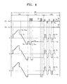
- FIG. 4 illustrates a timing diagram of driving signals output from the drivers of the PDP of FIG. 2 according to another example embodiment
- FIG. 5 illustrates a timing diagram of driving signals output from drivers of the PDP of FIG. 2 showing address short pulses applied in synchronization with only some of sustain pulses applied to the Y electrodes.
- FIG. 6 illustrates a timing diagram of driving signals output from drivers of the PDP of FIG. 2 showing a frame having a plurality of subfields in only some of which address short pulses are applied.
- a PDP 1 may include a first substrate 10 and a second substrate 13, each having an inner surface and an outer surface. The inner surfaces of the first substrate 10 and the second substrate 13 face one another.
- the PDP 1 may include a plurality of electrodes, e.g., A electrodes, Y electrodes, and X electrodes.
- the A electrodes include electrodes A R1 through A Bm
- the Y electrodes include electrodes Y 1 through Y n
- the X electrodes may include electrodes X 1 through X n .
- the PDP 1 further includes a first dielectric layer 11, a second dielectric layer 15, a phosphor layer 16, barrier ribs 17, and a protective layer 12.
- the A electrodes A R1 through A Bm maybe arranged in a pattern on the inner surface of the second substrate 13 and may be arranged in a first direction.
- the second dielectric layer 15 may overlay and/or bury portions of the A electrodes A R1 through A Bm .
- the barrier ribs 17 may be arranged parallel to the A electrodes A R1 through A Bm on a top surface of the second dielectric layer 15.
- the barrier ribs 17 may partition discharge areas of discharge cells 14 and may prevent optical cross-talk between the discharge cells 14.
- the phosphor layer 16 may be formed on sidewalls of the barrier ribs 17 and/or on a top surface of the second dielectric layer 15.
- the X electrodes X 1 through X n and the Y electrodes Y 1 and Y n may be arranged in a pattern on the inner surface of the first substrate 10 and may be arranged in a second direction approximately perpendicular to the first direction, so that portions of the X and Y electrodes may intersect the A electrodes A R1 through A Bm .
- the discharge cells 14 may be formed at crossings between the X electrodes X 1 through X n and Y electrodes Y 1 and Y n and the A electrodes A R1 through A Bm .
- Each of the X electrodes X 1 through X n and each of the Y electrodes Y 1 through Y n may be formed by coupling a transparent conductive electrode formed of a material, e.g., indium tin oxide (ITO), with a metal electrode to increase electrical conductivity.
- ITO indium tin oxide
- the X electrodes X 1 through X n may act as sustain electrodes
- the Y electrodes Y 1 through Y n may act as scan electrodes
- the A electrodes A R1 through A Bm may act as address electrodes.
- the first substrate 10 and the second substrate 13 may be formed of a transparent material, e.g., glass.
- the protective layer 12 may be formed of one or more materials including a rare earth metal.
- the protective layer 12 may include magnesium oxide (MgO) and scandium (Sc).
- the protective layer 12 may include one or more of: MgO and Sc; MgO, Sc and aluminum (Al); MgO, Sc, Al and calcium (Ca); and MgO, Sc, and zirconium (Zr).
- the protective layer 12 may exhibit little or no temperature dependency, may have a relatively high secondary electron emission capacity, and may provide a relatively short discharge delay time.
- the Y electrodes Y 1 through Y n may receive sequential scan pulses for selected discharge cells.
- the X electrodes X 1 through X n operate as sustain electrodes
- the X electrodes X l through X n may cause a sustain discharge between the X electrodes X 1 through X n and the Y electrodes Y 1 through Y n .
- an apparatus 20 for driving the PDP 1 may include an image processor 21, a logic controller 22, an A electrode driver 23, an X electrode driver 24, and a Y electrode driver 25.
- the image processor 21 may convert external analog image signals into digital signals and may generate internal image signals, e.g., red (R), green (G), and blue (B) image signals, a clock signal, and vertical and horizontal sync signals, each with 8 bits.
- the logic controller 22 may receive the internal image signals from the image processor 21 and may output driving control signals S A , S Y , and S X .
- the A electrode driver 23, the X electrode driver 24, and the Y electrode driver 25 may receive the respective driving control signals S A , S Y , and S X .
- the A electrode driver 23, the X electrode driver 24, and the Y electrode driver 25 may then generate driving signals and may apply the generated driving signals to the corresponding A, X, and Y electrodes.
- the A electrode driver 23 may process the driving control signal S A , which may be an address signal, received from logic controller 22 to generate a display data signal, and may apply the generated display data signal to one or more of the A electrodes A Rl through A Bm .
- the X electrode driver 24 may process the driving control signal S X received from the logic controller 22 and may apply a display data signal to one or more of the X electrodes X 1 through X n .
- the Y electrode driver 25 may process the driving control signal S Y received from the logic controller 22 and may apply a display data signal to one or more of the Y electrodes Y 1 through Y n .
- the X electrode driver 24 and/or the Y electrode driver 25 may apply sustain pulses to cause a sustain discharge from at least one of the X electrodes X 1 through X n and the Y electrodes Y 1 through Y n .
- the A electrode driver 23 may apply address short pulses to the A electrodes A R1 through A Bm in synchronization with the sustain pulses.
- the address short pulses may be aligned with the sustain pulses, such that the address short pulses are applied simultaneously with the sustain pulses as shown in FIG. 3 .
- the address short pulses may be synchronized with the sustain pulses, and one or more of the address short pulses may be offset from the sustain pulses.
- the protective layer 12 may be formed with materials including MgO and Sc, large secondary electron emissions may be generated, which may lead to forming a surplus of charged particles in the discharge cells 14. Accordingly, an address discharge may fail to occur in subsequent subfields of a frame, thereby failing to cause a sustain discharge following the address discharge.
- the apparatus 20 may ensure that a sustain discharge occurs between the X electrodes X 1 through X n and the Y electrodes Y 1 through Y n by applying address short pulses to the A electrodes A R1 through A Bm during the sustain discharge.
- the address short pulses may have a pulse width less than the pulse width of the sustain pulses.
- the address short pulses may have a pulse width less than half the pulse width of the address pulses.
- the address short pulses may have a pulse width less than the pulse width of the sustain pulses.
- FIG. 3 illustrates a timing diagram of driving signals output from the drivers of the apparatus 20 of FIG. 2 according to an example embodiment. It is noted, however, that example embodiments are not limited to the driving signals illustrated in FIG. 3 , and driving signals different from those shown in FIG. 3 may be output from the drivers of FIG. 2 in other example embodiments.
- a unit frame for driving the PDP 1 may be divided into a plurality of subfields SF, and the subfields SF may be divided into a reset period PR, an address period PA, and a sustain period PS.
- reset pulses including a rising pulse and a falling pulse may be applied to the Y electrodes Y 1 through Y n
- a second voltage e.g., a bias voltage
- the second voltage may be applied to the X electrodes X 1 through X n when the falling pulse is applied to the Y electrodes Y 1 through Y n , so as to perform a reset discharge.
- the discharge cells 14 may be initialized in response to the reset discharge.
- the rising pulse in the reset period PR may rise from a sustain discharge voltage V s by raising voltage V set to a rising maximum voltage V s + V set .
- the falling pulse in the reset period PR may fall from the sustain discharge voltage V s to a falling minimum voltage V nf .
- scan pulses may be sequentially applied to the Y electrodes Y 1 through Y n
- display data signals may be applied to the A electrodes A R1 through A Bm in synchronization with the scan pulses to perform an address discharge.
- the scan pulses may include a sequential scan high voltage V sch and a scan low voltage V scl lower than the scan high voltage V sch .
- the display data signals may have a positive address voltage V a in synchronization with the scan pulses with the scan low voltage V scl .
- sustain pulses may be alternately applied to the X electrodes X 1 through X n and the Y electrodes Y 1 through Y n , to perform a sustain discharge.
- the sustain discharge may represent brightness according to gray scale weights assigned to the respective subfields SF.
- the sustain pulses may alternately have a sustain discharge voltage V s and a ground voltage V g .
- address short pulses synchronized with the sustain pulses may be applied to the A electrodes A R1 through A Bm . The address short pulses may be applied approximately in synchronization with the sustain pulses.
- the address short pulses may ensure that at least some negative wall charges accumulated around the X electrodes X 1 through X n and the Y electrodes Y l through Y n may be moved toward the A electrodes A R1 through A Bm .
- the discharge volume of the sustain discharge may be increased, which may improve discharge efficiency and brightness.
- wall charges resulting from secondary electron emissions may be reduced by applying a greater number of sustain pulses in one frame. Accordingly, the address short pulses may be applied during the sustain period of the rear subfields in the frame.
- the address short pulses may be applied during the sustain period of an intermediate subfield of a frame as shown FIG. 6 , which may result in stable discharge without a discharge failure in subsequent subfields.
- the address short pulses may be applied in synchronization with the sustain pulses during the sustain period of the sixth through eighth subfields.
- the address short pulses may be applied in synchronization with at least one of the sustain pulses applied in the corresponding subfields. That is, the address short pulses may not be applied with all the sustain pulses in the corresponding subfields, but may be applied with only some of the sustain pulses in the corresponding subfields.
- the address short pulses may be illustrated as being applied in synchronization with all the sustain pulses in the subfields, example embodiments are not limited thereto.
- the address short pulses may be applied in synchronization with only sustain pulses applied to the X electrodes X l through X n , or the address short pulses may be applied in synchronization with only sustain pulses applied to the Y electrodes Y 1 through Y n as shown FIG. 5 .
- the address short pulses may have a voltage level V as lower than the voltage level V s of the sustain pulses, and the voltage level V as may be lower than the voltage level V a of the address pulses. Accordingly, the address short pulses may not cause a main discharge, but may ensure a sustain discharge to occur between the X electrodes X 1 through X n and the Y electrodes Y 1 through Y n .
- a method of driving the PDP 1 varies from the method described with reference to FIG. 3 in that the X electrodes X 1 through X n may be maintained at the ground level voltage V g , and driving signals may be primarily applied to the Y electrodes Y 1 through Y n . Because the driving signals may be applied by a driving circuit in the Y electrode driver 25, a driving circuit in the X electrode driver 24 may be simplified.
- the X electrodes X 1 through X n may be maintained at the ground level voltage V g during the reset period PR, the address period PA, and the sustain period PS.
- first sustain pulses having a positive voltage level +V s and second sustain pulses having a negative voltage level -V s may be alternately applied to the Y electrodes Y 1 through Y n .
- the address short pulses may include the first address short pulses having the positive voltage level +V as applied in synchronization with the first sustain pulses and second address short pulses having the negative voltage level -V as applied in synchronization with the second sustain pulses.
- the address short pulses may be applied in synchronization to some of the selected sustain pulses.
- the first address short pulses may have the negative voltage level -V as
- the second address short pulses may have the positive voltage level +V as .
- Example embodiments relate to an apparatus and method for driving a PDP by applying address short pulses during a sustain discharge period to improve brightness and discharge efficiency.
Landscapes
- Engineering & Computer Science (AREA)
- Physics & Mathematics (AREA)
- Plasma & Fusion (AREA)
- Theoretical Computer Science (AREA)
- Computer Hardware Design (AREA)
- General Physics & Mathematics (AREA)
- Power Engineering (AREA)
- Chemical & Material Sciences (AREA)
- Ceramic Engineering (AREA)
- Inorganic Chemistry (AREA)
- Control Of Indicators Other Than Cathode Ray Tubes (AREA)
- Control Of Gas Discharge Display Tubes (AREA)
- Gas-Filled Discharge Tubes (AREA)
Applications Claiming Priority (1)
| Application Number | Priority Date | Filing Date | Title |
|---|---|---|---|
| KR1020070079164A KR100884801B1 (ko) | 2007-08-07 | 2007-08-07 | 디스플레이 패널의 구동장치 및 그 구동방법 |
Publications (1)
| Publication Number | Publication Date |
|---|---|
| EP2023319A2 true EP2023319A2 (de) | 2009-02-11 |
Family
ID=39877880
Family Applications (1)
| Application Number | Title | Priority Date | Filing Date |
|---|---|---|---|
| EP08252636A Withdrawn EP2023319A2 (de) | 2007-08-07 | 2008-08-06 | Vorrichtung und Verfahren zur Ansteuerung einer Plasmaanzeigetafel |
Country Status (5)
| Country | Link |
|---|---|
| US (1) | US20090040143A1 (de) |
| EP (1) | EP2023319A2 (de) |
| JP (1) | JP2009042728A (de) |
| KR (1) | KR100884801B1 (de) |
| CN (1) | CN101364375A (de) |
Families Citing this family (1)
| Publication number | Priority date | Publication date | Assignee | Title |
|---|---|---|---|---|
| CN102034658B (zh) * | 2010-11-30 | 2012-12-26 | 四川虹欧显示器件有限公司 | 一种消除pdp放电故障的装置及方法 |
Citations (1)
| Publication number | Priority date | Publication date | Assignee | Title |
|---|---|---|---|---|
| US6744218B2 (en) | 2002-04-18 | 2004-06-01 | Samsung Sdi Co., Ltd. | Method of driving a plasma display panel in which the width of display sustain pulse varies |
Family Cites Families (6)
| Publication number | Priority date | Publication date | Assignee | Title |
|---|---|---|---|---|
| KR20020033664A (ko) * | 2002-01-30 | 2002-05-07 | 태흥식 | 교류형 플라즈마 디스플레이의 휘도 및 발광 효율 증가를위한 구동 방법 및 구동 장치 |
| US20070281185A1 (en) * | 2004-07-14 | 2007-12-06 | Mitsubishi Materials Corporation | Mgo Vapor Deposition Material |
| JP2006207014A (ja) * | 2004-07-14 | 2006-08-10 | Mitsubishi Materials Corp | MgO蒸着材 |
| KR100647616B1 (ko) * | 2004-09-24 | 2006-11-23 | 삼성에스디아이 주식회사 | 플라즈마 디스플레이 패널의 구동방법 |
| US7569992B2 (en) * | 2005-01-05 | 2009-08-04 | Lg Electronics Inc. | Plasma display panel and manufacturing method thereof |
| KR100726659B1 (ko) * | 2005-01-21 | 2007-06-13 | 엘지전자 주식회사 | 플라즈마 디스플레이 패널과 그의 보호막 및 그 제조 방법 |
-
2007
- 2007-08-07 KR KR1020070079164A patent/KR100884801B1/ko not_active Expired - Fee Related
-
2008
- 2008-02-12 JP JP2008030851A patent/JP2009042728A/ja not_active Withdrawn
- 2008-08-04 US US12/222,156 patent/US20090040143A1/en not_active Abandoned
- 2008-08-06 EP EP08252636A patent/EP2023319A2/de not_active Withdrawn
- 2008-08-07 CN CNA2008101298205A patent/CN101364375A/zh active Pending
Patent Citations (1)
| Publication number | Priority date | Publication date | Assignee | Title |
|---|---|---|---|---|
| US6744218B2 (en) | 2002-04-18 | 2004-06-01 | Samsung Sdi Co., Ltd. | Method of driving a plasma display panel in which the width of display sustain pulse varies |
Also Published As
| Publication number | Publication date |
|---|---|
| KR100884801B1 (ko) | 2009-02-23 |
| US20090040143A1 (en) | 2009-02-12 |
| JP2009042728A (ja) | 2009-02-26 |
| CN101364375A (zh) | 2009-02-11 |
| KR20090014862A (ko) | 2009-02-11 |
Similar Documents
| Publication | Publication Date | Title |
|---|---|---|
| KR100825344B1 (ko) | 표시 디바이스 및 플라즈마 표시 장치 | |
| KR100784597B1 (ko) | 플라즈마 디스플레이 패널 및 플라즈마 디스플레이 장치 | |
| US20080316147A1 (en) | Methods for resetting and driving plasma display panels in which address electrode lines are electrically floated | |
| US20050093777A1 (en) | Panel driving apparatus | |
| US6995735B2 (en) | Drive method of AC type plasma display panel | |
| EP2023319A2 (de) | Vorrichtung und Verfahren zur Ansteuerung einer Plasmaanzeigetafel | |
| US20070046573A1 (en) | Driving method of plasma display panel (PDP) | |
| US7969387B2 (en) | Method for driving plasma display device | |
| US20070069983A1 (en) | Method and apparatus for driving plasma display panel and plasma display device driven using the method and apparatus | |
| US20050218805A1 (en) | Plasma display panel and plasma display | |
| US20040239589A1 (en) | Plasma display panel apparatus and drive method thereof | |
| KR100482023B1 (ko) | 플라즈마 디스플레이 패널과 그 구동 방법 | |
| KR100516640B1 (ko) | 플라즈마 디스플레이 패널 구동방법 | |
| EP1995714A2 (de) | Plasmaanzeige | |
| JP2005157364A (ja) | プラズマディスプレイパネルの駆動方法及び装置 | |
| US7786956B2 (en) | Plasma display device | |
| KR100603307B1 (ko) | 개선된 동작 시퀀스를 가진 방전 표시 장치 | |
| KR100680696B1 (ko) | 플라즈마 표시 패널 구동 방법 및 장치 | |
| KR100741108B1 (ko) | 디스플레이 패널의 구동장치 | |
| JP2012013966A (ja) | プラズマディスプレイ装置の駆動方法、プラズマディスプレイ装置およびプラズマディスプレイシステム | |
| WO2007105480A1 (ja) | プラズマディスプレイ装置 | |
| CN101110193A (zh) | 等离子显示器驱动方法及其装置 | |
| KR20070096588A (ko) | 플라즈마 디스플레이 패널의 구동방법 | |
| JP2007078945A (ja) | プラズマディスプレイパネルの駆動方法 | |
| KR20080024386A (ko) | 디스플레이 패널의 구동장치 |
Legal Events
| Date | Code | Title | Description |
|---|---|---|---|
| PUAI | Public reference made under article 153(3) epc to a published international application that has entered the european phase |
Free format text: ORIGINAL CODE: 0009012 |
|
| 17P | Request for examination filed |
Effective date: 20080812 |
|
| AK | Designated contracting states |
Kind code of ref document: A2 Designated state(s): AT BE BG CH CY CZ DE DK EE ES FI FR GB GR HR HU IE IS IT LI LT LU LV MC MT NL NO PL PT RO SE SI SK TR |
|
| AX | Request for extension of the european patent |
Extension state: AL BA MK RS |
|
| STAA | Information on the status of an ep patent application or granted ep patent |
Free format text: STATUS: THE APPLICATION HAS BEEN WITHDRAWN |
|
| 18W | Application withdrawn |
Effective date: 20091218 |