EP2023372B1 - Unité de lentille électrostatique - Google Patents
Unité de lentille électrostatique Download PDFInfo
- Publication number
- EP2023372B1 EP2023372B1 EP07114130A EP07114130A EP2023372B1 EP 2023372 B1 EP2023372 B1 EP 2023372B1 EP 07114130 A EP07114130 A EP 07114130A EP 07114130 A EP07114130 A EP 07114130A EP 2023372 B1 EP2023372 B1 EP 2023372B1
- Authority
- EP
- European Patent Office
- Prior art keywords
- sample
- unit according
- lens unit
- cantilever
- electrode
- Prior art date
- Legal status (The legal status is an assumption and is not a legal conclusion. Google has not performed a legal analysis and makes no representation as to the accuracy of the status listed.)
- Not-in-force
Links
- 239000000523 sample Substances 0.000 claims description 147
- 238000000926 separation method Methods 0.000 claims description 34
- 238000000034 method Methods 0.000 claims description 22
- 239000000758 substrate Substances 0.000 claims description 21
- 239000002245 particle Substances 0.000 claims description 18
- 239000000463 material Substances 0.000 claims description 14
- 229910052581 Si3N4 Inorganic materials 0.000 claims description 12
- 239000011810 insulating material Substances 0.000 claims description 12
- HQVNEWCFYHHQES-UHFFFAOYSA-N silicon nitride Chemical compound N12[Si]34N5[Si]62N3[Si]51N64 HQVNEWCFYHHQES-UHFFFAOYSA-N 0.000 claims description 12
- 238000012876 topography Methods 0.000 claims description 11
- 230000000979 retarding effect Effects 0.000 claims description 8
- 229910052710 silicon Inorganic materials 0.000 claims description 7
- 239000010703 silicon Substances 0.000 claims description 7
- 230000008859 change Effects 0.000 claims description 3
- 230000002093 peripheral effect Effects 0.000 claims description 2
- 239000010410 layer Substances 0.000 description 76
- VYPSYNLAJGMNEJ-UHFFFAOYSA-N Silicium dioxide Chemical compound O=[Si]=O VYPSYNLAJGMNEJ-UHFFFAOYSA-N 0.000 description 56
- 239000000377 silicon dioxide Substances 0.000 description 28
- 235000012239 silicon dioxide Nutrition 0.000 description 25
- 238000010894 electron beam technology Methods 0.000 description 22
- 238000009826 distribution Methods 0.000 description 19
- WFKWXMTUELFFGS-UHFFFAOYSA-N tungsten Chemical compound [W] WFKWXMTUELFFGS-UHFFFAOYSA-N 0.000 description 16
- 229910052721 tungsten Inorganic materials 0.000 description 16
- 239000010937 tungsten Substances 0.000 description 16
- 238000003384 imaging method Methods 0.000 description 11
- KRHYYFGTRYWZRS-UHFFFAOYSA-N Fluorane Chemical compound F KRHYYFGTRYWZRS-UHFFFAOYSA-N 0.000 description 10
- 229920002120 photoresistant polymer Polymers 0.000 description 10
- 230000004075 alteration Effects 0.000 description 8
- 238000004519 manufacturing process Methods 0.000 description 8
- 239000012528 membrane Substances 0.000 description 8
- 238000005530 etching Methods 0.000 description 7
- QTBSBXVTEAMEQO-UHFFFAOYSA-N Acetic acid Chemical compound CC(O)=O QTBSBXVTEAMEQO-UHFFFAOYSA-N 0.000 description 6
- XUIMIQQOPSSXEZ-UHFFFAOYSA-N Silicon Chemical compound [Si] XUIMIQQOPSSXEZ-UHFFFAOYSA-N 0.000 description 6
- 239000011248 coating agent Substances 0.000 description 6
- 238000000576 coating method Methods 0.000 description 6
- 230000000694 effects Effects 0.000 description 6
- 238000001755 magnetron sputter deposition Methods 0.000 description 6
- 230000003287 optical effect Effects 0.000 description 6
- 238000011144 upstream manufacturing Methods 0.000 description 6
- 239000004020 conductor Substances 0.000 description 5
- 230000005684 electric field Effects 0.000 description 5
- 150000002500 ions Chemical class 0.000 description 5
- KFZMGEQAYNKOFK-UHFFFAOYSA-N Isopropanol Chemical compound CC(C)O KFZMGEQAYNKOFK-UHFFFAOYSA-N 0.000 description 4
- KWYUFKZDYYNOTN-UHFFFAOYSA-M Potassium hydroxide Chemical compound [OH-].[K+] KWYUFKZDYYNOTN-UHFFFAOYSA-M 0.000 description 4
- PCHJSUWPFVWCPO-UHFFFAOYSA-N gold Chemical compound [Au] PCHJSUWPFVWCPO-UHFFFAOYSA-N 0.000 description 4
- 239000010931 gold Substances 0.000 description 4
- 229910052737 gold Inorganic materials 0.000 description 4
- 239000004065 semiconductor Substances 0.000 description 4
- QVGXLLKOCUKJST-UHFFFAOYSA-N atomic oxygen Chemical compound [O] QVGXLLKOCUKJST-UHFFFAOYSA-N 0.000 description 3
- 238000004364 calculation method Methods 0.000 description 3
- 238000000605 extraction Methods 0.000 description 3
- 239000000203 mixture Substances 0.000 description 3
- 238000000206 photolithography Methods 0.000 description 3
- 230000008569 process Effects 0.000 description 3
- CSCPPACGZOOCGX-UHFFFAOYSA-N Acetone Chemical compound CC(C)=O CSCPPACGZOOCGX-UHFFFAOYSA-N 0.000 description 2
- SECXISVLQFMRJM-UHFFFAOYSA-N N-Methylpyrrolidone Chemical compound CN1CCCC1=O SECXISVLQFMRJM-UHFFFAOYSA-N 0.000 description 2
- GRYLNZFGIOXLOG-UHFFFAOYSA-N Nitric acid Chemical compound O[N+]([O-])=O GRYLNZFGIOXLOG-UHFFFAOYSA-N 0.000 description 2
- NBIIXXVUZAFLBC-UHFFFAOYSA-N Phosphoric acid Chemical compound OP(O)(O)=O NBIIXXVUZAFLBC-UHFFFAOYSA-N 0.000 description 2
- 238000004630 atomic force microscopy Methods 0.000 description 2
- 239000003795 chemical substances by application Substances 0.000 description 2
- 230000001276 controlling effect Effects 0.000 description 2
- 230000000875 corresponding effect Effects 0.000 description 2
- 238000000151 deposition Methods 0.000 description 2
- 230000008021 deposition Effects 0.000 description 2
- 238000001514 detection method Methods 0.000 description 2
- 239000002355 dual-layer Substances 0.000 description 2
- 238000001803 electron scattering Methods 0.000 description 2
- 238000005421 electrostatic potential Methods 0.000 description 2
- YAGKRVSRTSUGEY-UHFFFAOYSA-N ferricyanide Chemical compound [Fe+3].N#[C-].N#[C-].N#[C-].N#[C-].N#[C-].N#[C-] YAGKRVSRTSUGEY-UHFFFAOYSA-N 0.000 description 2
- 230000006872 improvement Effects 0.000 description 2
- 238000010884 ion-beam technique Methods 0.000 description 2
- 238000001340 low-energy electron microscopy Methods 0.000 description 2
- 238000005259 measurement Methods 0.000 description 2
- 229910052751 metal Inorganic materials 0.000 description 2
- 239000002184 metal Substances 0.000 description 2
- 229910017604 nitric acid Inorganic materials 0.000 description 2
- 229910052760 oxygen Inorganic materials 0.000 description 2
- 239000001301 oxygen Substances 0.000 description 2
- 238000012545 processing Methods 0.000 description 2
- 239000011253 protective coating Substances 0.000 description 2
- 230000001681 protective effect Effects 0.000 description 2
- 239000011241 protective layer Substances 0.000 description 2
- 238000001039 wet etching Methods 0.000 description 2
- 239000004411 aluminium Substances 0.000 description 1
- 229910052782 aluminium Inorganic materials 0.000 description 1
- XAGFODPZIPBFFR-UHFFFAOYSA-N aluminium Chemical compound [Al] XAGFODPZIPBFFR-UHFFFAOYSA-N 0.000 description 1
- PNEYBMLMFCGWSK-UHFFFAOYSA-N aluminium oxide Inorganic materials [O-2].[O-2].[O-2].[Al+3].[Al+3] PNEYBMLMFCGWSK-UHFFFAOYSA-N 0.000 description 1
- 229910000147 aluminium phosphate Inorganic materials 0.000 description 1
- 229910003481 amorphous carbon Inorganic materials 0.000 description 1
- 238000013459 approach Methods 0.000 description 1
- 150000001540 azides Chemical class 0.000 description 1
- 230000008901 benefit Effects 0.000 description 1
- 230000005540 biological transmission Effects 0.000 description 1
- 239000003054 catalyst Substances 0.000 description 1
- 238000005229 chemical vapour deposition Methods 0.000 description 1
- 238000004590 computer program Methods 0.000 description 1
- 238000012937 correction Methods 0.000 description 1
- 230000002596 correlated effect Effects 0.000 description 1
- 229910052593 corundum Inorganic materials 0.000 description 1
- 239000013078 crystal Substances 0.000 description 1
- 238000000708 deep reactive-ion etching Methods 0.000 description 1
- 230000001419 dependent effect Effects 0.000 description 1
- 238000013461 design Methods 0.000 description 1
- 238000010586 diagram Methods 0.000 description 1
- 238000006073 displacement reaction Methods 0.000 description 1
- 238000002003 electron diffraction Methods 0.000 description 1
- 238000000313 electron-beam-induced deposition Methods 0.000 description 1
- 239000012776 electronic material Substances 0.000 description 1
- 230000005686 electrostatic field Effects 0.000 description 1
- 238000011156 evaluation Methods 0.000 description 1
- 238000002474 experimental method Methods 0.000 description 1
- 230000005669 field effect Effects 0.000 description 1
- 239000007789 gas Substances 0.000 description 1
- 239000011521 glass Substances 0.000 description 1
- 230000036039 immunity Effects 0.000 description 1
- 238000007689 inspection Methods 0.000 description 1
- 238000000004 low energy electron diffraction Methods 0.000 description 1
- 229910001092 metal group alloy Inorganic materials 0.000 description 1
- 238000001465 metallisation Methods 0.000 description 1
- 150000002739 metals Chemical class 0.000 description 1
- 238000000386 microscopy Methods 0.000 description 1
- 238000012986 modification Methods 0.000 description 1
- 230000004048 modification Effects 0.000 description 1
- 238000012544 monitoring process Methods 0.000 description 1
- 239000011368 organic material Substances 0.000 description 1
- 230000036961 partial effect Effects 0.000 description 1
- 238000003909 pattern recognition Methods 0.000 description 1
- -1 potassium ferricyanide Chemical compound 0.000 description 1
- 238000005086 pumping Methods 0.000 description 1
- 230000002829 reductive effect Effects 0.000 description 1
- 238000012827 research and development Methods 0.000 description 1
- 230000004044 response Effects 0.000 description 1
- 230000002441 reversible effect Effects 0.000 description 1
- 230000000630 rising effect Effects 0.000 description 1
- 229910052594 sapphire Inorganic materials 0.000 description 1
- 239000010980 sapphire Substances 0.000 description 1
- 238000004621 scanning probe microscopy Methods 0.000 description 1
- 238000004574 scanning tunneling microscopy Methods 0.000 description 1
- 238000012216 screening Methods 0.000 description 1
- 230000035945 sensitivity Effects 0.000 description 1
- 125000006850 spacer group Chemical group 0.000 description 1
- 230000003068 static effect Effects 0.000 description 1
- XLYOFNOQVPJJNP-UHFFFAOYSA-N water Substances O XLYOFNOQVPJJNP-UHFFFAOYSA-N 0.000 description 1
- 229910001845 yogo sapphire Inorganic materials 0.000 description 1
Images








Classifications
-
- H—ELECTRICITY
- H01—ELECTRIC ELEMENTS
- H01J—ELECTRIC DISCHARGE TUBES OR DISCHARGE LAMPS
- H01J37/00—Discharge tubes with provision for introducing objects or material to be exposed to the discharge, e.g. for the purpose of examination or processing thereof
- H01J37/02—Details
- H01J37/04—Arrangements of electrodes and associated parts for generating or controlling the discharge, e.g. electron-optical arrangement or ion-optical arrangement
- H01J37/10—Lenses
- H01J37/12—Lenses electrostatic
-
- G—PHYSICS
- G01—MEASURING; TESTING
- G01Q—SCANNING-PROBE TECHNIQUES OR APPARATUS; APPLICATIONS OF SCANNING-PROBE TECHNIQUES, e.g. SCANNING PROBE MICROSCOPY [SPM]
- G01Q30/00—Auxiliary means serving to assist or improve the scanning probe techniques or apparatus, e.g. display or data processing devices
- G01Q30/02—Non-SPM analysing devices, e.g. SEM [Scanning Electron Microscope], spectrometer or optical microscope
-
- G—PHYSICS
- G01—MEASURING; TESTING
- G01Q—SCANNING-PROBE TECHNIQUES OR APPARATUS; APPLICATIONS OF SCANNING-PROBE TECHNIQUES, e.g. SCANNING PROBE MICROSCOPY [SPM]
- G01Q70/00—General aspects of SPM probes, their manufacture or their related instrumentation, insofar as they are not specially adapted to a single SPM technique covered by group G01Q60/00
- G01Q70/08—Probe characteristics
- G01Q70/10—Shape or taper
-
- H—ELECTRICITY
- H01—ELECTRIC ELEMENTS
- H01J—ELECTRIC DISCHARGE TUBES OR DISCHARGE LAMPS
- H01J37/00—Discharge tubes with provision for introducing objects or material to be exposed to the discharge, e.g. for the purpose of examination or processing thereof
- H01J37/02—Details
- H01J37/21—Means for adjusting the focus
-
- H—ELECTRICITY
- H01—ELECTRIC ELEMENTS
- H01J—ELECTRIC DISCHARGE TUBES OR DISCHARGE LAMPS
- H01J37/00—Discharge tubes with provision for introducing objects or material to be exposed to the discharge, e.g. for the purpose of examination or processing thereof
- H01J37/26—Electron or ion microscopes; Electron or ion diffraction tubes
- H01J37/28—Electron or ion microscopes; Electron or ion diffraction tubes with scanning beams
-
- H—ELECTRICITY
- H01—ELECTRIC ELEMENTS
- H01J—ELECTRIC DISCHARGE TUBES OR DISCHARGE LAMPS
- H01J2237/00—Discharge tubes exposing object to beam, e.g. for analysis treatment, etching, imaging
- H01J2237/03—Mounting, supporting, spacing or insulating electrodes
-
- H—ELECTRICITY
- H01—ELECTRIC ELEMENTS
- H01J—ELECTRIC DISCHARGE TUBES OR DISCHARGE LAMPS
- H01J2237/00—Discharge tubes exposing object to beam, e.g. for analysis treatment, etching, imaging
- H01J2237/04—Means for controlling the discharge
- H01J2237/047—Changing particle velocity
- H01J2237/0475—Changing particle velocity decelerating
- H01J2237/04756—Changing particle velocity decelerating with electrostatic means
-
- H—ELECTRICITY
- H01—ELECTRIC ELEMENTS
- H01J—ELECTRIC DISCHARGE TUBES OR DISCHARGE LAMPS
- H01J2237/00—Discharge tubes exposing object to beam, e.g. for analysis treatment, etching, imaging
- H01J2237/04—Means for controlling the discharge
- H01J2237/049—Focusing means
- H01J2237/0492—Lens systems
- H01J2237/04924—Lens systems electrostatic
-
- H—ELECTRICITY
- H01—ELECTRIC ELEMENTS
- H01J—ELECTRIC DISCHARGE TUBES OR DISCHARGE LAMPS
- H01J2237/00—Discharge tubes exposing object to beam, e.g. for analysis treatment, etching, imaging
- H01J2237/10—Lenses
- H01J2237/12—Lenses electrostatic
- H01J2237/1205—Microlenses
-
- H—ELECTRICITY
- H01—ELECTRIC ELEMENTS
- H01J—ELECTRIC DISCHARGE TUBES OR DISCHARGE LAMPS
- H01J2237/00—Discharge tubes exposing object to beam, e.g. for analysis treatment, etching, imaging
- H01J2237/10—Lenses
- H01J2237/12—Lenses electrostatic
- H01J2237/121—Lenses electrostatic characterised by shape
-
- H—ELECTRICITY
- H01—ELECTRIC ELEMENTS
- H01J—ELECTRIC DISCHARGE TUBES OR DISCHARGE LAMPS
- H01J2237/00—Discharge tubes exposing object to beam, e.g. for analysis treatment, etching, imaging
- H01J2237/20—Positioning, supporting, modifying or maintaining the physical state of objects being observed or treated
- H01J2237/202—Movement
- H01J2237/20292—Means for position and/or orientation registration
-
- H—ELECTRICITY
- H01—ELECTRIC ELEMENTS
- H01J—ELECTRIC DISCHARGE TUBES OR DISCHARGE LAMPS
- H01J2237/00—Discharge tubes exposing object to beam, e.g. for analysis treatment, etching, imaging
- H01J2237/244—Detection characterized by the detecting means
-
- H—ELECTRICITY
- H01—ELECTRIC ELEMENTS
- H01J—ELECTRIC DISCHARGE TUBES OR DISCHARGE LAMPS
- H01J2237/00—Discharge tubes exposing object to beam, e.g. for analysis treatment, etching, imaging
- H01J2237/25—Tubes for localised analysis using electron or ion beams
- H01J2237/2505—Tubes for localised analysis using electron or ion beams characterised by their application
- H01J2237/2538—Low energy electron microscopy [LEEM]
- H01J2237/2544—Diffraction [LEED]
-
- H—ELECTRICITY
- H01—ELECTRIC ELEMENTS
- H01J—ELECTRIC DISCHARGE TUBES OR DISCHARGE LAMPS
- H01J2237/00—Discharge tubes exposing object to beam, e.g. for analysis treatment, etching, imaging
- H01J2237/25—Tubes for localised analysis using electron or ion beams
- H01J2237/2505—Tubes for localised analysis using electron or ion beams characterised by their application
- H01J2237/2583—Tubes for localised analysis using electron or ion beams characterised by their application using tunnel effects, e.g. STM, AFM
-
- H—ELECTRICITY
- H01—ELECTRIC ELEMENTS
- H01J—ELECTRIC DISCHARGE TUBES OR DISCHARGE LAMPS
- H01J2237/00—Discharge tubes exposing object to beam, e.g. for analysis treatment, etching, imaging
- H01J2237/26—Electron or ion microscopes
- H01J2237/28—Scanning microscopes
-
- H—ELECTRICITY
- H01—ELECTRIC ELEMENTS
- H01J—ELECTRIC DISCHARGE TUBES OR DISCHARGE LAMPS
- H01J2237/00—Discharge tubes exposing object to beam, e.g. for analysis treatment, etching, imaging
- H01J2237/26—Electron or ion microscopes
- H01J2237/28—Scanning microscopes
- H01J2237/2818—Scanning tunnelling microscopes
Definitions
- the present invention relates to an electrostatic lens unit for a charged particle beam system particularly, but not exclusively, a scanning electron microscope system.
- Scanning electron microscopes can be used in a variety of applications to obtain high-resolution (e.g. ⁇ 1 ⁇ m) images of a sample.
- an electron gun emits a primary electron beam in which electrons have a high energy, typically of the order of 1 or 10 keV.
- An electron optics system comprising an arrangement of lenses and deflectors focuses and scans the beam across the sample with a typical spot size of the order of 10 nm.
- the fine beam interacts with a small volume of the sample causing it to emit low-energy secondary electrons, along with other scattered electrons, which are collected by a detector.
- the number of electrons emitted by the sample depends on a number of factors including orientation of the surface and the atomic number of atoms interacting with the beam. Thus, an image of the surface of the sample can be obtained.
- high-energy electrons are used to generate secondary electrons.
- the energy of the primary electron beam is maintained or varied only to a small degree (e.g. by a factor of 2 to 5) before the beam strikes the sample.
- high-energy electrons i.e. ⁇ 1 keV
- using high-energy electrons can have disadvantages, such as causing the sample to charge up, which can impair image quality and/or altering the electronic properties of the sample, such as charge distribution, which can change the characteristics of the sample, for example by causing a shift in threshold voltage of a field effect transistor.
- image contrast becomes strongly dependent upon electronic band structure and crystal structure of the material surface. This can yield additional information which is useful for investigating, for instance, new catalysts and novel electronic materials.
- a cathode lens situated between the objective lens and the sample and which applies a retarding electric field can be used to reduce the energy of electrons in the primary electric field.
- the cathode lens is placed as close as possible to the sample (i.e. the "working distance" is reduced as much as possible) to minimise exposure of low-energy electrons to stray magnetic fields and to reduce aberration.
- US-A-5 789 748 describes an SEM having a micro-lens unit which includes a retarding electrode situated 100 ⁇ m from the sample and which reduces the energy of the primary beam from 10 keV to 100 eV.
- this arrangement suffers the drawback that the retarding electrode is attached to the sample surface using a spacer.
- EP-A-1 134 771 describes an electron source capable of operating at low beam energies, e.g. of a few electron-volts, and which could be positioned close to a sample.
- the electron optics of the system are somewhat primitive compared with commonly-used SEMs and so beam characteristics, e.g. beam width, can be inferior.
- WO-A-2007096505 (Article 54(3) EPC) describes an arrangement comprising a specimen holder, a mask having a through-hole between upper and lower faces of the mask for allowing charged particles to pass through the mask and onto the specimen holder and a near-field detection device for detecting a relative position between the mask and the specimen holder.
- the mask includes at least one electrode in the through-hole.
- WO-A-0067290 describes apparatus for surface inspection and processing of a wafer includes a microcolumn and an associated scanning probe microscope.
- the microcolumn and scanning probe microscope can be partially fabricated out of the same substrate.
- the present invention seeks to provide an improved electrostatic lens unit.
- an electrostatic lens unit for a charged particle beam system including a substrate having first and second opposite faces and a passage extending between first and second openings in the first and second faces respectively, first and second face electrode supported on the first and second faces respectively, and a surface probe cantilever, formed by a slot in the substrate extending between the first and second opposite faces, the cantilever supporting a tip for sensing sample separation when the sample is adjacent the second face, wherein the cantilever is laterally spaced from the passage, wherein the first and second face electrodes are arranged around the respective openings to the passage and arranged on and around the cantilever.
- the second face of the electrostatic lens unit can be controllably positioned close to a sample so as to reduce the working distance.
- the probe does not interfere with scanning since it is laterally offset from the electrodes.
- the lens unit can be used to retard a primary beam of charged particles and so the exposure of low-energy charged particles to stray magnetic fields can be minimised.
- the substrate may include an insulating sheet and may comprise first and second portions, wherein the first portion is thicker than the second portion.
- the first portion may have a thickness of at least 5 ⁇ m and the second insulating sheet portion may have a thickness no more than 5 ⁇ m.
- the first portion of the substrate may support the second insulating sheet portion around a peripheral edge.
- the first and second portions may share a layer of insulating material, for example which comprises silicon nitride.
- the first region may comprise another layer of material, such as silicon.
- the second region need not include the second layer of material.
- the substrate may be arranged to provide a cantilever extending from the first portion to the second portion
- the unit may comprise at least two electrodes supported on the second face arranged in a stack and around the openings to the passage.
- the unit may comprise third, fourth and fifth electrode supported on the second face and arranged in a stack and around the openings to the passage.
- the probe e.g. a functional part at which separation is sensed, such as a tip or an electrode
- the probe and the aperture may be spaced apart from the apertures so as not to obscure the aperture.
- the probe and the aperture may be spaced apart by at least 10 ⁇ m, at least 20 ⁇ m or at least 50 ⁇ m.
- the probe and the aperture may be spaced apart by at least 100 ⁇ m.
- the substrate may be planar and may be stepped.
- apparatus comprising the lens unit, a means for supporting a sample and means for positioning the holder.
- the apparatus may further comprise means for positioning the electrostatic unit relative to the sample holder.
- the apparatus may further comprise a laser arranged to direct light onto the unit and a detector arranged to detect light reflected off the lens unit.
- a charged particle beam system apparatus positioned downstream of an objective lens.
- a method of operating a charged particle beam system which includes an electrostatic lens unit comprising a substrate having first and second opposite faces and a passage extending between first and second openings in the first and second faces respectively, first and second face electrodes supported on the first and second faces respectively, and a surface probe cantilever formed by a slot in the substrate extending between the first and second opposite faces, the cantilever supporting a tip for sensing sample separation, wherein the first and second electrodes are arranged around the respective openings to the passage and arranged on and around the cantilever, the method comprising sensing separation between the lens unit and a sample, directing a charged particle beam through the lens unit onto the sample and controlling the electrostatic lens unit to influence the charge particle beam including grounding the first electrode and applying a retarding potential to the second electrode and the sample.
- the method may further comprise adjusting the separation between the lens unit and a sample while sensing the separation using the probe.
- the method may comprise determining topography of the sample using the probe prior to scanning the charged particle beam.
- the method may further comprise adjusting the separation between the lens unit and the sample and/or controlling the electrostatic lens unit so as to change focus in dependence upon said topography.
- the system 1 includes a housing 2 (usually referred to as the "column") connected to a high- or ultra-high vacuum pumping system (not shown).
- the column 2 houses a cold field emission source 3 comprising a cathode 4, an extraction electrode 5 and an anode 6.
- a first voltage source 7 is used to apply a bias, V E , between the cathode 4 and the extraction electrode 5 so as to cause the cathode 4 to emit an electron beam 8.
- a second voltage source 9 is used to apply a bias, V B , between the cathode 4 and a grounded anode 6 so as to accelerate the electron beam 8.
- V E is of the order of a 100 V and V B is of the order of 1 or 10 kV.
- the electron beam 8 travels towards the other end of the column 2 through a condenser lens 10, a moveable objective aperture 11, first and second scan coils 12, 13 and an objective lens 14 and is directed onto a sample 16.
- the sample 16 is mounted on a support 17 which isolated by an insulating layer 18 from an underlying fine positioning stage 19 which in turn is supported on a coarse positioning stage 20.
- the fine positioning stage 19 comprises piezoelectric actuators arranged to provide orthogonal directions of movement (usually labelled x, y and z) to an accuracy of better than 1 nm.
- An example of a fine positioning stage 19 is an ANSxyz100 Scanner available from attocube systems AG, Königinstrasse 11a RGB, 80539 Ober, Germany.
- the coarse positioning stage 20 is arranged to provide orthogonal directions of movement between, for example 100 nm to 5 mm.
- An example of a coarse positioning stage 20 is an ANPx100/NUM Linear Positioner also available from attocube systems AG.
- An electron detector 21 is used to detect scattered electrons 22 emitted by the sample 16.
- the electron detector 21 is a multi-segment annular semiconductor backscattered electron detector.
- other types of electron detector 21 can be used, such as a conventional scintillator-photomultiplier tube arrangement, Everhart-Thornley detector or a phosphorescent screen with a channel plate multiplier and camera to detect scattered electron patterns.
- the electron detector 21 may be arranged to detect a low-energy back-scattered electron diffraction (BSED) pattern, also known as a low-energy electron diffraction (LEED) pattern.
- BSED low-energy back-scattered electron diffraction
- LED low-energy electron diffraction
- a lens stage 23 (or “lens unit”) is located between the objective lens 14 and the sample 16.
- the lens stage 23 has a pass-through, retarding-field lens 24 and a lens-sample separation measuring device in the form of a surface probe cantilever 25 having a tip 26.
- the lens-sample separation measuring device may take the form of an electrode which allows capacitive sensing of separation.
- the lens stage 23 is mounted on positioning system 27 which allows the stage to be moved independently of the sample 16.
- the retarding-field lens 24 can be positioned to within 10 ⁇ m or less from the surface of the sample 16 and be operable to decelerate the electrons in the beam 8 to very low energies (i.e. ⁇ 20 eV). Such a small separation (or “working distance") also helps to provide greater immunity to the effects of external stray dynamic and static magnetic fields.
- the scanning probe cantilever 25 is operable in atomic force microscope (AFM) mode and/or in scanning tunnelling microscope (STM) mode. Tip deflection is measured using a position sensing system 29 and/or by measuring probe current using the voltage control and current measurement system 28.
- AFM atomic force microscope
- STM scanning tunnelling microscope
- a control system 30 is used to control the retarding-field lens 24 and other drivers, including scan coil drivers 31 and stage drivers 32.
- the objective lens 14 includes upper and lower pole pieces 33 1 , 33 2 .
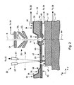
- the lens stage 23 is positioned between the objective lens 14 and the sample 16.
- the lens stage 23 includes a frame 34 which supports a first sheet portion 35 (herein also referred to as a "base region") around a first perimeter edge 36.
- the first sheet portion 35 in turn supports a second, thinner sheet portion 37 (herein also referred to as a "membrane”) around a second, inner perimeter edge 38.
- the frame 34 and the first sheet portion 35 share a layer 39 of rigid, insulating or semiconducting material, which in this example is high-resistivity (e.g. > 10 ⁇ cm) silicon (Si).
- Other rigid materials can be used, such as high-resistivity semiconductor materials, glass (i.e. SiO 2 ) or sapphire (i.e. Al 2 O 3 ).
- the frame 34, the first sheet portion 35 and the second sheet portion 37 share a layer 40 of insulating material, which in this example is silicon nitride (Si 3 N 4 ), and which preferably has low stress.
- Other insulating materials can be used, such as silicon dioxide (SiO 2 ).
- the first and second sheet portions 35, 37 are generally planar and/or have lateral dimensions (i.e. width and/or length) which are greater than its thickness.
- An aperture or passage 41 passes through first membrane portion 35 from a back face 42 (which may also be referred to as the "upstream” face or side) to a front face 43 (which may also be referred to as the "downstream” or “sample” side or face) of the lens stage 23.
- the passage 41 has a longitudinal axis which is perpendicular to the faces 42, 43.
- the tip 26 and aperture 41 are laterally spaced apart.
- the lens stage 23 is arranged such that the aperture 41 is aligned with the column's optical axis 44 along which the electron beam 8 passes. Alignment will be described in more detail later.
- At least a portion of the back face 42 of the lens stage 23 around the aperture 41 supports a first set of overlying layers providing a first electrode structure 45, herein referred to as the "back electrode structure". At least a portion of the front face 43 of the lens stage 23 around the aperture 41 supports a set of overlying patterned layers of conducting and insulating layers providing a second electrode structure or "front electrode structure" 46.
- a relatively less negative bias for example microscope ground potential
- a relatively more negative bias for example a negative potential
- a front electrode 81 for example a negative potential
- negative biases can be applied to other front electrodes 71, 72, 73 ( Figure 6 ) which can provide independent control of primary beam energy and beam focus position.
- a bias is also applied to the sample support 17, which is typically at the same bias as the electrode 81 ( Figure 6 ) in the front electrode structure 46 closest to the sample 16.
- the incident electrons 8 2 are scattered from the sample surface 47 and some of the scattered electrons 22 1 pass through the lens stage 23 and are accelerated towards the electron detector 21, which in this example is a multi-segment annular semiconductor back-scattered electron detector mounted perpendicularly to the primary electron beam 8.
- the output from the electron detector 21 is collected, stored and analysed by the control system 30.
- a current flowing to or from an electrode 81 ( Figure 6 ) in the front electrode structure 46 closest to the sample 16 (also referred to as a "sample facing electrode” or “surface electrode") can be measured and analysed by the control system 30. Current flowing through the sample 16 may be measured and analysed by the control system 30.
- surface probe microscopy can be performed using the cantilever 25 supporting a tip 26.
- a current flowing between the tip 26 and sample 16 is measured by the control system 30 and is used in a control loop to adjust tip-sample separation, d, to maintain constant current.
- Tip-sample separation, d (or s), is adjusted using the fine positioning stage 19.
- An additional or alternative fine positioning stage which supports the lens stage 23 may be used.
- a diode laser 49 directs a focused laser beam 50 onto the back face 42 of the cantilever 25 and a reflected beam 50' is measured by a photo detector 51.
- the laser 49 and photo detector 51 have an optical lever arrangement and so the photo detector 51 is in the form of a four-segment photo diode.
- an interferometer arrangement can be used. Mirrors used for guiding the laser allow the possibility of simultaneous AFM and LEEM.
- the output from the position detection system 29 is used by the control system 30 to maintain a constant cantilever deflection. In either mode, the signal provided to the fine position stage 19 also provides topographic information about the sample 16. If lateral separation between the lens stage 23 and the tip 26 is known then scanning probe data and scattering data can be correlated. Moreover, the scanning probe data can be used to set electrode potentials for the back electrode 45 and electrode(s) in the front electrode structure 46 so as to provide help to focus the electron beam 8 onto the sample surface 47.
- the lens stage 23 is mounted inside the column 2 via a mounting arm 52 which is supported by a fine positioning stage 53, such as an ANSxyz100 Scanner, which is in turn is supported on a coarse positioning stage 54, such as an ANPx100/NUM Linear Positioner.
- a fine positioning stage 53 such as an ANSxyz100 Scanner
- a coarse positioning stage 54 such as an ANPx100/NUM Linear Positioner.
- the coarse positioning stages 20, 54 are supported by a mounting block 55 which stands on the floor 56 of the sample chamber 57.
- the position sensing system 28 includes a pair of mirrors 58, 59 supported by respective adjustable mirror mounts 60, 61. Angle of tilt of the mirrors 62, 63 can be adjusted in two planes using, for example, adjustment screws 65, 66. For clarity, only one adjustment screw 65, 66 is shown for each mirror mount 60, 61.
- a 'U'-shaped electrostatic shield 67 is placed just above (i.e. upstream) and around the lens stage 23.
- the back electrode structure 45 includes an insulating layer 68 and an overlying conductive electrode 69.
- the front electrode structure 46 includes a stack 70 of layers providing electrodes 71, 72, 73 (herein referred to as "primary electrodes") separated by insulating layers 74, 75 (herein referred to as "primary inter-electrode insulating layers” or “primary inter-electrode dielectric layers”).
- primary electrodes there are three primary electrodes 71, 72, 73. However, there may be fewer or more primary electrodes.
- the stack 70 includes a second patterned layer of conductive material providing a second electrode 71 (which is also referred to herein as the "first front electrode") and an overlying co-extensive layer of insulating material 74, a third patterned layer of conductive material providing a third electrode 72 (or “second front electrode”) and an overlying co-extensive layer of insulating material 75 and a fourth patterned layer of conductive material providing a fourth electrode 73 (or "third front electrode”).
- the fourth electrode 73 partially covers the third electrode 72 which in turn partially covers the second electrode 71.
- at least a portion of each electrode 71, 72, 73 is not covered by another electrode which allows a lead to be connected.
- a pad of insulating material 76 is used to help reduce cross leakage between one electrode 71, 72, 73 and a contact lead 77 to a different electrode 71, 72, 73.
- First, second and third vias 78 ( Figure 7 ) provide access through the insulating pad 76 and through respective patterned insulating layers 71, 72, 73 to allow first, second and third contact leads 77 to contact their respective electrodes 71, 72, 73.
- the contact leads have an overlying insulating layer 79.
- An overlying layer of insulating material 80 (herein referred to as the "coating insulating layer” or “coating dielectric layer”) covers the stack 70 and contact leads 77 and contact lead insulating layer 79.
- a fifth layer of conductive material covers the layer of insulating material and provides a fifth electrode 81 (or “fourth front electrode” or “coating electrode”) and also a contact to the tip 26.
- Using five electrodes 69, 71, 72, 73, 81 can have the advantage that an electron beam cross-over can be formed within the lens stage 23 which enables a near-parallel broad beam to be projected onto the sample surface 47 for parallel imaging.
- a magnetic prism chamber (not shown), such as one described in US-B-6 878 937 , or multi-cell back-scattered electron detector can be used to enable imaging of scattered low-energy electrons in parallel imaging. Further details regarding parallel imaging is given in " Low-energy electron microscopy" by R. M. Tromp, IBM Journal of Research and Development, pp 503 to 516, volume 44 (2000 ).
- the back electrode 69 has an aperture size, d 1 , of about 8 ⁇ m
- the front electrodes 71, 72, 73, 81 have an aperture size, d 2 , of about 6 ⁇ m
- the insulating layer 40, 41, 68, 72, 74, 80 have aperture sizes, d 3 , d 4 , d 5 , d 6 , of about 12, 14, 18 and 10 ⁇ m respectively.
- the first insulating layer 39 has a thickness, t 1 , of 10 ⁇ m and the second insulating layer 40 has a thickness, t 2 , of 2 ⁇ m.
- the primary inter-electrode insulating layers 72, 74 each have a thickness, t pi1 , t pi2 , of 1.5 ⁇ m and the coating insulating layer 80 has a thickness of 0.75 ⁇ m.
- the primary electrodes 71, 72, 73 each have a thickness, t pe1 , t pe2 , t pe3 of 0.5 ⁇ m.
- the coating electrode 81 has a thickness, t ce of 0.25 ⁇ m. The thicknesses may be varied so that a layer can be thicker or thinner.
- the cantilever 25 has a width, w c , of about 50 ⁇ m and a length, l c , of about 100 ⁇ m.
- the cantilever 25 is tongue defined by a 'U' shaped slot or cut 82 which starts in the first membrane 35, passes into the second membrane 37 and ends back in the first membrane 35.
- the cantilever 25 is anchored at a proximal end 83 in the first thicker membrane portion and extends to a distal end 84 formed of thinner material.
- the tip 26 and the aperture 41 are laterally separated by a distance, u, of about 100 to 120 ⁇ m.
- the tip 26 and the aperture may be spaced by at least 5 ⁇ m, 10 ⁇ m, 20 ⁇ m, 50 ⁇ m, 100 ⁇ m or 200 ⁇ m.
- the lens 23 may be modelled to illustrate its operation and to help find lens parameters, such as values of electrode potentials.
- Electrostatic modelling is carried out using MEBS SOFEM software.
- Ray tracing is carried out using MEBS IMAGE software.
- values of spherical and chromatic aberration coefficients C S , C C can be extracted for given focus and imaging energy conditions.
- MEBS ABER-5 software can calculate the values of the coefficients C S , C C using formulae based upon the paraxial ray approximation.
- ABER-5 provides a useful comparison to results obtained from IMAGE, with the low imaging energies and large beam half angles in this arrangement, IMAGE provides more realistic C s and C c .
- MEBS WAVE software is conveniently used to calculate the beam current density profile considering the effects the diffraction, C s , C c , and extended source size.
- the potential distributions of the electrodes 69, 71, 72, 73, 81 and sample 16 is modelled using the SOFEM software package.
- the axial electrostatic potential distributions 86, 87, 88, 89, 90, 91 are calculated using the model with a unit potential applied to each electrode while the other electrodes are set at 0V. It is also assumed that the environment upstream of the back electrode 69 has the same potential of the back electrode 69. As shown in Figure 9 , the potential distributions 86, 87, 88, 89, 90, 91 overlap.
- the back electrode 69 and the first primary electrode 71 are mainly used to decelerate incoming electrodes through the application of retarding fields in a controllable manner.
- the back electrode 69 can be used to help screen any asymmetric field produced by the sample 16 and the holder 52 ( Figure 4 ) and so minimise perturbations affecting the optical properties of the system.
- the rest of the front electrodes i.e. second and third primary electrode 72, 73 and the final electrode 81, are used to adjust the final focus position of the beam 8 though this may also have some influence on the imaging energy. Some or all of these electrodes can be omitted. However, at least one of these electrodes is needed if independent control of beam energy and beam focus position is required.
- the model assumes that the sample 16 is conducting and that the final electrode 81 and the sample 16 are at the same potential. However, this need not be the case. Even so, the model is expected to provide a reasonable approximation of behaviour for a non-conducting sample.
- the membrane around the cantilever serves to screen the upper part of the column from the sample when a bias is applied to the sample. Without such screening, the electrostatic field produced by the sample may influence the space above the sample and thus alter the characteristics of the incoming beam 8.
- the lens 24 is modelled using a high accuracy ray tracing software package, namely IMAGE (version 1.3), and a ray equation and aberration integral calculation software package, namely ABER- 5 (version 1.5), which calculates the trajectory of number of primary rays based on paraxial equations.
- IMAGE version 1.3
- ABER- 5 version 1.5
- the IMAGE software package uses Hermite fits to enable high order derivatives to the off-axis fields to be calculated to high accuracy allowing the correction to paraxial approximation to be applied.
- the model shows that, for a given working distance, a low-energy electron beam (e.g. ⁇ 20 eV) can be focused on the sample surface 47 with principal on-axis aberrations and hence a current-density distribution and, therefore, spatial resolution that compares favourably with conventional low energy electron microscopes (LEEMs).
- a low-energy electron beam e.g. ⁇ 20 eV
- V 4 For a given working distance, a value of V 4 can be determined so as to focus the beam on the sample. Then C S , C C etc. can be calculated. In other words, C S and C C depend on V 4 and V 4 depends on working distance.
- Calculations are based on the dimensions given earlier, namely the electrode aperture size values d 1 , d 2 and layer thicknesses t 1 , t 2 , t pi1 , t pi2 , t ci , t pe1 , t pe2 , t pe3 , t ce specified earlier.
- the calculations determine the current-density distribution in the plane of the sample surface 47. It is assumed that the incoming primary focused electron beam 8 has a virtual cross over at a distance, z co , of 40 ⁇ m beneath the sample surface 47, a semi-angle of 5 mrad, beam energy of 500 eV with a Gaussian energy distribution of 0.5 eV 1/e full width, i.e. typical of cold field emission source.
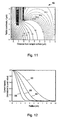
- the full line contours are lines of equipotential in steps of 1V between 21 V and 42 V relative to V 6 .
- the dashed lines are line equipotential in steps of 0.1 V between 20.1 V and 20.9 V relative to V 6 .
- the electric field is at most about 0.45 V ⁇ m -1 . Further from the optical axis, the electric field falls off rapidly.
- I is the total beam current
- ⁇ is the wavelength of the electron beam
- ⁇ 1 is the aperture angle (at the image plane)
- J ⁇ poly ⁇ IJ poly ⁇ / ⁇ 1 2
- r 1 is the distance from the central axis to the element of area d A
- r is the distance from d A to the point where J total is to be calculated.
- the image-plane brightness distribution ⁇ 0 can be characterised by its 1/ e full width, which is often called the effective demagnified source diameter, D G .
- the effective demagnified source diameter attainable depends on the design details of the column and gun. Modern SEMs provide a resolution of about 5 - 20 nm for an image energy of 500 eV (i.e. without any retarding field) and the lens 23 demagnifies the object by a factor of 3 to 4. Therefore, values of effective demagnified source diameter in the range 2 to 5 nm are considered.
- polychromatic spread functions 93, 94, 95, 96 for an on-axis beam with energies of 2, 5, 10 and 20 eV are shown.
- the polychromatic point spread function 96 for a beam energy of 20 eV shows the diameter which contains 50% of the beam current, d 50 , is 3.3 nm and that 20 - 80% current rise distance, S R 2080 , is 2.4 nm. If the beam 8 is electrically scanned through the lens unit 23, such as in the step-in mode of operation, described later, then the variation in the beam current density profile, particularly the additional blurring of the beam, with off-axis distance is considered to select an appropriate scan field size.
- Table 2 below presents the average 20 - 80% current rise distances (blur), s R Av2080 , at the optimum defocus position, z opt , for various off-axis distances , r, in the image plane, for 20 eV imaging energy.
- the optimum defocus value, z opt is the distance (directed upstream) where the minimum beam blur exists, relative to the minimum blur position for the on-axis beam.
- the best rise distance may be obtained by operating with the beam on the central axis and scanning the sample beneath the lens.
- the resolution approaches that offered by parallel LEEMs of ⁇ 5 nm at 10 eV and offers significant improvement over scanning LEEMs which offer 20 - 30 nm resolution at 20 eV. If the beam is scanned over ⁇ 150 nm from the central-axis, an improvement over scanning LEEMs is still offered.
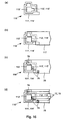
- a high-resistivity silicon wafer 97 having a thickness of about 200 ⁇ m is provided which is patterned with alignment markers (not shown) on first and second sides 98, 99 of the wafer 97 (step S1). Offsets between alignment markers (not shown) on each side of the wafer 97 can be measured by comparing them against through holes passing from one side of the wafer 97 to the other. Preferably, front side to back side alignment accuracy is better than +/- 10 ⁇ m.
- a layer 100 of silicon nitride having a thickness, t 2 , of 2 ⁇ m is deposited on the first side 98 of the wafer 97 by chemical vapour deposition (step S2).
- a first etch mask 101 is defined on the second side 99 of the wafer 97 (step S3).
- the etch mask 101 comprises a "hard” mask material, such as silicon nitride (Si 3 N 4 ) or silicon dioxide (SiO 2 ).
- the etch mask 101 may comprise a "soft" mask material, such as a photo resist or other polymeric material.
- the etch mask 101 is patterned (directly or indirectly) using optical lithographic techniques.
- a portion 102 of the wafer 97 is etched by a deep reactive ion etching process, for example using silicon hexafluoride (SiF 6 ) and oxygen (02) as a feed gas, or a similar "Bosch"-type process (step S4).
- a deep reactive ion etching process for example using silicon hexafluoride (SiF 6 ) and oxygen (02) as a feed gas, or a similar "Bosch"-type process (step S4).
- an isotropic wet etch for example comprising a mixture of hydrofluoric acid, nitric acid and acetic acid (sometime simply referred to as "HNA" can be used.
- HNA hydrofluoric acid
- etching leaves an etched wafer 97' having a pit 103 , a thinned region 104 of wafer material having a thickness, t 1 , of 10 ⁇ m and an etched back face 99'.
- a second etch mask 105 is defined on the etched back face 99' of the etched wafer 97' (step S5).
- the second etch mask 105 comprises photo resist, although another resist, such as electron-beam resist can be used.
- a region 106 of the thinned wafer 97' is etched using a wet etch, such as a mixture of potassium hydroxide (KOH), water (H 2 O) and isopropanol (step S6).
- a wet etch such as a mixture of potassium hydroxide (KOH), water (H 2 O) and isopropanol (step S6).
- first and second membranes 35, 37 are defined, following which, front and back electrodes structures are defined.
- a layer of silicon dioxide 107 having a thickness of 0.25 ⁇ m is deposited by RF magnetron sputter deposition over the etched back face 99".
- a layer 108 of tungsten (W) having a thickness of 1 ⁇ m is deposited by RF magnetron sputter deposition (step S7).
- the silicon nitride layer 100 has a front surface 109.
- an electrode stack 110 is deposited over the front surface 109 of the silicon nitride layer 100 by RF magnetron sputter deposition (steps S8, S9 & S10).
- the deposition conditions are chosen to minimize stress in this stack 110.
- the stack 110 comprises alternating layers of tungsten 111, 112, 113 and silicon dioxide 114, 115 having thicknesses of 0.5 ⁇ m and 1.5 ⁇ m respectively.
- the layers 111, 112, 113, 114, 115 are deposited in succession in a chamber (not shown) without breaking vacuum in order to improve interface quality between the dielectric and metal electrode layers.
- the electrode stack 110 is shown in more detail.
- Successive photoresist etch masks are defined and an appropriate numbers of layers etched using appropriate etches (steps S11 & S12).
- the "last" tungsten layer 113 is etched.
- the underlying silicon dioxide layer 115 is etched, followed by the "middle" tungsten layer 112.
- a potassium ferricyanide based etchant is used to etch tungsten and a hydrofluoric acid based etchant is used to etch silicon dioxide.
- etching leaves an etched stack structure 116 comprising etched tungsten layers 111', 112', 113' separated by etched silicon dioxide layers114', 115'.
- edges of the etched tungsten layers 111', 112' and corresponding paired etched silicon dioxide layers 114', 115' are shown to be co-extensive. However, the edges of the etched tungsten layers 111', 112' may recede under the corresponding silicon dioxide insulating layers114', 115'.
- a dual-layer photoresist lift off mask comprising PMGI SF6 and Shipley S1813 photo resist are applied and patterned using photolithography (step S13).
- a layer of silicon dioxide (not shown) having a thickness of 0.25 ⁇ m is deposited over the patterned mask by RF magnetron sputtering (step S14) and the resist and unwanted regions of silicon dioxide are lifted off in NMP (M-methyl-2-pyrrolidone) (step S15).
- a photoresist etch mask (not shown) is defined (step S16) and the patterned silicon dioxide layer 117 is etched using a hydrofluoric acid based (step S17).
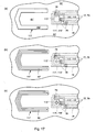
- etching leaves contact windows 78 having a size of about 3 ⁇ m ⁇ 3 ⁇ m in a patterned silicon dioxide layer117 ( Figure 16b ). Wet etching helps to provide an etched edge having a smooth rising profile over which contact leads can run. This leaves a modified partially-covered electrode structure 116".
- a dual-layer photoresist lift off mask comprising PMGI SF6 and Shipley S1813 photo resist is applied and patterned using photolithography (step S18).
- a layer of gold (not shown) having a thickness of 0.25 ⁇ m followed by a layer of silicon dioxide is deposited over the patterned mask by RF magnetron sputtering (step S19) and the resist and unwanted regions of gold are lifted off in NMP (step S20).
- a blanket layer of silicon dioxide 81' having a thickness of 0.75 ⁇ m followed by a blanket layer of tungsten 82' are deposited over the front surface 109 and the electrode structure 116"' by RF magnetron sputtering (steps S21 & 22).
- a photoresist etch mask (not shown) is applied over the tungsten layer 82' and patterned using photolithography (step S23).
- the tungsten layer 82' and silicon dioxide layer 81' are etched using a ferricyanide based wet etch and a hydrofluoric based wet etch respectively (steps S24 & S25).
- the tungsten layer 82' may be etched further using the ferricyanide based wet etch (step S26) so as to etch back the edge of the overlying tungsten electrode layer 82' so as to cause it to recede beyond the edge of the silicon dioxide layer 81'.
- etching leaves a trench 117 exposing the face 109 of the underlying silicon nitride layer 100'.
- the trench 117 is generally 'U'-shaped and outlines the subsequently-formed slot 82 ( Figure 7 ) used to form the cantilever 25 ( Figure 7 ) so as to help isolate the front and back metallization layers 81,108 ( Figure 7 ) on the cantilever 25 ( Figure 7 ). This is to reduce edge leakage and instances of surface tracking (or "flashover").
- the width of the trench is w 1 and is about 8 to 10 ⁇ m.
- Regions (not shown) of the protective silicon dioxide layers 79 close to the edge of the wafer and having an area of the order of 100 ⁇ m ⁇ 100 ⁇ m are also etched to expose regions of the gold layer for each lead 77 for providing bond bad to which wires may be bonded.
- each side 118, 119 of the processed wafer 120 are coated with a removable protective coating (not shown) such as an azide-based photoresist (step S27).
- Regions 121, 122 of the processed wafer 120 are anisotropically etched using a focused ion beam (step S28).
- the regions 121, 122 extend through the processed wafer 120 from one side 118 to the other 119.
- the width of the ion beam etch is w 2 and is about 2 ⁇ m. It is noted that the vertical and horizontal directions are not to scale.
- etching forms a cut 82' for defining the cantilever 25 ( Figure 5 ) and an aperture 41'.
- the processed wafer 120' is etched using a series of etches, namely a phosphoric acid based etch to silicon nitride, potassium hydroxide and a mixture of hydrofluoric acid, nitric acid and acetic acid etch (or "HNA") to etch silicon, a hydrofluoric acid based etch to etch silicon dioxide (step S29).
- a series of etches namely a phosphoric acid based etch to silicon nitride, potassium hydroxide and a mixture of hydrofluoric acid, nitric acid and acetic acid etch (or "HNA" to etch silicon, a hydrofluoric acid based etch to etch silicon dioxide (step S29).
- HNA acetic acid etch
- the protective layer (not shown) covering the underside 118 of the processed wafer 120' sticks to the silicon nitride layer 100 in the trench 117 ( Figure 15f ). Therefore, the protective layer (not shown) masks the bottom silicon dioxide layer 80 and electrode layer 81 from the wet etches.
- wet etching forms a wider cut 82 and a wider aperture 41.
- it sets back the edges of the dielectric layers 74, 75, 80 from the edges of the electrodes 71, 72, 73, 81. This can help to reduce charge impaction and the effects of charging.
- the protective coating is removed using acetone, rinsed in isopropanol and cleaned using an oxygen plasma (step S30)
- the probe tip 26 is deposited by electron beam induced deposition (step S31).
- step S31 Reference is made to " Automated wafer-scale fabrication of electron beam deposited tips for atomic force microscopes using pattern recognition" by J. H. Kindt et al., Nanotechnology, volume 15, page 1131 (2004 ).
- the probe tip 26 has a length lying in a range between about 5 to 10 ⁇ m and a radius lying in a range between 100 to 200 nm. The tip radius may be smaller.
- the probe tip 26 may be formed from an organic material such as amorphous carbon. However, the probe tip 26 may be formed form metals or metallic alloys.
- the lens stage 23 is then mounted in a holder 52 ( Figure 4 ) and bond wires (not shown) connected.
- the control system 30 positions the lens unit 23 ready for use (steps S33 to S38).
- the lens unit 23 is withdrawn using the positioning system 27, for example retracting the unit 23 along the x-axis (step S33). This allows the lens unit 23 to be dismounted (e.g. to be replaced) and/or to allow the sample 16 to be mounted or changed.
- the sample 16 is viewed by conventional SEM and moved into a desired position using the sample positioning system 19, 20 (step S34). Imaging can also be used to obtain other information about the sample.
- the lens unit 23 is then reinserted so that it is positioned between the objective lens 14 and the sample (step S35).
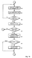
- the lens unit 23 is lowered (step S36) while separation between the lens and the sample is monitored using the lens-sample separation sensor (step S36) until the desired separation is achieved, typically when the probe tip is ⁇ 10 nm from the sample surface.
- separation may be measured in different ways.
- the output from the laser diode 51 ( Figure 2 ) or the current flowing between an electrically-biased tip 25 and the sample 16 may be monitored.
- the electrical bias may comprise low- ("dc") and high-frequency ("ac") components. Tunnelling and/or field-emission of electrons between the sample 16 and probe tip 26 can be monitored by examining the dc component. Changes in capacitance between a probe 26 and sample 16 can be monitored using the ac signal component and can use sensitive measurements of differential conductance using lock-in amplifier methods.
- the lens 23 and sample 16 are held stationary while the electron beam 8 is aligned to the centre of the aperture 41 ( Figure 2 ) of the lens unit 23 (step S38).
- This can be achieved by imaging the back face 42 ( Figure 2 ) of the lens unit 23 using SEM imaging and then placing the beam 8 in "spot" mode to align the beam 8 with the centre of the aperture 41 ( Figure 2 ).
- the lens unit 23 may be operated in a so-called “step-in” mode (steps S40 to S47) or a "stationary beam” mode (steps S49 to S65).
- the electron beam 8 is scanned, using the deflector coils 12, 13, within a given field size of the lens unit 23.
- the beam 8 can be scanned, for example, by rastering in increments of ⁇ x 1 and ⁇ y 1 (step S40).
- scattered electron data for example sample current, detector current and/or backscattered electron detector current are recorded (step S41).
- the beam 8 is scanned until the scan of the field has been completed (step S42).
- the field size can be selected from Table 2 above based on desired resolution and degree of blur. Resolution can be improved by applying dynamic compensation of the focus conditions, noting the optimum defocus positions in Table 2.
- step S43 the lens unit 23 is raised by ⁇ z 1 to a safe working distance.
- step S44 A check is made as to whether another scan in a different position is required.
- step S45 If another scan is required, then the sample 16 or lens 23 is moved from its current position to a new position offset by ⁇ x 2 , ⁇ y 2 (step S45). If the lens 23 is moved, then the beam 23 is realigned to the lens 23 (step S46).
- the lens unit 23 is lowered and another scan is performed (steps S40 to S43).
- step S48 If no further scanning is required, then operation can be stopped (step S48).
- “stationary beam” mode information about the topography of the sample 16 is obtained by scanning the probe-tip over the sample surface, while monitoring and keeping the z-separation at a desired level, and storing information about the topography the sample 16, e.g. in terms of x, y and z values (steps S49 to S52).
- a laser bounce detector can be used as the sensor, while the tip-sample separation is maintained at ⁇ 10 nm within the limits of the fine positioning stage and control response time.
- Other topography sensing modes can be used, as described earlier.
- the topography information may be processed, for example to obtain separation data (step S53).
- the tip 26 is scanned (i.e. mechanically scanned) over a given size of field (step S54).
- the lens unit 23 is raised by ⁇ z 1 to a safe distance, for example, to help avoid tip crash (step S55).
- a scan i.e. a beam scan
- a scan of the sample 16 is performed to collect low-energy electron scattering data as within the loop containing the scanning increment ⁇ x 4 , ⁇ y 4 (step S56).
- the beam 8 is continually kept aligned with the moving lens unit 23.
- a predetermined path 23 for the lens unit 23 it is possible to synchronize the beam deflection with lens unit 23 displacement.
- Topography compensation may be performed during scanning whereby the height of the sample or the electrode potentials can be adjusted so as to ensure that the low-energy electron-beam is focused as best as possible on the sample 16 (steps S59 to S62).
- the topography information collected earlier once offset by the separation between the scanning-probe tip 26 and electron beam 8) can used to determine the required adjustment in the z-position (step S61) or electrode potentials (step S62).
- step S63 scattered electron data is collected (step S63), in a similar way to that described earlier in the "step-in" mode of operation. Scanning continues until the desired scan limits have been reached (step S64). It is noted that these limits cannot exceed the travel of the piezo-actuators.
- the lens-unit is raised to a safe separation from the sample surface (step S65).
- the number of electrodes in the lens stage, the arrangement and spacing between electrodes in the lens stage and the spacing between the lens stage and the sample may differ.
- insulating materials including silicon oxynitride, and other conductive materials, such as aluminium, may be used. It will be appreciated that choice of materials may depend on processing.
- electrode potentials can be adjusted.
- electrode potentials may vary according to, among other things, primary beam energy, the number of electrodes in the lens stage, the arrangement and spacing between electrodes in the lens stage and spacing between the lens stage and the sample. These values can be found by computer modelling, as described earlier, and/or by routine experiment.
- the charged particle beam system need not be a scanning electron microscope, but can be scanning ion microscope. Those skilled in the art will appreciate that the polarity of electrode potentials are reversed and that magnitudes many need to be adjusted.
- the lens unit need not be arranged substantially parallel to the upper surface of the sample.
- the lens unit may be canted at an angle. This arrangement may be helpful when the sample is small or if the lens unit is arranged on a finger having a tip or electrode at its distal end.
- the aperture need not be disposed toward the proximate end, i.e. "backwards" of the cantilever.
- the cantilever may be "rotated" with respect to the aperture or the aperture moved such that the aperture is to one side of the distal end of the cantilever or "forwards" of the distal end of the cantilever. Either of these arrangements can be used to reduce the separation between the tip and the aperture.
- the scanning electron microscope system may be operated such that scanning probe microscopy, in particular atomic force microscopy, and scanning of the electron beam is carried out simultaneously.
- the electron microscope system may be a transmission electron microscope system.
Landscapes
- Chemical & Material Sciences (AREA)
- Analytical Chemistry (AREA)
- Physics & Mathematics (AREA)
- Health & Medical Sciences (AREA)
- General Health & Medical Sciences (AREA)
- General Physics & Mathematics (AREA)
- Nuclear Medicine, Radiotherapy & Molecular Imaging (AREA)
- Radiology & Medical Imaging (AREA)
- Analysing Materials By The Use Of Radiation (AREA)
Claims (27)
- Unité de lentille électrostatique (23) pour un système de faisceaux de particules chargées comportant :un substrat (35, 37) ayant des première et deuxième faces opposées (42, 43) et un passage (41) s'étendant entre des première et deuxième ouvertures dans les première et deuxième faces respectivement ;des première et deuxième électrodes de face (69, 81) soutenues sur les première et deuxième faces respectivement ; etun bras en porte-à-faux (25) pour sonde de surface, formé par une fente dans le substrat s'étendant entre les première et deuxième faces opposées, le bras en porte-à-faux soutenant une pointe (26) pour détecter une séparation d'échantillon lorsque l'échantillon est adjacent à la deuxième face, où le bras en porte-à-faux est latéralement espacé du passage ;où les première et deuxième électrodes de face sont agencées autour des ouvertures respectives au passage et agencées sur le bras en porte-à-faux et autour de celui-ci.
- Unité selon la revendication 1, dans laquelle le substrat (35, 37) comporte une feuille isolante (40).
- Unité selon la revendication 1 ou 2, dans laquelle le substrat (35, 37) comprend des première et deuxième parties, où la première partie (35) est plus épaisse que la deuxième partie (37).
- Unité selon la revendication 3, dans laquelle la première partie a une épaisseur d'au moins 5 µm et la deuxième partie de feuille isolante a une épaisseur de pas plus de 5µm.
- Unité selon la revendication 3 ou 4, dans laquelle la première partie du substrat soutient la deuxième partie de feuille isolante autour d'un bord périphérique.
- Unité selon l'une quelconque des revendications 3 à 5, dans laquelle les première et deuxième parties partagent une couche (40) de matériau isolant.
- Unité selon la revendication 6, dans laquelle le matériau isolant dans la couche comprend du nitrure de silicium.
- Unité selon l'une quelconque des revendications 3 à 7, dans laquelle la première partie comprend une autre couche (39) de matériau.
- Unité selon la revendication 8, dans laquelle le matériau comprend du silicium.
- Unité selon la revendication 8 ou 9, dans laquelle la deuxième partie ne comporte pas la deuxième couche de matériau.
- Unité selon l'une quelconque des revendications 3 à 10, dans laquelle le substrat est agencé de sorte à prévoir un bras en porte-à-faux (25) s'étendant de la première partie à la deuxième partie.
- Unité selon l'une des revendications précédentes, comprenant au moins deux électrodes soutenues sur la deuxième face, agencées en un empilement et autour des ouvertures du passage.
- Unité selon l'une des revendications précédentes, comprenant des troisième, quatrième et cinquième électrodes (71, 72, 73) soutenues sur la deuxième face et agencées en un empilement et autour des ouvertures du passage.
- Unité selon l'une des revendications précédentes, dans laquelle la sonde ne cache pas l'ouverture.
- Unité selon l'une des revendications précédentes, dans laquelle la sonde et l'ouverture sont espacées par au moins 10µm, préférablement au moins 20µm et plus préférablement au moins 50µm.
- Unité selon la revendication 15, dans laquelle la sonde et l'ouverture sont espacées par au moins 100µm.
- Unité selon l'une des revendications précédentes, dans laquelle le substrat est généralement plan.
- Unité selon la revendication 17, dans laquelle le substrat plan est étagé.
- Appareil comprenant :une unité de lentille selon l'une des revendications précédentes ;un moyen (18) pour soutenir un échantillon ; etun moyen (19, 20) pour positionner le support.
- Appareil selon la revendication 19, comprenant en plus :un moyen (53, 54) pour positionner l'unité de lentille électrostatique par rapport au support d'échantillon.
- Appareil selon la revendication 20 ou 21, comprenant en plus :un laser (49) agencé pour diriger la lumière sur l'unité ; etun détecteur (51) agencé pour détecter la lumière réfléchie hors de l'unité de lentille.
- Système à faisceaux de particules chargées comportant :un appareil selon la revendication 21, positionné en aval d'une lentille d'objectif.
- Procédé destiné à faire fonctionner un système à faisceaux de particules chargées qui comporte une unité de lentille électrostatique (23) comprenant un substrat (35, 37) avec des première et deuxième faces opposées (42, 43) et un passage (41) s'étendant entre des première et deuxième ouvertures dans les première et deuxième faces respectivement, des première et deuxième électrodes de face (69, 81) soutenues sur les première et deuxième faces respectivement, et un bras en porte-à-faux (25) pour sonde de surface, formé par une fente dans le substrat s'étendant entre les première et deuxième faces opposées, le bras en porte-à-faux soutenant une pointe (26) pour détecter une séparation d'échantillon où les première et deuxième électrodes sont agencées autour des ouvertures respectives du passage et agencées sur le bras en porte-à-faux et autour de celui-ci, le procédé comprenant le fait :de détecter une séparation entre l'unité de lentille et un échantillon ;de diriger un faisceau de particules chargées à travers l'unité de lentille sur l'échantillon ; etde commander l'unité de lentille électrostatique pour influencer le faisceau de particules chargées comportant la mise à la masse de la première électrode et appliquant un potentiel retardé à la deuxième électrode et à l'échantillon.
- Procédé selon la revendication 23, comprenant en plus le fait :de régler la séparation entre l'unité de lentille et un échantillon tout en détectant la séparation en utilisant la sonde.
- Procédé selon la revendication 23 ou 24, comprenant en plus le fait :de déterminer une topographie de l'échantillon en utilisant la sonde avant de balayer le faisceau de particules chargées.
- Procédé selon la revendication 25, comprenant le fait :de régler la séparation entre l'unité de lentille et l'échantillon en fonction de ladite topographie.
- Procédé selon la revendication 25 ou 26, comprenant le fait :de commander l'unité de lentille électrostatique afin de changer la focalisation en fonction de ladite topographie.
Priority Applications (2)
| Application Number | Priority Date | Filing Date | Title |
|---|---|---|---|
| EP07114130A EP2023372B1 (fr) | 2007-08-09 | 2007-08-09 | Unité de lentille électrostatique |
| DE602007009668T DE602007009668D1 (de) | 2007-08-09 | 2007-08-09 | Elektrostatische Linse |
Applications Claiming Priority (1)
| Application Number | Priority Date | Filing Date | Title |
|---|---|---|---|
| EP07114130A EP2023372B1 (fr) | 2007-08-09 | 2007-08-09 | Unité de lentille électrostatique |
Publications (2)
| Publication Number | Publication Date |
|---|---|
| EP2023372A1 EP2023372A1 (fr) | 2009-02-11 |
| EP2023372B1 true EP2023372B1 (fr) | 2010-10-06 |
Family
ID=38922732
Family Applications (1)
| Application Number | Title | Priority Date | Filing Date |
|---|---|---|---|
| EP07114130A Not-in-force EP2023372B1 (fr) | 2007-08-09 | 2007-08-09 | Unité de lentille électrostatique |
Country Status (2)
| Country | Link |
|---|---|
| EP (1) | EP2023372B1 (fr) |
| DE (1) | DE602007009668D1 (fr) |
Cited By (3)
| Publication number | Priority date | Publication date | Assignee | Title |
|---|---|---|---|---|
| WO2021114334A1 (fr) * | 2019-12-12 | 2021-06-17 | 江苏集萃微纳自动化系统与装备技术研究所有限公司 | Prc utilisé pour un système de microscope hybride afm-sem, et procédé de fabrication correspondant |
| US11040379B2 (en) | 2007-09-17 | 2021-06-22 | Bruker Nano, Inc. | Debris removal in high aspect structures |
| US11391664B2 (en) | 2007-09-17 | 2022-07-19 | Bruker Nano, Inc. | Debris removal from high aspect structures |
Families Citing this family (5)
| Publication number | Priority date | Publication date | Assignee | Title |
|---|---|---|---|---|
| FR2897719B1 (fr) * | 2006-02-20 | 2008-10-03 | Centre Nat Rech Scient | Installation et procede de nano-fabrication |
| KR101578990B1 (ko) | 2011-05-31 | 2015-12-18 | 칼 짜이스 에스엠에스 게엠베하 | 대상을 검사하는 장치 및 방법 |
| WO2015029200A1 (fr) * | 2013-08-30 | 2015-03-05 | 株式会社日立製作所 | Module de lentille pour faisceaux de particules chargées et dispositif de faisceaux de particules chargées équipé de celui-ci |
| US10107834B2 (en) | 2017-03-20 | 2018-10-23 | Infinitesima Limited | Measurement system |
| DE102018210098B4 (de) * | 2018-06-21 | 2022-02-03 | Carl Zeiss Smt Gmbh | Vorrichtung und Verfahren zum Untersuchen und/oder zum Bearbeiten einer Probe |
Family Cites Families (5)
| Publication number | Priority date | Publication date | Assignee | Title |
|---|---|---|---|---|
| US5122663A (en) * | 1991-07-24 | 1992-06-16 | International Business Machine Corporation | Compact, integrated electron beam imaging system |
| KR100339186B1 (ko) * | 1998-09-28 | 2002-05-31 | 포만 제프리 엘 | 기판상에서 패턴을 규정하는 장치 및 방법 |
| US6369385B1 (en) | 1999-05-05 | 2002-04-09 | Applied Materials, Inc. | Integrated microcolumn and scanning probe microscope arrays |
| DE102004032451B4 (de) * | 2004-07-05 | 2015-11-19 | Bernd Burchard | Vorrichtung und Verfahren zur ortsaufgelösten Platzierung von Nanoclustern |
| FR2897719B1 (fr) | 2006-02-20 | 2008-10-03 | Centre Nat Rech Scient | Installation et procede de nano-fabrication |
-
2007
- 2007-08-09 DE DE602007009668T patent/DE602007009668D1/de active Active
- 2007-08-09 EP EP07114130A patent/EP2023372B1/fr not_active Not-in-force
Cited By (5)
| Publication number | Priority date | Publication date | Assignee | Title |
|---|---|---|---|---|
| US11040379B2 (en) | 2007-09-17 | 2021-06-22 | Bruker Nano, Inc. | Debris removal in high aspect structures |
| US11391664B2 (en) | 2007-09-17 | 2022-07-19 | Bruker Nano, Inc. | Debris removal from high aspect structures |
| US11577286B2 (en) | 2007-09-17 | 2023-02-14 | Bruker Nano, Inc. | Debris removal in high aspect structures |
| US11964310B2 (en) | 2007-09-17 | 2024-04-23 | Bruker Nano, Inc. | Debris removal from high aspect structures |
| WO2021114334A1 (fr) * | 2019-12-12 | 2021-06-17 | 江苏集萃微纳自动化系统与装备技术研究所有限公司 | Prc utilisé pour un système de microscope hybride afm-sem, et procédé de fabrication correspondant |
Also Published As
| Publication number | Publication date |
|---|---|
| EP2023372A1 (fr) | 2009-02-11 |
| DE602007009668D1 (de) | 2010-11-18 |
Similar Documents
| Publication | Publication Date | Title |
|---|---|---|
| JP6905555B2 (ja) | 荷電粒子ビーム装置、荷電粒子ビーム装置のためのマルチビームブランカ、および荷電粒子ビーム装置を動作させるための方法 | |
| EP2023372A1 (fr) | Unité de lentille électrostatique | |
| US6853143B2 (en) | Electron beam system and method of manufacturing devices using the system | |
| AU2003253085B2 (en) | Charged particle beam generator | |
| JP4215282B2 (ja) | 静電対物レンズ及び電気走査装置を装備したsem | |
| JP6845900B2 (ja) | 荷電粒子ビーム装置、荷電粒子ビーム装置のためのマルチビームブランカ、および荷電粒子ビーム装置を動作させるための方法 | |
| US6771012B2 (en) | Apparatus for producing a flux of charge carriers | |
| US7067807B2 (en) | Charged particle beam column and method of its operation | |
| EP1305816B1 (fr) | Collecte d'electrons secondaires a travers l'objectif d'un microscope electronique a balayage | |
| EP1238405B1 (fr) | Procede et systeme d'examen d'un echantillon avec un faisceau de particules chargees | |
| EP1777729B1 (fr) | Microscope électronique à balayage | |
| US8481935B2 (en) | Scanning electron microscope | |
| CN113892165B (zh) | 多带电粒子束设备和方法 | |
| EP2287883A2 (fr) | Dispositif et méthode d'inspection ou de modification d'une surface à l'aide d'un faisceau de particules chargées | |
| US20240272099A1 (en) | High resolution, low energy electron microscope for providing topography information and method of mask inspection | |
| CN113906535A (zh) | 多带电粒子束设备及其操作方法 | |
| US7560691B1 (en) | High-resolution auger electron spectrometer | |
| WO2004097890A2 (fr) | Agencement de lentilles d'objectif a utiliser dans une colonne a faisceau de particules chargees | |
| US7232997B2 (en) | Apparatus and method for investigating or modifying a surface with a beam of charged particles | |
| JP2004513477A (ja) | 静電対物に調整可能な最終電極を設けたsem | |
| Zlatkin et al. | Low-energy (300 eV) versatile scanning electron microscope with 30 nm resolution |
Legal Events
| Date | Code | Title | Description |
|---|---|---|---|
| PUAI | Public reference made under article 153(3) epc to a published international application that has entered the european phase |
Free format text: ORIGINAL CODE: 0009012 |
|
| AK | Designated contracting states |
Kind code of ref document: A1 Designated state(s): AT BE BG CH CY CZ DE DK EE ES FI FR GB GR HU IE IS IT LI LT LU LV MC MT NL PL PT RO SE SI SK TR |
|
| AX | Request for extension of the european patent |
Extension state: AL BA HR MK RS |
|
| 17P | Request for examination filed |
Effective date: 20090324 |
|
| AKX | Designation fees paid |
Designated state(s): DE FR GB |
|
| GRAP | Despatch of communication of intention to grant a patent |
Free format text: ORIGINAL CODE: EPIDOSNIGR1 |
|
| GRAS | Grant fee paid |
Free format text: ORIGINAL CODE: EPIDOSNIGR3 |
|
| GRAA | (expected) grant |
Free format text: ORIGINAL CODE: 0009210 |
|
| AK | Designated contracting states |
Kind code of ref document: B1 Designated state(s): DE FR GB |
|
| REG | Reference to a national code |
Ref country code: GB Ref legal event code: FG4D |
|
| REF | Corresponds to: |
Ref document number: 602007009668 Country of ref document: DE Date of ref document: 20101118 Kind code of ref document: P |
|
| PLBE | No opposition filed within time limit |
Free format text: ORIGINAL CODE: 0009261 |
|
| STAA | Information on the status of an ep patent application or granted ep patent |
Free format text: STATUS: NO OPPOSITION FILED WITHIN TIME LIMIT |
|
| 26N | No opposition filed |
Effective date: 20110707 |
|
| REG | Reference to a national code |
Ref country code: DE Ref legal event code: R097 Ref document number: 602007009668 Country of ref document: DE Effective date: 20110707 |
|
| REG | Reference to a national code |
Ref country code: FR Ref legal event code: PLFP Year of fee payment: 10 |
|
| PGFP | Annual fee paid to national office [announced via postgrant information from national office to epo] |
Ref country code: DE Payment date: 20160802 Year of fee payment: 10 Ref country code: GB Payment date: 20160803 Year of fee payment: 10 |
|
| PGFP | Annual fee paid to national office [announced via postgrant information from national office to epo] |
Ref country code: FR Payment date: 20160712 Year of fee payment: 10 |
|
| REG | Reference to a national code |
Ref country code: DE Ref legal event code: R119 Ref document number: 602007009668 Country of ref document: DE |
|
| GBPC | Gb: european patent ceased through non-payment of renewal fee |
Effective date: 20170809 |
|
| REG | Reference to a national code |
Ref country code: FR Ref legal event code: ST Effective date: 20180430 |
|
| PG25 | Lapsed in a contracting state [announced via postgrant information from national office to epo] |
Ref country code: DE Free format text: LAPSE BECAUSE OF NON-PAYMENT OF DUE FEES Effective date: 20180301 Ref country code: GB Free format text: LAPSE BECAUSE OF NON-PAYMENT OF DUE FEES Effective date: 20170809 |
|
| PG25 | Lapsed in a contracting state [announced via postgrant information from national office to epo] |
Ref country code: FR Free format text: LAPSE BECAUSE OF NON-PAYMENT OF DUE FEES Effective date: 20170831 |