EP2023640A1 - Farbfilterarrays und Bildsensoren damit - Google Patents
Farbfilterarrays und Bildsensoren damit Download PDFInfo
- Publication number
- EP2023640A1 EP2023640A1 EP07014438A EP07014438A EP2023640A1 EP 2023640 A1 EP2023640 A1 EP 2023640A1 EP 07014438 A EP07014438 A EP 07014438A EP 07014438 A EP07014438 A EP 07014438A EP 2023640 A1 EP2023640 A1 EP 2023640A1
- Authority
- EP
- European Patent Office
- Prior art keywords
- color filters
- region
- dimensional array
- color
- color filter
- Prior art date
- Legal status (The legal status is an assumption and is not a legal conclusion. Google has not performed a legal analysis and makes no representation as to the accuracy of the status listed.)
- Withdrawn
Links
- 238000003491 array Methods 0.000 title abstract description 5
- 230000000737 periodic effect Effects 0.000 claims description 18
- 239000003086 colorant Substances 0.000 claims description 14
- 239000000758 substrate Substances 0.000 claims description 8
- 238000006243 chemical reaction Methods 0.000 claims description 6
- 239000004065 semiconductor Substances 0.000 claims description 6
- 230000005484 gravity Effects 0.000 description 24
- 239000010410 layer Substances 0.000 description 16
- 238000000926 separation method Methods 0.000 description 12
- 239000000975 dye Substances 0.000 description 9
- 230000002093 peripheral effect Effects 0.000 description 9
- 230000005693 optoelectronics Effects 0.000 description 5
- 230000001413 cellular effect Effects 0.000 description 2
- 238000010586 diagram Methods 0.000 description 2
- 238000012986 modification Methods 0.000 description 2
- 230000004048 modification Effects 0.000 description 2
- 230000003287 optical effect Effects 0.000 description 2
- 239000002344 surface layer Substances 0.000 description 2
- 206010034972 Photosensitivity reaction Diseases 0.000 description 1
- XUIMIQQOPSSXEZ-UHFFFAOYSA-N Silicon Chemical compound [Si] XUIMIQQOPSSXEZ-UHFFFAOYSA-N 0.000 description 1
- 230000002159 abnormal effect Effects 0.000 description 1
- 238000009825 accumulation Methods 0.000 description 1
- 230000000295 complement effect Effects 0.000 description 1
- 230000001788 irregular Effects 0.000 description 1
- 229910044991 metal oxide Inorganic materials 0.000 description 1
- 150000004706 metal oxides Chemical class 0.000 description 1
- 230000036211 photosensitivity Effects 0.000 description 1
- 239000000523 sample Substances 0.000 description 1
- 230000035945 sensitivity Effects 0.000 description 1
- 229910052710 silicon Inorganic materials 0.000 description 1
- 239000010703 silicon Substances 0.000 description 1
Images


Classifications
-
- H—ELECTRICITY
- H04—ELECTRIC COMMUNICATION TECHNIQUE
- H04N—PICTORIAL COMMUNICATION, e.g. TELEVISION
- H04N25/00—Circuitry of solid-state image sensors [SSIS]; Control thereof
- H04N25/10—Circuitry of solid-state image sensors [SSIS]; Control thereof for transforming different wavelengths into image signals
- H04N25/11—Arrangement of colour filter arrays [CFA]; Filter mosaics
- H04N25/13—Arrangement of colour filter arrays [CFA]; Filter mosaics characterised by the spectral characteristics of the filter elements
- H04N25/134—Arrangement of colour filter arrays [CFA]; Filter mosaics characterised by the spectral characteristics of the filter elements based on three different wavelength filter elements
Definitions
- the invention relates to image sensors, and more particularly to a color filter array for improving color symmetry in different regions of an image sensor.
- Image sensors are necessary components in many optoelectronic devices, including digital cameras, cellular phones, and toys.
- Conventional image sensors include both charge coupled device (CCD) image sensors and complementary metal oxide semiconductor (CMOS) image sensors.
- CCD charge coupled device
- CMOS complementary metal oxide semiconductor
- An image sensor typically includes a plane array of pixel cells, each pixel cell comprising a photogate, photoconductor or a photodiode having a doped region for accumulating photo-generated charge.
- a periodic pattern of dyes of different colors is superimposed over the plane array of pixel cells. This pattern is known as a color filter array (CFA).
- CFA color filter array
- a plurality of microlenses is superimposed over the color filter array (CFA).
- a square, or circular microlens is utilized to focus light onto one initial charge accumulation region of each of pixel cells. By collecting light from a large light collecting area and focusing it on a small photosensitive area of the image sensor microlenses may significantly improve the image sensor photosensitivity.
- Figs. 1 and 2 are schematic diagrams showing an image sensor 10 disclosed in U. S. patent No. 6,995,800 issued to Takahashi et al.
- Fig. 1 shows a plan view of a pixel group
- Fig. 2 shows a cross sectional view of the pixels in the first, third and fifth columns of the pixel group shown in Fig. 1 .
- reference numeral 1 represents a pixel having a photodiode or photoelectric conversion element 5 formed in the surface layer of a silicon substrate (Si substrate) 18.
- Reference numeral 2 represents a light-shielding layer having a light-shielding area for shielding the area of the pixel 1 excepting the photodiode 5.
- Reference numeral 3 represents an opening area formed through the light-shielding layer 2 through which light is incident upon the photodiode 5.
- Reference numeral 4 represents a microlens for converging light on the photodiode 5.
- Reference numeral 6 represents a color filter layer of red, green, blue or other colors. Although only a 5x5 pixels is shown in Fig. 1 for the purposes of simplicity, there may in practice be several hundred thousands to several millions of pixels disposed two-dimensionally.
- Figs. 1 and 2 show the pixel 1 disposed nearer the peripheral area than the center of the pixel group has a center of gravity of the light reception area of the photodiode 5 positioned nearer to the peripheral area than the centers of gravity of the microlens 4 and opening area 3.
- the optical axis of light converged by the microlens 4 thus becomes coincident with the center of gravity of the light reception area of the photodiode 5.
- the pixel 1 of the first column has the centers of gravity of the microlens 4 and opening area 3 positioned to the right as viewed in Fig. 1 relative to the center of gravity of the light reception area of the photodiode 5.
- the pixel 1 of the third column has the centers of gravity of the microlens 4 and opening area 3 positioned at the center of gravity of the light reception area of the photodiode 5.
- the pixel 1 of the fifth column has the centers of gravity of the microlens 4 and opening area 3 positioned to the left as viewed in Fig. 2 relative to the center of gravity of the light reception area of the photodiode 5.
- the pixel 1 disposed nearer to the peripheral area than the center of the pixel group has a center of gravity of the photodiode 5 positioned nearer to the peripheral area than the centers of gravity of the microlens 4 and opening area 3.
- light passing through the microlens 4 and being incident upon the photodiode 5 is not intercepted by the light-shielding area of the light-shielding layer 2.
- a difference between the maximum and minimum values of output signals of the pixels at different locations in the image sensor illustrated in Figs. 1 and 2 can thus be reduced to a level less than 10% of the average of the output signals. This is because light converged on the photodiode 5 is not intercepted by the light-shielding layer 2 and a variation in light reception sensitivities can be reduced.
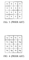
- the color filter layer 6 used in the image sensor 10 illustrated in Figs. 1 and 2 can be a two-dimensional color filter array (CFA) including a periodic pattern of dyes of different primary colors such as red (R), green (G) and blue (B) filters, as illustrated in Fig. 3 .
- the periodic pattern illustrated in Fig. 3 is a so-called Bayer pattern, including a red (R) filter, a blue (B) filter and a pair of green (G) filters.
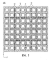
- the color filter layer 6 illustrated in Figs. 1 and 2 can also be a two-dimensional color filter array including a periodic pattern of a cyan (Cy) filter, a magenta (Mg) filter and a pair of yellow (Ye) filters, as illustrated in Fig. 4 .
- Fig. 1 Although the output signal variation of pixels at different locations in an image sensor can be improved by the relative arrangement illustrated in Fig. 1 .
- Some issues such as "color separation" may occur in an image sensor with structures similar to that illustrated in Figs. 1 and 2 . Color separation may be discovered when an image sensor is subjected to a chip probe (CP) test in which an image sensor is examined under a collimated white light. Color separation may occur in the photodiode or photoelectric conversion element 5 when the image sensor is formed in an irregular pattern rather a radially symmetrical pattern due to line routing or other device design requirements. An image sensor suffering from color separation may cause "image shading" in an optoelectronic device using the image sensor, thus, optoelectronic device may display abnormal images.
- CP chip probe
- Attachments 1 and 2 are simulated images of an image sensor (not shown) having a structure similar to that illustrated in Fig. 1 , wherein the image sensor incorporates a CFA arranged in the Bayer pattern illustrated in Fig. 3 .
- the simulated images were obtained by a CP test using a collimated white light, wherein attachment 1 shows a simulated image obtained by the image sensor having photodiodes with only one-axial asymmetrical, such as with x-axial asymmetrical, and attachment 2 shows a simulated image obtained by an image sensor having photodiodes with at least two-axial asymmetries, such as x-axial and y-axial asymmetries.
- the simulated image shows an uneven image profile presenting a red-deflected color at an upper portion of the image sensor and a blue-deflected color at a lower portion of the image sensor.
- the illustrated image shows an uneven image profile presenting a red-deflected color at an upper-left portion of the image sensor, a blue-deflected color at a lower- right portion of the image sensor, and a green-deflected color at an upper-right portion and a lower-left portion of the image sensor.
- the invention provides color filter arrays (CFA) and image sensors using the same for reducing or preventing color separation.
- CFA color filter arrays
- An exemplary embodiment of a color filter array comprises a two-dimensional array including a plurality of first color filters, a plurality of second color filters, and a plurality of third color filters, wherein the first, second and third color filters are periodically arranged, and at least the first, second and third color filters formed in a first region of the two-dimensional array and the first, second and third color filters formed in a second region of the two-dimensional array are symmetrically mirrored.
- An exemplary embodiment of an image sensor comprises a semiconductor substrate with a plurality of photoelectric conversion elements formed therein.
- a light-shielding layer comprising a plurality of opening areas, each exposing a part of the photodiode, is formed over the semiconductor substrate.
- a color filter array is superimposed over the light-shielding layer, wherein the color filer array comprises a two-dimensional array comprising a plurality of first color filters, a plurality of second color filters, and a plurality of third color filters.
- a plurality of microlens superimposes over the color filter array, each covering the opening area of the underlying light-shielding layer.
- the first, second and third color filters are periodically arranged, and at least the first, second and third color filters formed in a first region of the two-dimensional array and the first, second and third color filters formed in a second region of the two-dimensional array are symmetrically mirrored.
- Fig. 1 is a schematic top view showing a conventional image sensor
- Fig. 2 is a cross sectional view of pixels in the first, third and fifth columns of the image sensor shown in Fig. 1 ;
- Fig. 3 shows a conventional color filter array including a pattern of red (R), green (G) and blue (B) filters;
- Fig. 4 shows a conventional color filter array including a pattern of cyan (Cy), magenta (Mg), yellow (Ye) filters;
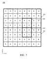
- Fig. 5 is a schematic top view showing an image sensor according to an embodiment of the invention.
- Fig. 6 is a cross sectional view of pixels in the first, fourth and eighth columns of the image sensor shown in Fig. 5 ;
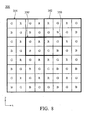
- Fig. 7 shows a color filter array including a pattern of red (R), green (G) and blue (B) filters according to an embodiment of the invention
- Fig. 8 shows an arrangement of a color filter array including a pattern of red (R), green (G) and blue (B) filters according to another embodiment of the invention.
- Fig. 9 shows an arrangement of a color filter array including a pattern of red (R), green (G) and blue (B) filters according to yet another embodiment of the invention.
- Figs. 5 and 6 are schematic diagrams showing an image sensor 100 according to an exemplary embodiment of the invention.
- Fig. 5 shows a plan view of a pixel group of the image sensor 100 and Fig. 6 shows a cross sectional view of pixels in the first, third/fourth and eighth columns of the pixel group shown in Fig. 5 .
- reference numeral 30 represents a pixel having a photodiode or photoelectric conversion element 35 formed in the surface layer of a semiconductor substrate (e.g. a Si substrate) 38.
- Reference numeral 32 represents a light-shielding layer having a light-shielding area for shielding the area of the pixel 30 excepting the photodiode 35.
- Reference numeral 33 represents an opening area formed through the light-shielding layer 32 through which light is incident upon the photodiode 35.
- Reference numeral 34 represents a microlens for converging light on the photodiode 35.
- Reference numeral 36 represents a color filter layer of red, green, blue, or other colors.
- the pixel 30 disposed nearer the peripheral area than the center of the pixel group has a center of gravity of the light reception area of the photodiode 35 positioned nearer the peripheral area than the centers of gravity of the microlens 34 and opening area 33.
- the optical axis of light converged by the microlens 34 thus becomes coincident with the center of gravity of the light reception area of the photodiode 35.
- the pixel 30 of the first column has the centers of gravity of the microlens 34 and opening area 33 positioned to the right as shown in Fig. 5 relative to the center of gravity of the light reception area of the photodiode 35.
- the pixel 30 of the fourth and fifth columns have the centers of gravity of the microlens 34 and opening area 33 positioned at the center of gravity of the light reception area of the photodiode 35.
- the pixel 30 of the eighth column has the centers of gravity of the microlens 34 and opening area 33 positioned to the left as viewed in Fig. 6 relative to the center of gravity of the light reception area of the photodiode 35.
- the center of gravity of the opening area 33 is the center of gravity of an optional mass disposed in the opening area 33.
- the pixel 30 disposed nearer to the peripheral areanearer the peripheral area than the center of the pixel group center of gravity of the photodiode 35 positioned nearer to the peripheral area than the centers of gravity of the microlens 34 and opening area 33.
- the light-shielding area of the light-shielding layer 32 does not intercept light passing through the microlens 34 to be incident on the photodiode 35.
- a difference between the maximum and minimum values of output signals of the pixels in the image sensor 100 at different locations in the image sensor of Figs. 5 and 6 can be reduced to a level less than 10% of the average of output signals but formed with color separation issues.
- the patterns of the color filter layer 36 of the image sensor 100 illustrated in Figs. 5 and 6 are modified as described in the following to further reduce or prevent color separation.
- Fig. 7 shows a color filter array including a periodic pattern of red (R), green (G) and blue (B) filters according to an embodiment of the invention.
- an exemplary color filter array 300 for the color filter layer 36 is provided for the purpose of reducing even preventing color separation issues of an image sensor, especially while the photodiodes 35 used in the image sensor 100 are x-axial asymmetrical patterns (not shown).
- the color filter array 300 is illustrated as a two-dimensional color filter array substantially divided into two regions 302 and 304 along a center of the color filter array 300 in an x-direction, each including a periodic pattern of dyes of different primary colors such as red (R), green (G) and blue (B) filters.
- the region 302 of the color filter array 300 is illustrated as an upper region of the color filter array 300 and the region 304 color filter array 300 is illustrated as a lower region of the color filter array 300 in Fig. 7 .
- the periodic pattern of red (R), green (G) and blue (B) filters of the color filter array 300 are arranged in a Bayer pattern 350 which includes one R filter, one B filter, and a pair of G filters.
- the patterns of the color filter array 300 in the region 304 are arranged as a periodic pattern of dyes of different colors such as red (R), green (G) and blue (B) filters but with a modified Bayer pattern configuration different from the Bayer pattern configuration 350 in the region 302.
- the modified Bayer pattern configuration 350' in the region 304 and the Bayer pattern configuration 350 in the region 302 are mirror symmetrical. Accordingly, the periodic pattern of dyes the R, G and B filters in the region 302 and 304 are symmetrically mirrored against an x-direction.
- Attachment 3 shows a simulated image of an image sensor incorporating the CFA 300 illustrated in Fig. 7 having photodiodes in asymmetrical x-axial patterns.
- the simulated image is obtained in a CP test using a collimated white light.
- the simulated image shows an even image profile presenting no red-deflected color in an upper portion (i.e. the region 302) of the image sensor and no blue-deflected color in a lower portion (i.e. the region 304) of the image sensor.
- a symmetrical image profile with even color uniformity and color symmetry is obtained and the conventional color separation issue is thus reduced or even prevented.
- An image with better white balance can be also provided.
- Fig. 8 shows an arrangement of a color filter array including a pattern of red (R), green (G) and blue (B) filters according to another embodiment of the invention.
- the color filter array 300 illustrated in Fig. 7 is modified while the photodiodes 35 used in the image sensors are of asymmetrical y-axial patterns (not shown), as shown in Fig. 8 .
- the color filter array 300 is substantially divided into two regions 302 and 304 at a center of the color filter array 300 along a y-direction.
- the region 302 of the color filter array 300 is illustrated as a right region of the color filter array 300 and the region 304 of the color filter array 300 is illustrated as a left region of the color filter array 300.
- the periodic pattern of red (R), green (G) and blue (B) filters of the color filter array 300 are arranged in a Bayer pattern configuration 350 which including one R filter, one B filter, and a pair of G filters.
- the patterns of the color filter array 300 in the region 304 are arranged as a periodic pattern of dyes of different colors such as red (R), green (G) and blue (B) filters but with a modified Bayer pattern configuration different from the Bayer pattern configuration 350 in the region 302.
- the modified Bayer pattern configuration 350' in the region 304 and the Bayer pattern configuration 350 in the region 302 are symmetrically mirrored. Accordingly, the periodic pattern of dyes the R, G and B filters in the region 302 and 304 are symmetrically mirrored against an x-direction. Accordingly, a symmetrical image profile can be obtained but, for simplicity, are not shown here, and the conventional color separation is thus reduced or even prevented. An image with better white balance can be also provided.
- Fig. 9 shows an arrangement of a color filter array including a pattern of red (R), green (G) and blue (B) filters according to yet another embodiment of the invention.
- a color filter array 400 is a two-dimensional color filter array substantially divided into four regions 402, 404, 406 and 408 clockwise along a center of the color filter array 300 along both x and y directions, each including a periodic pattern of dyes of different colors such as red (R), green (G) and blue (B) filters.
- the region 402 of the color filter array 400 is illustrated as an upper-right region of the color filter array 400
- the region 404 of the color filter array 400 is illustrated as a lower-right region of the color filter array 300
- the region 406 of the color filter array 400 is illustrated as an lower-left region of the color filter array 400
- the region 404 of the color filter array 400 is illustrated as an upper-left region of the color filter array 400.
- the periodic pattern of red (R), green (G) and blue (B) filters of the color filter array 400 is arranged as Bayer pattern 450 which includes one R filter, one B filter, and a pair of G filters.
- the patterns of the color filter array 400 in the regions 404, 406 and 408 are arranged as a periodic pattern of dyes of different colors such as red (R), green (G) and blue (B) filters but with a modified Bayer pattern configuration different from the Bayer pattern configuration 450 in the region 402.
- the modified Bayer pattern configuration 450' in the regions 404 and the Bayer pattern configuration 450 in the region 402 are symmetrically mirrored corresponding to the x-axis.
- the modified Bayer pattern configuration 450'" in the regions 408 and the Bayer pattern configuration 450 in the region 402 are symmetrically mirrored corresponding to the y-axis.
- the modified Bayer pattern configuration 450" in the regions 406 is symmetrically mirrored corresponding to the y-axis with the modified Bayer pattern configurations 450' in the region 404 and is symmetrically mirrored corresponding to the x-axis with the modified Bayer pattern configurations 450'" in the region 408.
- the modified Bayer pattern configuration 450" in region 406 is also symmetrically radial corresponding to the Bayer pattern configuration 450 in the region 402.
- Attachment 4 shows a simulated image of an image sensor incorporating the CFA 400 illustrated in Fig. 9 and having photodiodes of both x-axial and y-axial asymmetrical patterns.
- the simulated image is obtained in a CP test using a collimated white light.
- the illustrated image shows an even image profile presenting no red -deviated color at an upper-left portion (i.e. the region 408) of the image sensor, no blue-deviated color at a lower-right portion (i.e. the region 404) of the image sensor, and no green-deviated color at an upper-right and a lower-left and portions (i.e. the region 402 and 406, respectively) of the image sensor.
- a symmetrical image profile is obtained and the conventional color separation is thus reduced or even prevented.
- An image with better white balance can be also provided.
- the color filter arrays 300 and 400 illustrated in Figs. 7 , 8 and 9 are illustrated as two-dimensional color filter array including a periodic pattern of red (R), green (G) and blue (B) filters and are not limited thereto.
- the color filter arrays 300 and 400 illustrated in Figs. 7 , 8 and 9 can additionally be a two-dimensional color filter array including a periodic pattern of different colors of cyan (Cy), magenta (Mg), yellow (Ye) filters.
- the red pattern can be substituted by the cyan pattern
- the green pattern can be substituted by the yellow pattern
- the blue pattern can be substituted by the magenta pattern.
- the signal output of the photodiode or photoelectric conversion elements in the region covered by such modified CFA patterns illustrated in, for example, Fig. 7 , 8 or 9 is to be suitably adjusted by wire routing or by software to conform to image protocols for correctly presenting an image.
Landscapes
- Physics & Mathematics (AREA)
- Spectroscopy & Molecular Physics (AREA)
- Engineering & Computer Science (AREA)
- Multimedia (AREA)
- Signal Processing (AREA)
- Solid State Image Pick-Up Elements (AREA)
- Color Television Image Signal Generators (AREA)
Priority Applications (1)
| Application Number | Priority Date | Filing Date | Title |
|---|---|---|---|
| EP07014438A EP2023640A1 (de) | 2007-07-23 | 2007-07-23 | Farbfilterarrays und Bildsensoren damit |
Applications Claiming Priority (1)
| Application Number | Priority Date | Filing Date | Title |
|---|---|---|---|
| EP07014438A EP2023640A1 (de) | 2007-07-23 | 2007-07-23 | Farbfilterarrays und Bildsensoren damit |
Publications (1)
| Publication Number | Publication Date |
|---|---|
| EP2023640A1 true EP2023640A1 (de) | 2009-02-11 |
Family
ID=38738111
Family Applications (1)
| Application Number | Title | Priority Date | Filing Date |
|---|---|---|---|
| EP07014438A Withdrawn EP2023640A1 (de) | 2007-07-23 | 2007-07-23 | Farbfilterarrays und Bildsensoren damit |
Country Status (1)
| Country | Link |
|---|---|
| EP (1) | EP2023640A1 (de) |
Citations (3)
| Publication number | Priority date | Publication date | Assignee | Title |
|---|---|---|---|---|
| US5757520A (en) | 1994-12-13 | 1998-05-26 | Fuji Xerox Co., Ltd. | Color linear image sensor and an image processing system |
| EP0967795A2 (de) | 1998-06-22 | 1999-12-29 | Eastman Kodak Company | Parallele Ausgangsarchitekturen für aktive CMOS-Bildsensoren |
| US20020135689A1 (en) | 2001-03-08 | 2002-09-26 | Fuji Photo Film Co., Ltd. | Solid-state image pickup device and control thereof |
-
2007
- 2007-07-23 EP EP07014438A patent/EP2023640A1/de not_active Withdrawn
Patent Citations (3)
| Publication number | Priority date | Publication date | Assignee | Title |
|---|---|---|---|---|
| US5757520A (en) | 1994-12-13 | 1998-05-26 | Fuji Xerox Co., Ltd. | Color linear image sensor and an image processing system |
| EP0967795A2 (de) | 1998-06-22 | 1999-12-29 | Eastman Kodak Company | Parallele Ausgangsarchitekturen für aktive CMOS-Bildsensoren |
| US20020135689A1 (en) | 2001-03-08 | 2002-09-26 | Fuji Photo Film Co., Ltd. | Solid-state image pickup device and control thereof |
Similar Documents
| Publication | Publication Date | Title |
|---|---|---|
| US20090027527A1 (en) | Color filter arrays and image sensors using the same | |
| US8164042B2 (en) | Color filter arrays and image sensors using the same | |
| US10015416B2 (en) | Imaging systems with high dynamic range and phase detection pixels | |
| US10032810B2 (en) | Image sensor with dual layer photodiode structure | |
| US20250393324A1 (en) | CMOS Image Sensors with Per-Pixel Micro-Lens Arrays | |
| CN208093559U (zh) | 图像像素 | |
| CN106549026B (zh) | 固态成像装置 | |
| US7902618B2 (en) | Backside illuminated imaging sensor with improved angular response | |
| US7507944B1 (en) | Non-planar packaging of image sensor | |
| JP6141024B2 (ja) | 撮像装置および撮像システム | |
| US12289545B2 (en) | Image sensing device including light shielding pattern | |
| EP2680591B1 (de) | Farbbildformungsvorrichtung | |
| US20060169870A1 (en) | Image sensor with embedded optical element | |
| US7019279B2 (en) | Solid-state image sensor with the optical center of microlenses shifted from the center of photo-sensors for increasing the convergence ratio | |
| KR20240091440A (ko) | 서로 다른 크기의 마이크로 렌즈를 포함하는 이미지 센서 | |
| KR100837454B1 (ko) | 고체 촬상 장치 | |
| JP2004172278A (ja) | カラー固体撮像装置 | |
| US20070273777A1 (en) | Solid-state imaging device | |
| JP2004186311A (ja) | Mos型イメージセンサ及びデジタルカメラ | |
| EP2023640A1 (de) | Farbfilterarrays und Bildsensoren damit | |
| US6744032B1 (en) | Arrangement of microlenses in a solid-state image sensor for improving signal to noise ratio | |
| JP2003234965A (ja) | 撮像素子 | |
| JP2011061081A (ja) | イメージセンサ | |
| JP4419658B2 (ja) | 固体撮像装置 | |
| TW200905870A (en) | Color filter arrays and image sensors using the same |
Legal Events
| Date | Code | Title | Description |
|---|---|---|---|
| PUAI | Public reference made under article 153(3) epc to a published international application that has entered the european phase |
Free format text: ORIGINAL CODE: 0009012 |
|
| 17P | Request for examination filed |
Effective date: 20080930 |
|
| AK | Designated contracting states |
Kind code of ref document: A1 Designated state(s): AT BE BG CH CY CZ DE DK EE ES FI FR GB GR HU IE IS IT LI LT LU LV MC MT NL PL PT RO SE SI SK TR |
|
| AX | Request for extension of the european patent |
Extension state: AL BA HR MK RS |
|
| AKX | Designation fees paid |
Designated state(s): AT BE BG CH CY CZ DE DK EE ES FI FR GB GR HU IE IS IT LI LT LU LV MC MT NL PL PT RO SE SI SK TR |
|
| STAA | Information on the status of an ep patent application or granted ep patent |
Free format text: STATUS: THE APPLICATION IS DEEMED TO BE WITHDRAWN |
|
| 18D | Application deemed to be withdrawn |
Effective date: 20101002 |