EP2027649B1 - Système et procédé pour constituer un circuit émetteur pour une modulation polaire et une linéarisation d'amplificateur de puissance - Google Patents
Système et procédé pour constituer un circuit émetteur pour une modulation polaire et une linéarisation d'amplificateur de puissance Download PDFInfo
- Publication number
- EP2027649B1 EP2027649B1 EP07812024A EP07812024A EP2027649B1 EP 2027649 B1 EP2027649 B1 EP 2027649B1 EP 07812024 A EP07812024 A EP 07812024A EP 07812024 A EP07812024 A EP 07812024A EP 2027649 B1 EP2027649 B1 EP 2027649B1
- Authority
- EP
- European Patent Office
- Prior art keywords
- amplifier
- output
- amplitude
- transmitter
- signal
- Prior art date
- Legal status (The legal status is an assumption and is not a legal conclusion. Google has not performed a legal analysis and makes no representation as to the accuracy of the status listed.)
- Not-in-force
Links
- 238000000034 method Methods 0.000 title claims description 11
- 238000001514 detection method Methods 0.000 claims abstract description 16
- 238000004891 communication Methods 0.000 claims abstract description 7
- 238000012937 correction Methods 0.000 description 6
- 230000008901 benefit Effects 0.000 description 2
- 230000007423 decrease Effects 0.000 description 2
- 230000008569 process Effects 0.000 description 2
- 230000005540 biological transmission Effects 0.000 description 1
- 239000000470 constituent Substances 0.000 description 1
- 230000000694 effects Effects 0.000 description 1
- 230000008030 elimination Effects 0.000 description 1
- 238000003379 elimination reaction Methods 0.000 description 1
- 238000001914 filtration Methods 0.000 description 1
- 238000002347 injection Methods 0.000 description 1
- 239000007924 injection Substances 0.000 description 1
- 238000004519 manufacturing process Methods 0.000 description 1
- 238000005259 measurement Methods 0.000 description 1
- 238000012986 modification Methods 0.000 description 1
- 230000004048 modification Effects 0.000 description 1
- 230000004044 response Effects 0.000 description 1
- 238000012546 transfer Methods 0.000 description 1
Images


Classifications
-
- H—ELECTRICITY
- H04—ELECTRIC COMMUNICATION TECHNIQUE
- H04B—TRANSMISSION
- H04B1/00—Details of transmission systems, not covered by a single one of groups H04B3/00 - H04B13/00; Details of transmission systems not characterised by the medium used for transmission
- H04B1/02—Transmitters
- H04B1/04—Circuits
- H04B1/0483—Transmitters with multiple parallel paths
-
- H—ELECTRICITY
- H03—ELECTRONIC CIRCUITRY
- H03C—MODULATION
- H03C5/00—Amplitude modulation and angle modulation produced simultaneously or at will by the same modulating signal
-
- H—ELECTRICITY
- H03—ELECTRONIC CIRCUITRY
- H03F—AMPLIFIERS
- H03F1/00—Details of amplifiers with only discharge tubes, only semiconductor devices or only unspecified devices as amplifying elements
- H03F1/02—Modifications of amplifiers to raise the efficiency, e.g. gliding Class A stages, use of an auxiliary oscillation
- H03F1/0205—Modifications of amplifiers to raise the efficiency, e.g. gliding Class A stages, use of an auxiliary oscillation in transistor amplifiers
-
- H—ELECTRICITY
- H03—ELECTRONIC CIRCUITRY
- H03F—AMPLIFIERS
- H03F1/00—Details of amplifiers with only discharge tubes, only semiconductor devices or only unspecified devices as amplifying elements
- H03F1/32—Modifications of amplifiers to reduce non-linear distortion
- H03F1/3241—Modifications of amplifiers to reduce non-linear distortion using predistortion circuits
- H03F1/3282—Acting on the phase and the amplitude of the input signal
-
- H—ELECTRICITY
- H03—ELECTRONIC CIRCUITRY
- H03F—AMPLIFIERS
- H03F1/00—Details of amplifiers with only discharge tubes, only semiconductor devices or only unspecified devices as amplifying elements
- H03F1/32—Modifications of amplifiers to reduce non-linear distortion
- H03F1/3241—Modifications of amplifiers to reduce non-linear distortion using predistortion circuits
- H03F1/3282—Acting on the phase and the amplitude of the input signal
- H03F1/3288—Acting on the phase and the amplitude of the input signal to compensate phase shift as a function of the amplitude
-
- H—ELECTRICITY
- H03—ELECTRONIC CIRCUITRY
- H03F—AMPLIFIERS
- H03F1/00—Details of amplifiers with only discharge tubes, only semiconductor devices or only unspecified devices as amplifying elements
- H03F1/34—Negative-feedback-circuit arrangements with or without positive feedback
-
- H—ELECTRICITY
- H03—ELECTRONIC CIRCUITRY
- H03F—AMPLIFIERS
- H03F3/00—Amplifiers with only discharge tubes or only semiconductor devices as amplifying elements
- H03F3/20—Power amplifiers, e.g. Class B amplifiers, Class C amplifiers
- H03F3/24—Power amplifiers, e.g. Class B amplifiers, Class C amplifiers of transmitter output stages
-
- H—ELECTRICITY
- H03—ELECTRONIC CIRCUITRY
- H03G—CONTROL OF AMPLIFICATION
- H03G3/00—Gain control in amplifiers or frequency changers
- H03G3/20—Automatic control
- H03G3/30—Automatic control in amplifiers having semiconductor devices
- H03G3/3036—Automatic control in amplifiers having semiconductor devices in high-frequency amplifiers or in frequency-changers
- H03G3/3042—Automatic control in amplifiers having semiconductor devices in high-frequency amplifiers or in frequency-changers in modulators, frequency-changers, transmitters or power amplifiers
- H03G3/3047—Automatic control in amplifiers having semiconductor devices in high-frequency amplifiers or in frequency-changers in modulators, frequency-changers, transmitters or power amplifiers for intermittent signals, e.g. burst signals
-
- H—ELECTRICITY
- H04—ELECTRIC COMMUNICATION TECHNIQUE
- H04W—WIRELESS COMMUNICATION NETWORKS
- H04W52/00—Power management, e.g. Transmission Power Control [TPC] or power classes
- H04W52/04—Transmission power control [TPC]
- H04W52/30—Transmission power control [TPC] using constraints in the total amount of available transmission power
- H04W52/36—Transmission power control [TPC] using constraints in the total amount of available transmission power with a discrete range or set of values, e.g. step size, ramping or offsets
- H04W52/367—Power values between minimum and maximum limits, e.g. dynamic range
-
- H—ELECTRICITY
- H04—ELECTRIC COMMUNICATION TECHNIQUE
- H04W—WIRELESS COMMUNICATION NETWORKS
- H04W52/00—Power management, e.g. Transmission Power Control [TPC] or power classes
- H04W52/04—Transmission power control [TPC]
- H04W52/52—Transmission power control [TPC] using AGC [Automatic Gain Control] circuits or amplifiers
-
- H—ELECTRICITY
- H03—ELECTRONIC CIRCUITRY
- H03F—AMPLIFIERS
- H03F2200/00—Indexing scheme relating to amplifiers
- H03F2200/207—A hybrid coupler being used as power measuring circuit at the output of an amplifier circuit
-
- H—ELECTRICITY
- H04—ELECTRIC COMMUNICATION TECHNIQUE
- H04B—TRANSMISSION
- H04B1/00—Details of transmission systems, not covered by a single one of groups H04B3/00 - H04B13/00; Details of transmission systems not characterised by the medium used for transmission
- H04B1/02—Transmitters
- H04B1/04—Circuits
- H04B2001/0408—Circuits with power amplifiers
- H04B2001/0433—Circuits with power amplifiers with linearisation using feedback
Definitions
- the invention generally relates to systems and methods for transmitting and receiving wireless communication, and relies in particular to transceivers for wireless telecommunication systems.
- Modulation of a carrier with a baseband signal can be achieved using a polar representation of the signal representing the baseband signal as magnitude and phase components. These components are translated onto an RF carrier by functional blocks that modulate the carrier phase and amplitude independently. For reasons of power efficiency combining the component signals is ideally performed at the final stage of the transmitter, which typically is a non-linear power amplifier (PA). When a modulator is implemented in this fashion, time-alignment of the phase and magnitude components is critical for modulated signal integrity.
- PA non-linear power amplifier
- Polar closed-loop systems have been used for many years in transmitter systems.
- Polar-Loop Transmitter by V. Petrovic & W. Gosling, Electronics Letters, vol.15 No. 10, (1979 ) discloses a polar-loop transmitter.
- U.S. Patent No. 6,801,784 discloses a continuous closed-loop control system for a wireless transceiver power amplifier that includes modulation injection. See also, An IC for Linearizing RF Power Amplifiers Using Envelope Elimination and Restoration by Su and McFarland, IEEE, JSSC, Dec. 1988 , which also discloses systems for closed-loop envelope control.
- phase modulation of a earner is achieved through the use of a phase locked loop.
- Most common PLL implementations includes a phase-locked loop implementation as an offset PLL with a Type 2 loop transfer function (i.e., two poles at zero frequency). Output amplitude (and therefore power) control is typically obtained by using a Type 1 loop.
- WO 02/47249 and WO 02/060088 disclose known polar loop amplifier arrangements.
- Polar modulators typically have strict time-alignment requirements between the phase and amplitude components. Control of timing-alignment requires control of open-loop gain and bandwidth (3dB) and phase response of the loops. Maintaining timing alignment over a range of power levels is difficult in certain applications due to non-idealities in the components used.
- a transmitter circuit for use in a multi-frequency wireless communication system, said transmitter circuit comprising an input modulation unit for receiving at least one signal that is representative of information to be modulated; a phase modulation system coupled to the output of the input modulation unit for providing a phase modulation on an output signal (V OUT ), said phase modulation system including a phase detection system and an adjustable power amplifier; and an amplitude modulation system for providing amplitude modulation on the output signal, characterised in that the amplitude modulation system is coupled to receive the output of the input modulation unit and the output of the adjustable power amplifier, and includes an amplitude detection system comprising a variable gain amplifier 58 coupled to receive an error signal (V err ) derived from the output of the input modulation unit and the output of the adjustable power amplifier, wherein the gain of the variable gain amplifier is controlled using a ramp voltage (V RAMP ) related to the output power, and wherein the variable gain amplifier provides a control signal V( APC ) for controlling the
- a method for generating an output signal in a transmitter circuit for use in a multi-frequency wireless communication system comprising the steps of receiving at a modulation unit at least one signal that is representative of information to be modulated; providing a phase modulation on the output signal using a phase locked loop and an adjustable power amplifier; and providing amplitude modulation on the output signal using an amplitude modulation system; characterised by the steps of receiving the output of the modulation unit and the output of the adjustable power amplifier at an amplitude detection system comprising a variable gain amplifier, and determining an error signal based on the received outputs; amplifying the error signal using a variable gain amplifier, the gain of the variable gain amplifier being determined by a ramp voltage (V RAMP ), wherein the ramp voltage (V RAMP ) is related to the output power; and controlling the adjustable power amplifier using the output of the variable gain amplifier to ensure substantial time alignment of the amplitude and phase signals over an operating range of power levels.
- V RAMP ramp voltage
- a transmitter system in accordance with an embodiment of the invention includes a quadrature modulator system 10 that receives I and Q input signals from the baseband, and produces a modulated signal V IN e j ⁇ IN at an intermediate frequency.
- This signal provides the input to an Offset PLL which is formed by a signal phase detection and correction unit 12 an adjustable power amplifier system 14, a voltage limiter 20, and a mixer 22.
- the output of the amplifier system 14 is provided to a transmitter / receiver switch 16, which routes the output power to an antenna.
- the output of the amplifier system 14 is also provided to a signal amplitude and correction unit 18, which provides the control signal to the adjustable power amplifier system 14.
- the envelope restoration and power control unit 18 also receives an input from the quadrature modulator system 10.
- the signal from the quadrature modulator system and the signal from the output of the adjustable power amplifier 14 is received by the signal amplitude and correction unit 18, which uses logarithmic power detectors.
- the signal amplitude and correction unit 18 also receives an input ramp signal V RAMP as shown, which controls the output power strength desired by the wireless network.
- the output of the programmable gain amplifier 14 is also provided (via an optional limiter 20) to a mixer 22.
- the mixer 22 also receives an input from a local oscillator VCO 26.
- the output of the mixer 22 is provided to the phase detector system 12.
- the local oscillator generator also provides an output signal to the quadrature modulator 10.
- phase detection unit 12 adjustable power amplifier 14 and feedback loop via the mixer 22 provide the phase information to the output signal
- amplitude detection unit 18 and adjustable power amplifier 14 provide the amplitude information to the output signal.
- the system provides a polar modulator architecture in which the final radio frequency waveform is constructed using a polar representation of the baseband signal.
- the system employs closed-loop linearization with amplitude distortions being corrected by the amplitude modulating loop (14 and 18).
- the amplitude modulating loop employs accurate, temperature stable logarithmic detectors. Phase distortions are corrected by a wide bandwidth offset PLL (comprising of items 14, 20, 22 and 12).
- the loop also includes a power control system employing the same accurate & temperature stable logarithmic detectors and track and hold circuits, which extend the gain measurement system to true power control.
- the use of highly sensitive limiter circuits in sensing the residual signal leakage power out of the power amplifier system allows the PLL to lock even if the power amplifier 14 is not enabled.
- TDMA time division multiple access
- a system also includes specially designed filtering in the amplitude modulating (14 and 18) and PLL (14, 20, 22 and 12) paths to accommodate strict timing alignment requirements between the constituent polar signal paths.
- the different sub-systems are coupled together since the polar modulator includes closed-loop power control.
- the ability to accurately specify and source the sub-systems may be critical to the ability of the sub-system to satisfy target requirements.
- the ability to provide some amount of programmability in the system to accommodate variations in parts is advantageous.
- the power amplifier system 14 may be packaged separately and use a different fabrication process than that of the remaining portions of the system. Attempting to match parameters on the transmitter with those on the power amplifier system, and tracking them through process parameters is not easily done. It appears therefore, component specifications need complete specification and should meet tight tolerance requirements in view of the importance of the amplitude modulating (AM) loop dynamics in meeting system requirements.
- the AM loop which is a type-1 control system, is typically specified by its cutoff frequency. In a type-1 control system, with a pole at DC, this cutoff frequency is directly proportional to DC loop gain. Controlling the loop gain requires controlling the incremental gains of the AM loop components (e.g., the power amplifier system, the feedback logarithmic detector, the variable-gain amplifier and the integrator). The ability to control loop dynamics, therefore provides a high degree of flexibility in component selections.
- a logarithmic power detector is optimal for its superior instantaneous power detection accuracy. However, it introduces a potential problem in control loop applications which operate over a wide power range because its incremental gain decreases dB-for-dB with increasing input power. The use of logarithmic power detectors therefore may require some loop-gain equalization when the power amplifier has a control characteristic with constant gain, that is ⁇ V OUT / ⁇ V APAC is constant. Such a power amplifier is often called a proportional power amplifier, that is one whose radio frequency output voltage is proportional to the voltage at its DC control port.
- the average power amplifier system output power (in dB) is proportional to the ramp voltage, V RAMP , due to the use of logarithmic detectors in closed-loop power control.
- VGA linear-in-dB variable gain amplifier
- FIG. 2 shows a circuit in accordance with an embodiment of the invention including a specific implementation of the signal phase detection and correction unit and the signal amplitude detection and correction unit.
- the circuit includes a quadrature modulator input 30, a phase - frequency detector 32, a low pass filter 34, a transmit VCO 36 and an adjustable power amplifier system 40.
- the output of the adjustable power amplifier system 40 is coupled to an antenna via a transmit / receive switch 42, as well as to the input of a log amplifier 44 via a power coupler 62.
- a second log amplifier 46 is coupled to the output of the quadrature modulator unit 30.
- the signal from the log amplifier 44 is provided to a summer 52, and the signal from the log amplifier 46 is provided to a summer 50.
- the summer 52 also receives an input from a ramp signal ( V RAMP ).
- a track-and-hold amplifier 54 is used to provide true power control as described in US Patent Application 20040235437 "Closed-loop power control for non-constant envelope waveforms using sample/hold".
- the track and hold amplifier 54 receives the signal from the log amplifier 46 as well as a track / hold control signal (T/H digital signal).
- the output of the log amplifier 46 is combined with the output of a track and hold amplifier 54 at the summer 50 and output of the summer 50 is provided to the summer 52 and generates an error signal V err .
- the output of the summer 52 (V err ), is provided to a variable gain amplifier 58, and the output of the amplifier 58 is provided to an integrating amplifier 60.
- the variable gain amplifier 58 also receives a control signal from the ramp input, and receives a gain and slope intercept input settings (VGA digital programming signal).
- the logarithmic amplifiers 44 and 46, the track and hold amplifier 54, the summers 50 and 52, and the variable gain amplifier 58 could also operate in current mode with a current representation of the signals V err , log(V IN ), log(V OUT ), V RAMP , log(v env ).
- the output of the adjustable power amplifier system 40 via the power coupler 62 is provided to a limiter unit 64 and a mixer 66.
- the mixer 66 also receives an input from a local oscillator VCO 70.
- the output of the mixer 66 is provided to the phase - /6 frequency detector 32.
- the log amplifiers 44 and 46, track / hold amplifier 54, variable gain amplifier 58 and integrator 60 function to provide the amplitude information to the output signal(V OUT ) while maintaining the synchronization of the AM and phase modulation over the entire operating power range.
- Figure 3 shows a comparison of AM loop bandwidth with and without VGA gain compensation in accordance with an embodiment of the invention.
- the loop transmission cutoff frequency across power amplifier output power without the use of VGA is shown at 102 and that with the VGA is shown at 100.
- This figure clearly shows the benefits of the VGA, reducing the variation in AM bandwidth from nearly 20 MHz to less than 1MHz over the power range of interest.
- Figure 4 shows a comparison of control loop phase margin at nominal RMS power level both with (at 104) and without (at 106) VGA compensation.
- Figure 4 shows that not only is the 3dB bandwith made constant over output power, but this gain equalization technique also produces a constant loop phase and therefore constant closed-loop bandwith which takes into account any loop-peaking effects.
- a typical power amplifier incremental gain in volts / volts for the 800 - 900 MHz band and for the 1700 - 1900 MHz band varies considerably even for a PA that notionally has a constant control function.
- the same amplitude control loop must operate on both PA's, which have very different control functions. Controlling the AM loop's dynamics with such a power amplifier would be difficult.
- the gain control characteristic may be very precisely controlled over the ramp voltage range. Because the ramp voltage is proportional to the PA output power, the VGA can be used to mitigate the additional gain variation introducted by the PA.
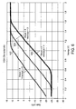
- the gain with a slope of 15 and intercept of 2 is shown at 116.
- the gain with a slope of 8 and intercept of 2 is shown at 118.
- the gain with a slope of 0 and intercept of 2 is shown at 120.
- Figure 6 shows a similar set of gain relationships.
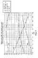
- the gain with a slope of 8 and intercept of 0 is shown at 122.
- the gain with a slope of 8 and intercept of 2 is shown at 124, and the gain with a slope of 8 and intercept of 4 is shown at 126 for a system in accordance with an embodiment of the invention.
- Figure 7 shows the variable gain amplifier gain 128, the log-detector gain 130, the power amplifier gain 132, and the loop gain 134.
- the use of the programmable VGA allows the overall loop gain 134 to remain relatively constant over output power, despite the variations in both the log-detector gain and the power amplifier gain.
- This constant loop gain translates into constant loop bandwidth (and corresponding delay) and therefore facilitates easy time-alignment with a phase loop that similarly has constant delay over output power.
Landscapes
- Engineering & Computer Science (AREA)
- Power Engineering (AREA)
- Computer Networks & Wireless Communication (AREA)
- Signal Processing (AREA)
- Physics & Mathematics (AREA)
- Nonlinear Science (AREA)
- Transmitters (AREA)
- Amplifiers (AREA)
- Radar Systems Or Details Thereof (AREA)
Claims (13)
- Circuit d'émetteur destiné à être utilisé dans un système de communication sans fil multifréquence, ledit circuit d'émetteur comprenant :une unité de modulation d'entrée (10 ; 30) pour recevoir au moins un signal qui est représentatif d'une information devant être modulée ;un système de modulation de phase (12, 14, 20, 22 ; 32, 34, 36, 40, 64, 66) couplé à la sortie de l'unité de modulation d'entrée (10 ; 30) pour réaliser une modulation de phase sur un signal de sortie (VOUT), ledit système de modulation de phase (12, 14, 20, 22 ; 32, 34, 36, 40, 64, 66) comprenant un système de détection de phase (12 ; 32) et un amplificateur de puissance réglable (14 ; 40) ; etun système de modulation d'amplitude (18) pour réaliser une modulation d'amplitude sur le signal de sortie, caractérisé en ce que :le système de modulation d'amplitude (18) est couplé de façon à recevoir la sortie de l'unité de modulation d'entrée (10 ; 30) et la sortie de l'amplificateur de puissance réglable (14 ; 40), et comprend un système de détection d'amplitude comprenant un amplificateur à gain variable (58) couplé de façon à recevoir un signal d'erreur (Verr) dérivé de la sortie de l'unité de modulation d'entrée (10 ; 30) et de la sortie de l'amplificateur de puissance réglable (14 ; 40), le gain de l'amplificateur à gain variable étant commandé à l'aide d'une tension en rampe (VRAMP) associée à la puissance de sortie de l'amplificateur de puissance réglable, et l'amplificateur à gain variable délivrant un signal de commande (VAPC) pour commander l'amplificateur de puissance réglable afin d'assurer un alignement dans le temps substantiel des signaux d'amplitude et de phase sur une plage de fonctionnement de niveaux de puissance.
- Emetteur selon la revendication 1, dans lequel ledit système de modulation d'amplitude comprend au moins un amplificateur logarithmique (44, 46).
- Emetteur selon la revendication 2, dans lequel ledit amplificateur logarithmique (44) est couplé de façon à recevoir le signal de sortie.
- Emetteur selon la revendication 1, dans lequel le système de détection d'amplitude comprend un amplificateur d'intégration (60) qui est couplé à la sortie de l'amplificateur à gain variable (58).
- Emetteur selon la revendication 1, dans lequel ledit amplificateur à gain variable (58) reçoit des données d'entrée concernant le gain.
- Emetteur selon la revendication 1, dans lequel ledit amplificateur à gain variable reçoit des données d'entrée concernant la pente et l'interception.
- Emetteur selon la revendication 1, dans lequel ledit signal en rampe d'entrée est proportionnel au logarithme de la tension de sortie.
- Emetteur selon la revendication 1, dans lequel le signal de sortie est couplé au système de modulation d'amplitude (18) par l'intermédiaire d'un premier amplificateur logarithmique (44), et l'unité de modulation d'entrée (10 ; 30) est couplée au système de modulation d'amplitude (18) par l'intermédiaire d'un deuxième amplificateur logarithmique (46).
- Emetteur selon la revendication 1, dans lequel le système de modulation d'amplitude comprend un amplificateur de suivi et de maintien (54).
- Circuit d'émetteur selon l'une quelconque des revendications 1 à 10, dans lequel l'unité de modulation d'entrée comprend une unité de modulation en quadrature pour recevoir des signaux d'entrée I et Q qui sont représentatifs d'une information devant être modulée.
- Procédé pour générer un signal de sortie dans un circuit d'émetteur destiné à être utilisé dans un système de communication sans fil multifréquence, ledit procédé comprenant les étapes consistant à :recevoir dans une unité de modulation au moins un signal qui est représentatif d'une information devant être modulée ;réaliser une modulation de phase sur le signal de sortie à l'aide d'une boucle à verrouillage de phase et d'un amplificateur de puissance réglable ; etréaliser une modulation d'amplitude sur le signal de sortie à l'aide d'un système de modulation d'amplitude ; caractérisé par les étapes consistant à :recevoir la sortie de l'unité de modulation et la sortie de l'amplificateur de puissance réglable dans un système de détection d'amplitude comprenant un amplificateur à gain variable, et déterminer un signal d'erreur en fonction des sorties reçues ;amplifier le signal d'erreur à l'aide d'un amplificateur à gain variable, le gain de l'amplificateur à gain variable étant déterminé par une tension en rampe (VRAMP), la tension en rampe (VRAMP) étant associée à la puissance de sortie de l'amplificateur de puissance réglable ; etcommander l'amplificateur de puissance réglable à l'aide de la sortie de l'amplificateur à gain variable afin d'assurer un alignement dans le temps substantiel des signaux d'amplitude et de phase sur une plage de fonctionnement de niveaux de puissance.
- Procédé selon la revendication 11, dans lequel ledit système de modulation d'amplitude comprend au moins un amplificateur logarithmique.
- Procédé selon la revendication 11, dans lequel le système de détection d'amplitude comprend un amplificateur d'intégration qui est couplé à la sortie de l'amplificateur à gain variable.
Applications Claiming Priority (2)
| Application Number | Priority Date | Filing Date | Title |
|---|---|---|---|
| US11/450,115 US7558542B2 (en) | 2006-06-09 | 2006-06-09 | System and method for providing a transmitter for polar modulation and power amplifier linearization |
| PCT/US2007/070473 WO2007146691A2 (fr) | 2006-06-09 | 2007-06-06 | Système et procédé pour constituer un circuit émetteur pour une modulation polaire et une linéarisation d'amplificateur de puissance |
Publications (2)
| Publication Number | Publication Date |
|---|---|
| EP2027649A2 EP2027649A2 (fr) | 2009-02-25 |
| EP2027649B1 true EP2027649B1 (fr) | 2010-11-17 |
Family
ID=38822560
Family Applications (1)
| Application Number | Title | Priority Date | Filing Date |
|---|---|---|---|
| EP07812024A Not-in-force EP2027649B1 (fr) | 2006-06-09 | 2007-06-06 | Système et procédé pour constituer un circuit émetteur pour une modulation polaire et une linéarisation d'amplificateur de puissance |
Country Status (6)
| Country | Link |
|---|---|
| US (1) | US7558542B2 (fr) |
| EP (1) | EP2027649B1 (fr) |
| CN (1) | CN101361264B (fr) |
| AT (1) | ATE488909T1 (fr) |
| DE (1) | DE602007010617D1 (fr) |
| WO (1) | WO2007146691A2 (fr) |
Families Citing this family (28)
| Publication number | Priority date | Publication date | Assignee | Title |
|---|---|---|---|---|
| GB2389253B (en) * | 2002-05-31 | 2005-09-21 | Hitachi Ltd | Transmitter and semiconductor integrated circuit for communication |
| US8301086B2 (en) * | 2002-10-04 | 2012-10-30 | Quintic Holdings | Low-power polar transmitter |
| US7917106B2 (en) * | 2006-02-03 | 2011-03-29 | Quantance, Inc. | RF power amplifier controller circuit including calibrated phase control loop |
| US8032097B2 (en) * | 2006-02-03 | 2011-10-04 | Quantance, Inc. | Amplitude error de-glitching circuit and method of operating |
| US7697903B2 (en) * | 2006-12-06 | 2010-04-13 | Broadcom Corporation | Method and system for level detector calibration for accurate transmit power control |
| US7729671B2 (en) * | 2006-12-06 | 2010-06-01 | Broadcom Corporation | Method and system for enhancing efficiency by modulating power amplifier gain |
| US7890067B2 (en) * | 2007-05-10 | 2011-02-15 | Pine Valley Investments, Inc. | Linear RF amplifier with polar feedback |
| JP4757231B2 (ja) * | 2007-06-01 | 2011-08-24 | 富士通株式会社 | 送信装置 |
| US8995567B2 (en) * | 2007-07-31 | 2015-03-31 | Broadcom Corporation | Method and system for power supply adjustment and polar modulation in a MIMO system |
| US8442456B2 (en) * | 2007-08-09 | 2013-05-14 | Freescale Semiconductor, Inc. | Wireless communication unit, integrated circuit and method of power control therein |
| US7805116B2 (en) * | 2007-09-28 | 2010-09-28 | Freescale Semiconductor, Inc. | Gain control methods for wireless devices and transmitters |
| US8781536B1 (en) | 2008-03-06 | 2014-07-15 | Marvell International Ltd | Power control using fast signal correlation |
| US8099139B1 (en) | 2008-03-06 | 2012-01-17 | Marvell International Ltd. | Power control using fast signal envelope detection |
| US8463207B2 (en) * | 2008-08-20 | 2013-06-11 | Freescale Semiconductor, Inc. | Wireless communication unit, integrated circuit and method of power control of a power amplifier therefor |
| US8022734B1 (en) | 2008-08-25 | 2011-09-20 | Peregrine Semiconductor Corporation | Low current power detection circuit providing window comparator functionality |
| US8644776B1 (en) | 2008-08-25 | 2014-02-04 | Peregrine Semiconductor Corporation | Systems and methods for providing improved power performance in wireless communication systems |
| US8433263B2 (en) * | 2008-09-24 | 2013-04-30 | Freescale Semiconductor, Inc. | Wireless communication unit, integrated circuit and method of power control of a power amplifier therefor |
| US8666325B2 (en) | 2008-12-03 | 2014-03-04 | Intel Mobile Communications GmbH | Polar feedback receiver for modulator |
| CN102577101A (zh) * | 2009-08-27 | 2012-07-11 | 京瓷株式会社 | 检波装置及使用了它的放大装置、发送装置和通信装置 |
| EP2346175B1 (fr) * | 2010-01-15 | 2015-03-11 | Telefonaktiebolaget L M Ericsson | Procédé et dispositifs de transmission pour configurer un amplificateur de puissance multisupport |
| US9432946B2 (en) * | 2012-03-12 | 2016-08-30 | Nec Corporation | Transmission apparatus and transmission method |
| WO2014081738A1 (fr) | 2012-11-21 | 2014-05-30 | Marvell World Trade Ltd. | Procédé pour une commande de puissance automatique rapide d'émetteurs sans fil |
| US8824981B2 (en) * | 2013-01-31 | 2014-09-02 | Intel Mobile Communications GmbH | Recalibration of envelope tracking transfer function during active transmission |
| CN105897201B (zh) * | 2016-03-31 | 2019-01-25 | 宜确半导体(苏州)有限公司 | 一种gsm射频功率放大器 |
| CN106992757A (zh) * | 2017-04-07 | 2017-07-28 | 宜确半导体(苏州)有限公司 | 一种射频功率放大器电路 |
| CN112148052B (zh) * | 2020-09-28 | 2022-10-11 | 刘承鑫 | 一种便携式可调的稳定交流高压产生系统 |
| US11463059B1 (en) * | 2021-03-23 | 2022-10-04 | Marvell Asia Pte Ltd. | Systems and methods for linear variable gain amplifier |
| CN119997184B (zh) * | 2025-04-09 | 2025-06-20 | 四川创智联恒科技有限公司 | 一种基站接收链路的增益控制方法、程序产品、电子设备及存储介质 |
Family Cites Families (10)
| Publication number | Priority date | Publication date | Assignee | Title |
|---|---|---|---|---|
| CN1252910C (zh) * | 2000-10-17 | 2006-04-19 | 艾利森电话股份有限公司 | 通信系统 |
| US6801784B1 (en) | 2000-11-02 | 2004-10-05 | Skyworks Solutions, Inc. | Continuous closed-loop power control system including modulation injection in a wireless transceiver power amplifier |
| GB2369941A (en) | 2000-12-09 | 2002-06-12 | Roke Manor Research | A polar loop amplifier arrangement with variable gain in a feedback loop |
| US7409004B2 (en) * | 2001-06-19 | 2008-08-05 | Matsushita Electric Industrial Co., Ltd. | Hybrid polar modulator differential phase Cartesian feedback correction circuit for power amplifier linearization |
| GB2380880B (en) | 2001-10-10 | 2004-02-11 | Zarlink Semiconductor Ltd | A polar loop transmitter |
| EP2284996A1 (fr) * | 2003-03-12 | 2011-02-16 | MediaTek Inc. | Contrôle de la puissance en boucle fermée de formes d'ondes à enveloppe non constante utilisant un échantillon/maintien |
| US7072626B2 (en) * | 2003-04-30 | 2006-07-04 | Telefonaktiebolaget Lm Ericsson (Publ) | Polar modulation transmitter |
| JP2005072031A (ja) * | 2003-08-22 | 2005-03-17 | Renesas Technology Corp | 高周波用半導体装置および通信用電子部品並びに無線通信システム |
| US7460842B2 (en) * | 2005-09-08 | 2008-12-02 | Motorola, Inc. | Wireless transmitter having polar loop controller with current feedback and methods |
| US7518445B2 (en) * | 2006-06-04 | 2009-04-14 | Samsung Electro-Mechanics Company, Ltd. | Systems, methods, and apparatuses for linear envelope elimination and restoration transmitters |
-
2006
- 2006-06-09 US US11/450,115 patent/US7558542B2/en active Active
-
2007
- 2007-06-06 CN CN2007800015325A patent/CN101361264B/zh not_active Expired - Fee Related
- 2007-06-06 EP EP07812024A patent/EP2027649B1/fr not_active Not-in-force
- 2007-06-06 DE DE602007010617T patent/DE602007010617D1/de active Active
- 2007-06-06 AT AT07812024T patent/ATE488909T1/de not_active IP Right Cessation
- 2007-06-06 WO PCT/US2007/070473 patent/WO2007146691A2/fr not_active Ceased
Also Published As
| Publication number | Publication date |
|---|---|
| US20070287393A1 (en) | 2007-12-13 |
| ATE488909T1 (de) | 2010-12-15 |
| CN101361264B (zh) | 2011-08-10 |
| WO2007146691A2 (fr) | 2007-12-21 |
| US7558542B2 (en) | 2009-07-07 |
| CN101361264A (zh) | 2009-02-04 |
| EP2027649A2 (fr) | 2009-02-25 |
| DE602007010617D1 (de) | 2010-12-30 |
| WO2007146691A3 (fr) | 2008-04-24 |
Similar Documents
| Publication | Publication Date | Title |
|---|---|---|
| EP2027649B1 (fr) | Système et procédé pour constituer un circuit émetteur pour une modulation polaire et une linéarisation d'amplificateur de puissance | |
| KR100701913B1 (ko) | 무선 트랜시버 전력 증폭기로의 변조 주입을 포함하는연속 폐루프 전력 제어 시스템 | |
| US7783269B2 (en) | Power amplifier controller with polar transmitter | |
| US7072420B2 (en) | Communications systems | |
| US7062236B2 (en) | Transmitter circuits | |
| US6868279B2 (en) | Power characteristic of a radio transmitter | |
| JP3698669B2 (ja) | 極ループ送信回路 | |
| US20040235437A1 (en) | Closed loop power control of non-constant envelope waveforms using sample/hold | |
| US6968163B2 (en) | Method and transmission circuit for generating a transmission signal | |
| AU1048400A (en) | Method and arrangement for correcting phase error in linearization loop of power amplifier | |
| WO2008054673A1 (fr) | Système et procédé d'étalonnage de régulation de puissance en circuit fermé | |
| US20050078768A1 (en) | Adaptive phase controller, method of controlling a phase and transmitter employing the same | |
| EP1415410B1 (fr) | Commande de regulation pour une modulation d'enveloppe non constante | |
| US8964892B2 (en) | Apparatus and method for operating a transmitter | |
| WO1992008297A1 (fr) | Appareil et methode servant a modifier un signal dans l'emetteur d'un emetteur-recepteur | |
| US6731915B1 (en) | Combined RF power detector and power precorrector | |
| US9853608B2 (en) | Temperature compensation technique for envelope tracking system | |
| US6904268B2 (en) | Low noise linear transmitter using cartesian feedback | |
| US20020009981A1 (en) | Power control method and power control system | |
| CN1711696B (zh) | 传输级 | |
| EP1936898A1 (fr) | Dispositif de communication sans fil et dispositif de modulation de phase | |
| JPH0758568A (ja) | 送信出力自動制御方式 |
Legal Events
| Date | Code | Title | Description |
|---|---|---|---|
| PUAI | Public reference made under article 153(3) epc to a published international application that has entered the european phase |
Free format text: ORIGINAL CODE: 0009012 |
|
| 17P | Request for examination filed |
Effective date: 20080702 |
|
| AK | Designated contracting states |
Kind code of ref document: A2 Designated state(s): AT BE BG CH CY CZ DE DK EE ES FI FR GB GR HU IE IS IT LI LT LU LV MC MT NL PL PT RO SE SI SK TR |
|
| AX | Request for extension of the european patent |
Extension state: AL BA HR MK RS |
|
| RAP1 | Party data changed (applicant data changed or rights of an application transferred) |
Owner name: MEDIATEK, INC |
|
| 17Q | First examination report despatched |
Effective date: 20090624 |
|
| DAX | Request for extension of the european patent (deleted) | ||
| GRAP | Despatch of communication of intention to grant a patent |
Free format text: ORIGINAL CODE: EPIDOSNIGR1 |
|
| GRAS | Grant fee paid |
Free format text: ORIGINAL CODE: EPIDOSNIGR3 |
|
| GRAA | (expected) grant |
Free format text: ORIGINAL CODE: 0009210 |
|
| AK | Designated contracting states |
Kind code of ref document: B1 Designated state(s): AT BE BG CH CY CZ DE DK EE ES FI FR GB GR HU IE IS IT LI LT LU LV MC MT NL PL PT RO SE SI SK TR |
|
| REG | Reference to a national code |
Ref country code: GB Ref legal event code: FG4D |
|
| REG | Reference to a national code |
Ref country code: CH Ref legal event code: EP |
|
| REG | Reference to a national code |
Ref country code: IE Ref legal event code: FG4D |
|
| REF | Corresponds to: |
Ref document number: 602007010617 Country of ref document: DE Date of ref document: 20101230 Kind code of ref document: P |
|
| REG | Reference to a national code |
Ref country code: NL Ref legal event code: VDEP Effective date: 20101117 |
|
| LTIE | Lt: invalidation of european patent or patent extension |
Effective date: 20101117 |
|
| PG25 | Lapsed in a contracting state [announced via postgrant information from national office to epo] |
Ref country code: LT Free format text: LAPSE BECAUSE OF FAILURE TO SUBMIT A TRANSLATION OF THE DESCRIPTION OR TO PAY THE FEE WITHIN THE PRESCRIBED TIME-LIMIT Effective date: 20101117 |
|
| PG25 | Lapsed in a contracting state [announced via postgrant information from national office to epo] |
Ref country code: LV Free format text: LAPSE BECAUSE OF FAILURE TO SUBMIT A TRANSLATION OF THE DESCRIPTION OR TO PAY THE FEE WITHIN THE PRESCRIBED TIME-LIMIT Effective date: 20101117 Ref country code: NL Free format text: LAPSE BECAUSE OF FAILURE TO SUBMIT A TRANSLATION OF THE DESCRIPTION OR TO PAY THE FEE WITHIN THE PRESCRIBED TIME-LIMIT Effective date: 20101117 Ref country code: IS Free format text: LAPSE BECAUSE OF FAILURE TO SUBMIT A TRANSLATION OF THE DESCRIPTION OR TO PAY THE FEE WITHIN THE PRESCRIBED TIME-LIMIT Effective date: 20110317 Ref country code: SI Free format text: LAPSE BECAUSE OF FAILURE TO SUBMIT A TRANSLATION OF THE DESCRIPTION OR TO PAY THE FEE WITHIN THE PRESCRIBED TIME-LIMIT Effective date: 20101117 Ref country code: CY Free format text: LAPSE BECAUSE OF FAILURE TO SUBMIT A TRANSLATION OF THE DESCRIPTION OR TO PAY THE FEE WITHIN THE PRESCRIBED TIME-LIMIT Effective date: 20101117 Ref country code: AT Free format text: LAPSE BECAUSE OF FAILURE TO SUBMIT A TRANSLATION OF THE DESCRIPTION OR TO PAY THE FEE WITHIN THE PRESCRIBED TIME-LIMIT Effective date: 20101117 Ref country code: BG Free format text: LAPSE BECAUSE OF FAILURE TO SUBMIT A TRANSLATION OF THE DESCRIPTION OR TO PAY THE FEE WITHIN THE PRESCRIBED TIME-LIMIT Effective date: 20110217 Ref country code: PT Free format text: LAPSE BECAUSE OF FAILURE TO SUBMIT A TRANSLATION OF THE DESCRIPTION OR TO PAY THE FEE WITHIN THE PRESCRIBED TIME-LIMIT Effective date: 20110317 Ref country code: SE Free format text: LAPSE BECAUSE OF FAILURE TO SUBMIT A TRANSLATION OF THE DESCRIPTION OR TO PAY THE FEE WITHIN THE PRESCRIBED TIME-LIMIT Effective date: 20101117 |
|
| PG25 | Lapsed in a contracting state [announced via postgrant information from national office to epo] |
Ref country code: GR Free format text: LAPSE BECAUSE OF FAILURE TO SUBMIT A TRANSLATION OF THE DESCRIPTION OR TO PAY THE FEE WITHIN THE PRESCRIBED TIME-LIMIT Effective date: 20110218 |
|
| PG25 | Lapsed in a contracting state [announced via postgrant information from national office to epo] |
Ref country code: ES Free format text: LAPSE BECAUSE OF FAILURE TO SUBMIT A TRANSLATION OF THE DESCRIPTION OR TO PAY THE FEE WITHIN THE PRESCRIBED TIME-LIMIT Effective date: 20110228 Ref country code: EE Free format text: LAPSE BECAUSE OF FAILURE TO SUBMIT A TRANSLATION OF THE DESCRIPTION OR TO PAY THE FEE WITHIN THE PRESCRIBED TIME-LIMIT Effective date: 20101117 Ref country code: CZ Free format text: LAPSE BECAUSE OF FAILURE TO SUBMIT A TRANSLATION OF THE DESCRIPTION OR TO PAY THE FEE WITHIN THE PRESCRIBED TIME-LIMIT Effective date: 20101117 Ref country code: BE Free format text: LAPSE BECAUSE OF FAILURE TO SUBMIT A TRANSLATION OF THE DESCRIPTION OR TO PAY THE FEE WITHIN THE PRESCRIBED TIME-LIMIT Effective date: 20101117 |
|
| PG25 | Lapsed in a contracting state [announced via postgrant information from national office to epo] |
Ref country code: PL Free format text: LAPSE BECAUSE OF FAILURE TO SUBMIT A TRANSLATION OF THE DESCRIPTION OR TO PAY THE FEE WITHIN THE PRESCRIBED TIME-LIMIT Effective date: 20101117 Ref country code: RO Free format text: LAPSE BECAUSE OF FAILURE TO SUBMIT A TRANSLATION OF THE DESCRIPTION OR TO PAY THE FEE WITHIN THE PRESCRIBED TIME-LIMIT Effective date: 20101117 Ref country code: DK Free format text: LAPSE BECAUSE OF FAILURE TO SUBMIT A TRANSLATION OF THE DESCRIPTION OR TO PAY THE FEE WITHIN THE PRESCRIBED TIME-LIMIT Effective date: 20101117 Ref country code: SK Free format text: LAPSE BECAUSE OF FAILURE TO SUBMIT A TRANSLATION OF THE DESCRIPTION OR TO PAY THE FEE WITHIN THE PRESCRIBED TIME-LIMIT Effective date: 20101117 |
|
| PLBE | No opposition filed within time limit |
Free format text: ORIGINAL CODE: 0009261 |
|
| STAA | Information on the status of an ep patent application or granted ep patent |
Free format text: STATUS: NO OPPOSITION FILED WITHIN TIME LIMIT |
|
| 26N | No opposition filed |
Effective date: 20110818 |
|
| REG | Reference to a national code |
Ref country code: DE Ref legal event code: R097 Ref document number: 602007010617 Country of ref document: DE Effective date: 20110818 |
|
| PG25 | Lapsed in a contracting state [announced via postgrant information from national office to epo] |
Ref country code: MT Free format text: LAPSE BECAUSE OF FAILURE TO SUBMIT A TRANSLATION OF THE DESCRIPTION OR TO PAY THE FEE WITHIN THE PRESCRIBED TIME-LIMIT Effective date: 20101117 |
|
| REG | Reference to a national code |
Ref country code: CH Ref legal event code: PL |
|
| REG | Reference to a national code |
Ref country code: IE Ref legal event code: MM4A |
|
| PG25 | Lapsed in a contracting state [announced via postgrant information from national office to epo] |
Ref country code: LI Free format text: LAPSE BECAUSE OF NON-PAYMENT OF DUE FEES Effective date: 20110630 Ref country code: IE Free format text: LAPSE BECAUSE OF NON-PAYMENT OF DUE FEES Effective date: 20110606 Ref country code: CH Free format text: LAPSE BECAUSE OF NON-PAYMENT OF DUE FEES Effective date: 20110630 |
|
| PG25 | Lapsed in a contracting state [announced via postgrant information from national office to epo] |
Ref country code: MC Free format text: LAPSE BECAUSE OF NON-PAYMENT OF DUE FEES Effective date: 20110630 |
|
| PG25 | Lapsed in a contracting state [announced via postgrant information from national office to epo] |
Ref country code: LU Free format text: LAPSE BECAUSE OF NON-PAYMENT OF DUE FEES Effective date: 20110606 |
|
| PG25 | Lapsed in a contracting state [announced via postgrant information from national office to epo] |
Ref country code: TR Free format text: LAPSE BECAUSE OF FAILURE TO SUBMIT A TRANSLATION OF THE DESCRIPTION OR TO PAY THE FEE WITHIN THE PRESCRIBED TIME-LIMIT Effective date: 20101117 |
|
| PG25 | Lapsed in a contracting state [announced via postgrant information from national office to epo] |
Ref country code: HU Free format text: LAPSE BECAUSE OF FAILURE TO SUBMIT A TRANSLATION OF THE DESCRIPTION OR TO PAY THE FEE WITHIN THE PRESCRIBED TIME-LIMIT Effective date: 20101117 |
|
| REG | Reference to a national code |
Ref country code: FR Ref legal event code: PLFP Year of fee payment: 10 |
|
| REG | Reference to a national code |
Ref country code: FR Ref legal event code: PLFP Year of fee payment: 11 |
|
| REG | Reference to a national code |
Ref country code: FR Ref legal event code: PLFP Year of fee payment: 12 |
|
| P01 | Opt-out of the competence of the unified patent court (upc) registered |
Effective date: 20230607 |
|
| PGFP | Annual fee paid to national office [announced via postgrant information from national office to epo] |
Ref country code: FR Payment date: 20230626 Year of fee payment: 17 Ref country code: DE Payment date: 20230626 Year of fee payment: 17 |
|
| PGFP | Annual fee paid to national office [announced via postgrant information from national office to epo] |
Ref country code: FI Payment date: 20230626 Year of fee payment: 17 |
|
| PGFP | Annual fee paid to national office [announced via postgrant information from national office to epo] |
Ref country code: IT Payment date: 20230620 Year of fee payment: 17 Ref country code: GB Payment date: 20230627 Year of fee payment: 17 |
|
| REG | Reference to a national code |
Ref country code: DE Ref legal event code: R119 Ref document number: 602007010617 Country of ref document: DE |
|
| PG25 | Lapsed in a contracting state [announced via postgrant information from national office to epo] |
Ref country code: FI Free format text: LAPSE BECAUSE OF NON-PAYMENT OF DUE FEES Effective date: 20240606 |
|
| PG25 | Lapsed in a contracting state [announced via postgrant information from national office to epo] |
Ref country code: FI Free format text: LAPSE BECAUSE OF NON-PAYMENT OF DUE FEES Effective date: 20240606 |
|
| GBPC | Gb: european patent ceased through non-payment of renewal fee |
Effective date: 20240606 |
|
| PG25 | Lapsed in a contracting state [announced via postgrant information from national office to epo] |
Ref country code: DE Free format text: LAPSE BECAUSE OF NON-PAYMENT OF DUE FEES Effective date: 20250101 |
|
| PG25 | Lapsed in a contracting state [announced via postgrant information from national office to epo] |
Ref country code: FR Free format text: LAPSE BECAUSE OF NON-PAYMENT OF DUE FEES Effective date: 20240630 |
|
| PG25 | Lapsed in a contracting state [announced via postgrant information from national office to epo] |
Ref country code: GB Free format text: LAPSE BECAUSE OF NON-PAYMENT OF DUE FEES Effective date: 20240606 Ref country code: IT Free format text: LAPSE BECAUSE OF NON-PAYMENT OF DUE FEES Effective date: 20240606 |