EP2028660B1 - Taktsignalerzeuger zur Erzeugung von stabilen Taktsignalen, Halbleiterspeichervorrichtung damit und Bedienungsverfahren - Google Patents
Taktsignalerzeuger zur Erzeugung von stabilen Taktsignalen, Halbleiterspeichervorrichtung damit und Bedienungsverfahren Download PDFInfo
- Publication number
- EP2028660B1 EP2028660B1 EP08252615.3A EP08252615A EP2028660B1 EP 2028660 B1 EP2028660 B1 EP 2028660B1 EP 08252615 A EP08252615 A EP 08252615A EP 2028660 B1 EP2028660 B1 EP 2028660B1
- Authority
- EP
- European Patent Office
- Prior art keywords
- clock signal
- pulses
- host
- memory device
- semiconductor memory
- Prior art date
- Legal status (The legal status is an assumption and is not a legal conclusion. Google has not performed a legal analysis and makes no representation as to the accuracy of the status listed.)
- Active
Links
Images

Classifications
-
- H—ELECTRICITY
- H04—ELECTRIC COMMUNICATION TECHNIQUE
- H04L—TRANSMISSION OF DIGITAL INFORMATION, e.g. TELEGRAPHIC COMMUNICATION
- H04L7/00—Arrangements for synchronising receiver with transmitter
- H04L7/04—Speed or phase control by synchronisation signals
- H04L7/08—Speed or phase control by synchronisation signals the synchronisation signals recurring cyclically
-
- G—PHYSICS
- G06—COMPUTING OR CALCULATING; COUNTING
- G06F—ELECTRIC DIGITAL DATA PROCESSING
- G06F1/00—Details not covered by groups G06F3/00 - G06F13/00 and G06F21/00
- G06F1/04—Generating or distributing clock signals or signals derived directly therefrom
- G06F1/08—Clock generators with changeable or programmable clock frequency
-
- G—PHYSICS
- G11—INFORMATION STORAGE
- G11C—STATIC STORES
- G11C7/00—Arrangements for writing information into, or reading information out from, a digital store
- G11C7/22—Read-write [R-W] timing or clocking circuits; Read-write [R-W] control signal generators or management
-
- G—PHYSICS
- G11—INFORMATION STORAGE
- G11C—STATIC STORES
- G11C7/00—Arrangements for writing information into, or reading information out from, a digital store
- G11C7/22—Read-write [R-W] timing or clocking circuits; Read-write [R-W] control signal generators or management
- G11C7/222—Clock generating, synchronizing or distributing circuits within memory device
-
- H—ELECTRICITY
- H03—ELECTRONIC CIRCUITRY
- H03L—AUTOMATIC CONTROL, STARTING, SYNCHRONISATION OR STABILISATION OF GENERATORS OF ELECTRONIC OSCILLATIONS OR PULSES
- H03L7/00—Automatic control of frequency or phase; Synchronisation
- H03L7/06—Automatic control of frequency or phase; Synchronisation using a reference signal applied to a frequency- or phase-locked loop
- H03L7/08—Details of the phase-locked loop
- H03L7/085—Details of the phase-locked loop concerning mainly the frequency- or phase-detection arrangement including the filtering or amplification of its output signal
Definitions
- the present invention relates to a semiconductor memory device, and more particularly, to a semiconductor memory device including a clock signal generator for generating a stable clock signal and method thereof.
- a host can generate a stable clock signal used during data communication with a smart card and can thus generate a stable clock signal in the different communication modes of the USB.
- the clock signal may be unstable. For example, even if the smart card locks onto the clock signal, the clock signal may be unstable due to environmental facts such as temperature and voltage of the smart card.
- US 2005/0081076 discloses a semiconductor integrated circuit provided with an external interface circuit, which includes a clock generation circuit for generating a synchronous clock signal to establish synchronization between data input and output through a data string sectioned at fixed intervals.
- US 2003/0086518 discloses a method and an improved apparatus for clock recovery from data streams containing embedded reference clock values controlled clock source means includes of a controllable digital fractional divider means receiving a control value from digital comparator means and a clock input from a digital clock synthesizer means driven by a fixed oscillator means.
- Embodiments according to the invention can provide clock signal generator for generating stable clock signals, semiconductor memory device including the same, and methods of operating.
- a clock signal generator can include a clock signal generation unit that is configured to generate a clock signal.
- a clock signal control unit is configured to count a number of pulses of the clock signal during a reference time, and to compare the number of pulses with a reference value to provide a comparison result, and to generate a control signal based on the comparison result, where the clock signal generation unit increases or decreases the number of pulses of the clock signal, based on the control signal.
- first, second, etc. may be used herein to describe various elements, these elements should not be limited by these terms. These terms are only used to distinguish one element from another. For example, a first signal could be termed a second signal, and, similarly, a second signal could be termed a first signal without departing from the teachings of the disclosure.
- FIG. 1 is a block diagram of a semiconductor memory device 14 according to some embodiments of the present invention.
- FIG. 2 illustrates a transmission frame structure in which the semiconductor memory device 14 illustrated in FIG. 1 receives data from a host 13.
- the semiconductor memory device 14 may include a central processing unit (CPU) 16 and a clock signal generator 18.
- the CPU 16 and the clock signal generator 18 may be implemented on a single chip.
- the semiconductor memory device 14 may be at least one of a smart card and an S-subscriber identification module (S-SIM) card or may be a CompactFlash (CF) card, a memory stick, a memory stick duo, a multimedia card (MMC), a reduced-size MMC, a secure digital (SD) card, a miniSD card, a microSD (or TransFlash) card, or an XD-picture card.
- S-SIM S-subscriber identification module
- CF CompactFlash
- MMC multimedia card
- SD secure digital
- miniSD miniSD
- microSD microSD
- XD-picture card XD-picture card
- the CPU 16 transmits data to and receives data from the host 13 through a universal serial bus (USB) 12 based on a clock signal CLK generated by the clock signal generator 18 (sometimes referred to as the clock signal generator circuit).
- the USB 12 may be implemented by a four-wire cable and transfer a signal or a frame ( FIG. 2 ) and power between the host 13 and the CPU 16.
- the USB 12 may transmit power from the host 13 to the semiconductor memory device 14 through two power supply lines (not shown) and transfer a signal (or a frame) between the host 13 and the CPU 16 through two signal lines (not shown).
- the host 13 may be a personal computer (PC), a video camera, a television, an MP3 player, a game, an electronic instrument, a mobile terminal, a personal digital assistant (PDA), a voice recorder, or a notebook computer.
- PC personal computer
- PDA personal digital assistant
- the clock signal generator 18 generates the clock signal CLK, counts the number of pulses of the clock signal CLK during a reference time, compares a result of the counting with a reference value 25, and increases or decreases the number of pulses of the clock signal CLK based on a result of the comparison. In some embodiments according to the invention, the number of pulses of the clock signal CLK generated during the reference time is increased or decreased based on the comparison result.
- the reference time may be determined based on a signal periodically generated by the host 13.
- the reference time may be a period of time from reception of a first start-of-frame (SOF) signal 31 sent by the host 13 through the USB 12 to reception of a second SOF signal 35 sent after the first SOF signal 31, but the present invention is not restricted thereto.
- SOF start-of-frame
- the clock signal generator 18 may detect the reference time based on the SOF signals 31 and 35 and count the number of pulses of the clock signal CLK during the detected reference time.
- the clock signal generator 18 may include a clock signal control unit 20 and a clock signal generation unit 28.
- the clock signal control unit 20 counts the number of pulses of the clock signal CLK during the reference time, compares a counting result CNT with the reference value 25, and generates a control signal C-signal based on a comparison result CR.
- the clock signal control unit 20 may include a counter 22, a comparator 24, and a controller 26.
- the counter 22 counts the number of pulses of the clock signal CLK during the reference time. For instance, the counter 22 starts counting the number of pulses of the clock signal CLK in response to the first SOF signal 31 received from the CPU 16 and is then reset in response to the second SOF signal 35 received after the first SOF signal 31, thereby outputting the counting result CNT.
- the comparator 24 compares the counting result CNT received from the counter 22 with the reference value 25 and outputs the comparison result CR.
- the controller 26 outputs the control signal C-signal for increasing or decreasing the number of pulses of the clock signal CLK based on the comparison result CR.
- the reference value 25 indicates the number of pulses of a clock signal referred to when data is transferred between the host 13 and the CPU 16 through the USB 12 and may be input by a user and stored at a storage (not shown) included in the comparator 24 through a user interface (not shown) or may be received from the host 13 through the CPU 16 and stored at the storage (not shown) of the comparator 24. For instance, when the reference value 25 is 48,000, the comparator 24 compares the counting result CNT with the value of 48,000.
- the controller 26 may output the control signal C-signal for maintaining the number of pulses of the clock signal CLK to the clock signal generation unit 28 when the counting result CNT is 48,000.
- the controller 26 may output the control signal C-signal for increasing the number of pulses of the clock signal CLK to the clock signal generation unit 28 when the counting result CNT is less than 48,000.
- the controller 26 may output the control signal C-signal for decreasing the number of pulses of the clock signal CLK to the clock signal generation unit 28 when the counting result CNT is greater than 48,000.
- the clock signal generation unit 28 generates the clock signal CLK and increases or decreases the number of pulses of the clock signal CLK in response to the control signal C-signal output from the controller 26.
- the clock signal generation unit 28 may be implemented by a resistor-capacitor (RC) oscillator or a ring oscillator, but the present invention is not restricted thereto.
- RC resistor-capacitor
- a clock signal generated in a conventional semiconductor memory device may be unstable when environmental factors such as internal temperature and voltage of the conventional semiconductor memory device even if it is locked.
- the semiconductor memory device 14 includes the clock signal generator 18 that generates the stable clock signal CLK even when the environmental factors such as temperature and voltage change after the clock signal CLK is locked, thereby allowing efficient data communication with the host 13.
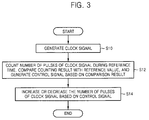
- FIG. 3 is a flowchart of a method of generating a clock signal according to some embodiments of the present invention.
- the clock signal generation unit 28 generates the clock signal CLK in operation S10.
- the clock signal control unit 20 counts the number of pulses of the clock signal CLK during the reference time, compares the counting result CNT with the reference value 25, and generates the control signal C-signal based on the comparison result CR in operation S12.
- the clock signal generation unit 28 increases or decreases the number of pulses of the clock signal CLK based on the control signal C-signal in operation S 14.
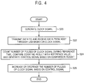
- FIG. 4 is a flowchart of a method of transmitting and receiving data according to some embodiments of the present invention.
- the clock signal generation unit 28 generates the clock signal CLK in operation S20.
- the CPU 16 transmits data to and receives data from the host 13 through the USB 12 based on the clock signal CLK in operation S22.
- the clock signal control unit 20 counts the number of pulses of the clock signal CLK during the reference time, compares the counting result CNT with the reference value 25, and generates the control signal C-signal based on the comparison result CR in operation S24.
- the clock signal generation unit 28 increases or decreases the number of pulses of the clock signal CLK based on the control signal C-signal in operation S26.
- a clock signal generator can generate a stable clock signal regardless of environmental factors such as temperature and voltage.
- a semiconductor memory device includes the clock signal generator that can generate a stable clock signal, thereby performing efficient data communication with a host using the stable clock signal.
Landscapes
- Engineering & Computer Science (AREA)
- Theoretical Computer Science (AREA)
- Physics & Mathematics (AREA)
- General Engineering & Computer Science (AREA)
- General Physics & Mathematics (AREA)
- Computer Networks & Wireless Communication (AREA)
- Signal Processing (AREA)
- Synchronisation In Digital Transmission Systems (AREA)
- Information Transfer Systems (AREA)
- Dram (AREA)
Claims (8)
- Taktsignalerzeuger (18), der Folgendes umfasst:eine Taktsignal-Erzeugungseinheit (28), die dafür konfiguriert ist, ein Taktsignal zu erzeugen, undeine Taktsignal-Steuereinheit (20), die dafür konfiguriert ist, eine Anzahl von Impulsen des während einer Bezugszeit erzeugten Taktsignals zu zählen, die Anzahl von Impulsen mit einem Bezugswert (25) zu vergleichen, um ein Vergleichsergebnis bereitzustellen, und ein Steuersignal auf der Grundlage des Vergleichsergebnisses zu erzeugen, wobeidie Taktsignal-Erzeugungseinheit (28) dafür angeordnet ist, die Anzahl von Impulsen des während einer Bezugszeit erzeugten Taktsignals auf der Grundlage des Steuersignals zu steigern oder zu vermindern, unddie Taktsignal-Erzeugungseinheit (28) einen Speicher umfasst, wobei der Speicher dafür angeordnet ist, den Bezugswert (25) zu speichern, wobei der Bezugswert dafür angeordnet ist, von einem Host (31) empfangen zu werden,dadurch gekennzeichnet, dassdie Bezugszeit ein Zeitraum vom Empfang eines ersten Rahmenbeginnsignals, das von dem Host durch einen Universal Serial Bus übermittelt wird, bis zum Empfang eines zweiten Rahmenbeginnsignals, das von dem Host nach dem ersten Rahmenbeginnsignal übermittelt wird, ist.
- Taktsignalerzeuger (18) nach Anspruch 1, wobei die Taktsignal-Steuereinheit (20) Folgendes umfasst:einen Zähler (22), der dafür konfiguriert ist, die Anzahl von Impulsen des während einer Bezugszeit erzeugten Taktsignals zu zählen,einen Vergleicher (24), der dafür konfiguriert ist, die aus dem Zähler ausgegebene Anzahl von Impulsen mit dem Bezugswert zu vergleichen und das Vergleichsergebnis auszugeben, undein Steuergerät (26), das dafür konfiguriert ist, das Steuersignal zu erzeugen, um die Anzahl von Impulsen des durch die Taktsignal-Erzeugungseinheit (28) erzeugten Taktsignals auf der Grundlage des Vergleichsergebnisses zu steigern oder zu vermindern.
- Verfahren zum Erzeugen eines Taktsignals, wobei das Verfahren Folgendes umfasst:das Erzeugen eines Taktsignals unddas Zählen einer Anzahl von Impulsen des während einer Bezugszeit erzeugten Taktsignals,das Vergleichen der Anzahl von Impulsen mit einem Bezugswert, um ein Vergleichsergebnis bereitzustellen, unddas Erzeugen eines Steuersignals auf der Grundlage des Vergleichsergebnisses, wobei:die Anzahl von Impulsen des während einer Bezugszeit erzeugten Taktsignals auf der Grundlage des Steuersignals gesteigert oder vermindert wird undder Bezugswert von einem Host (31) empfangen und danach in einem Speicher gespeichert wird,dadurch gekennzeichnet, dassdie Bezugszeit ein Zeitraum vom Empfang eines ersten Rahmenbeginnsignals, das von dem Host durch einen Universal Serial Bus übermittelt wird, bis zum Empfang eines zweiten Rahmenbeginnsignals, das von dem Host nach dem ersten Rahmenbeginnsignal übermittelt wird, ist.
- Halbleiter-Speichervorrichtung (14), die Folgendes umfasst:einen Taktsignalerzeuger (18) nach Anspruch 1 oder 2 undeine Zentraleinheit (16), die dafür konfiguriert ist, Daten auf der Grundlage des Taktsignals durch einen Universal Serial Bus zu dem Host (31) zu übermitteln und von demselben zu empfangen.
- Halbleiter-Speichervorrichtung (14) nach Anspruch 4, wobei die Bezugszeit auf der Grundlage eines Rahmenbeginnsignals erfasst wird, das durch den Host (31) erzeugt wird, um einen Beginn eines Rahmens anzuzeigen.
- Halbleiter-Speichervorrichtung (14) nach Anspruch 4, wobei die Halbleiter-Speichervorrichtung (14) wenigstens eines von einer Chipkarte und einer S-Subscriber-Identification-Module- (Teilnehmerkennungsmodul-) (SIM-) Karte ist.
- Verfahren nach Anspruch 3, das Folgendes umfasst:das Übertragen von Daten zu dem Host (31) und das Empfangen von Daten von demselben auf der Grundlage des Taktsignals durch einen Universal Serial Bus.
- Aufzeichnungsprogramm zum Aufzeichnen eines Rechnerprogramms zum Ausführen des Verfahrens von Anspruch 3 auf der Vorrichtung von Anspruch 1.
Applications Claiming Priority (1)
| Application Number | Priority Date | Filing Date | Title |
|---|---|---|---|
| KR1020070081506A KR101400695B1 (ko) | 2007-08-14 | 2007-08-14 | 안정된 클럭 신호를 생성할 수 있는 클럭 신호 발생기,상기 클럭 신호 발생기를 구비하는 반도체 메모리 장치 및그 방법 |
Publications (3)
| Publication Number | Publication Date |
|---|---|
| EP2028660A2 EP2028660A2 (de) | 2009-02-25 |
| EP2028660A3 EP2028660A3 (de) | 2009-03-04 |
| EP2028660B1 true EP2028660B1 (de) | 2016-10-05 |
Family
ID=40149574
Family Applications (1)
| Application Number | Title | Priority Date | Filing Date |
|---|---|---|---|
| EP08252615.3A Active EP2028660B1 (de) | 2007-08-14 | 2008-08-01 | Taktsignalerzeuger zur Erzeugung von stabilen Taktsignalen, Halbleiterspeichervorrichtung damit und Bedienungsverfahren |
Country Status (5)
| Country | Link |
|---|---|
| US (1) | US8145935B2 (de) |
| EP (1) | EP2028660B1 (de) |
| JP (1) | JP2009048638A (de) |
| KR (1) | KR101400695B1 (de) |
| CN (1) | CN101373629B (de) |
Families Citing this family (19)
| Publication number | Priority date | Publication date | Assignee | Title |
|---|---|---|---|---|
| US6974252B2 (en) * | 2003-03-11 | 2005-12-13 | Intel Corporation | Failsafe mechanism for preventing an integrated circuit from overheating |
| TW201120627A (en) * | 2009-12-09 | 2011-06-16 | Alcor Micro Corp | Universal serial bus set for lowering power consumption |
| CN102109898A (zh) * | 2009-12-29 | 2011-06-29 | 安国国际科技股份有限公司 | 降低功率消耗的通用序列汇流排装置 |
| DE102010000962A1 (de) * | 2010-01-18 | 2011-07-21 | Robert Bosch GmbH, 70469 | Verfahren und Vorrichtung zur Überwachung eines Frequenzsignals |
| CN102195646A (zh) * | 2010-03-18 | 2011-09-21 | 上海华虹Nec电子有限公司 | 时钟振荡器自动校准方法及电路 |
| TW201217977A (en) * | 2010-10-27 | 2012-05-01 | Sonix Technology Co Ltd | Method for locking frequency of USB device and USB frequency locking device |
| KR102106064B1 (ko) * | 2013-07-11 | 2020-05-28 | 에스케이하이닉스 주식회사 | 반도체 장치 및 이의 제어 방법 |
| CN104679098A (zh) * | 2013-11-29 | 2015-06-03 | 上海华虹集成电路有限责任公司 | 微控制器时钟频率自动校准电路 |
| CN104915305A (zh) * | 2014-03-11 | 2015-09-16 | 泰凌微电子(上海)有限公司 | 一种usb设备的芯片及其频率校准方法 |
| TW201701104A (zh) * | 2015-06-26 | 2017-01-01 | 盛微先進科技股份有限公司 | 動態時鐘調整的裝置和方法 |
| US10302970B2 (en) * | 2015-12-14 | 2019-05-28 | Johnson & Johnson Vision Care, Inc. | Electronic ophthalmic lens with oscillator frequency adjustment |
| CN106130547A (zh) * | 2016-06-20 | 2016-11-16 | 大唐微电子技术有限公司 | 一种时钟频率校准方法和装置 |
| CN108962323B (zh) * | 2017-05-25 | 2021-06-04 | 中芯国际集成电路制造(上海)有限公司 | 时序控制电路 |
| CN111819787B (zh) * | 2020-01-03 | 2023-12-15 | 深圳市汇顶科技股份有限公司 | 晶体校准的方法、芯片和蓝牙耳机 |
| CN111399588B (zh) * | 2020-03-18 | 2021-09-21 | 深圳市紫光同创电子有限公司 | 时钟信号产生电路、驱动方法及电子设备 |
| TW202311891A (zh) * | 2021-09-09 | 2023-03-16 | 韓商愛思開海力士有限公司 | 時脈產生裝置、控制器以及儲存裝置 |
| JP2024002590A (ja) * | 2022-06-24 | 2024-01-11 | 日清紡マイクロデバイス株式会社 | 通信システム及び通信方法 |
| TWI841123B (zh) * | 2022-12-16 | 2024-05-01 | 新唐科技股份有限公司 | 微控制電路及控制方法 |
| CN116631469B9 (zh) * | 2023-07-19 | 2024-06-25 | 长鑫存储技术有限公司 | 时钟信号生成电路、方法及存储器 |
Family Cites Families (11)
| Publication number | Priority date | Publication date | Assignee | Title |
|---|---|---|---|---|
| JPH04175914A (ja) * | 1990-11-08 | 1992-06-23 | Mitsubishi Electric Corp | パルス発生装置 |
| US5657361A (en) * | 1994-09-06 | 1997-08-12 | Fujitsu Limited | Variant frequency detector circuit |
| JP2852271B2 (ja) * | 1996-10-21 | 1999-01-27 | 日本電気アイシーマイコンシステム株式会社 | マイクロコンピュータ |
| DE10041772C2 (de) | 2000-08-25 | 2002-07-11 | Infineon Technologies Ag | Taktgenerator, insbesondere für USB-Geräte |
| KR20020057697A (ko) | 2001-01-05 | 2002-07-12 | 윤종용 | 범용 직렬 버스용 클록 복원 회로 |
| DE60211460T2 (de) * | 2001-10-30 | 2006-12-21 | Stmicroelectronics Pvt. Ltd. | Volldigitale Taktrückgewinnung mit Teiler mit gebrochenem Teilungsverhältnis |
| US7120813B2 (en) | 2003-01-28 | 2006-10-10 | Robert Antoine Leydier | Method and apparatus for clock synthesis using universal serial bus downstream received signals |
| JP4812066B2 (ja) * | 2003-10-09 | 2011-11-09 | ルネサスエレクトロニクス株式会社 | 半導体集積回路 |
| JP4583043B2 (ja) * | 2004-02-13 | 2010-11-17 | 凸版印刷株式会社 | 半導体メモリ |
| KR100990484B1 (ko) | 2004-03-29 | 2010-10-29 | 삼성전자주식회사 | 직렬 버스 통신을 위한 송신 클럭 신호 발생기 |
| DE102005019041B4 (de) * | 2005-04-23 | 2009-04-16 | Qimonda Ag | Halbleiterspeicher und Verfahren zur Anpassung der Phasenbeziehung zwischen einem Taktsignal und Strobe-Signal bei der Übernahme von zu übertragenden Schreibdaten |
-
2007
- 2007-08-14 KR KR1020070081506A patent/KR101400695B1/ko active Active
-
2008
- 2008-08-01 EP EP08252615.3A patent/EP2028660B1/de active Active
- 2008-08-08 US US12/188,820 patent/US8145935B2/en active Active
- 2008-08-14 JP JP2008209042A patent/JP2009048638A/ja active Pending
- 2008-08-14 CN CN200810168671.3A patent/CN101373629B/zh active Active
Also Published As
| Publication number | Publication date |
|---|---|
| EP2028660A3 (de) | 2009-03-04 |
| US8145935B2 (en) | 2012-03-27 |
| US20090049326A1 (en) | 2009-02-19 |
| EP2028660A2 (de) | 2009-02-25 |
| JP2009048638A (ja) | 2009-03-05 |
| KR101400695B1 (ko) | 2014-06-27 |
| CN101373629A (zh) | 2009-02-25 |
| KR20090017070A (ko) | 2009-02-18 |
| CN101373629B (zh) | 2014-04-09 |
Similar Documents
| Publication | Publication Date | Title |
|---|---|---|
| US8145935B2 (en) | Clock signal generator for generating stable clock signal, semiconductor memory device including the same, and methods of operating | |
| US7873858B2 (en) | Clock signal generation device and method | |
| KR100990484B1 (ko) | 직렬 버스 통신을 위한 송신 클럭 신호 발생기 | |
| US12141091B2 (en) | Semiconductor device and memory system | |
| US10075283B2 (en) | High speed interface apparatus and deskew method thereof | |
| US7069369B2 (en) | Extended-Secure-Digital interface using a second protocol for faster transfers | |
| EP1311936B1 (de) | Verfahren und einrichtung zur lokalen takterzeugung unter verwendung von signalabwärts empfangenen signalen dp und dm des universellen seriellen busses | |
| US7120813B2 (en) | Method and apparatus for clock synthesis using universal serial bus downstream received signals | |
| US8769160B2 (en) | Multi-interface memory card and method of operation | |
| EP3170090B1 (de) | Systeme und verfahren zur kommunikation zwischen chips | |
| EP3284229B1 (de) | Takt- und datenrückgewinnung für pulsbasierte mehrdrahtverbindung | |
| JP2017525200A (ja) | リンクレイヤ/物理レイヤ(phy)シリアルインターフェース | |
| KR20160003531A (ko) | 외장 저장 장치, 및 이의 기준 주파수를 설정하는 방법 | |
| EP4429164B1 (de) | Eingebaute selbsttestschaltung zur messung der leistung der taktdatenrückgewinnung und system-on-chip damit | |
| US20180083800A1 (en) | Aggregation Device, System, And Method Thereof | |
| KR20190075280A (ko) | 호스트 컨트롤러, 보안 요소 및 직렬 주변기기 인터페이스 통신 시스템 | |
| JP6596901B2 (ja) | データ転送制御装置及びそれを用いた電子機器 | |
| JP2012060560A (ja) | シリアル通信装置及びその制御方法 |
Legal Events
| Date | Code | Title | Description |
|---|---|---|---|
| PUAI | Public reference made under article 153(3) epc to a published international application that has entered the european phase |
Free format text: ORIGINAL CODE: 0009012 |
|
| PUAL | Search report despatched |
Free format text: ORIGINAL CODE: 0009013 |
|
| AK | Designated contracting states |
Kind code of ref document: A2 Designated state(s): AT BE BG CH CY CZ DE DK EE ES FI FR GB GR HR HU IE IS IT LI LT LU LV MC MT NL NO PL PT RO SE SI SK TR |
|
| AX | Request for extension of the european patent |
Extension state: AL BA MK RS |
|
| AK | Designated contracting states |
Kind code of ref document: A3 Designated state(s): AT BE BG CH CY CZ DE DK EE ES FI FR GB GR HR HU IE IS IT LI LT LU LV MC MT NL NO PL PT RO SE SI SK TR |
|
| AX | Request for extension of the european patent |
Extension state: AL BA MK RS |
|
| AKX | Designation fees paid |
Designated state(s): DE FI FR GB NL |
|
| 17P | Request for examination filed |
Effective date: 20091022 |
|
| 17Q | First examination report despatched |
Effective date: 20100517 |
|
| RAP1 | Party data changed (applicant data changed or rights of an application transferred) |
Owner name: SAMSUNG ELECTRONICS CO., LTD. |
|
| GRAP | Despatch of communication of intention to grant a patent |
Free format text: ORIGINAL CODE: EPIDOSNIGR1 |
|
| INTG | Intention to grant announced |
Effective date: 20160401 |
|
| GRAS | Grant fee paid |
Free format text: ORIGINAL CODE: EPIDOSNIGR3 |
|
| GRAA | (expected) grant |
Free format text: ORIGINAL CODE: 0009210 |
|
| AK | Designated contracting states |
Kind code of ref document: B1 Designated state(s): DE FI FR GB NL |
|
| REG | Reference to a national code |
Ref country code: GB Ref legal event code: FG4D |
|
| REG | Reference to a national code |
Ref country code: DE Ref legal event code: R096 Ref document number: 602008046620 Country of ref document: DE |
|
| REG | Reference to a national code |
Ref country code: NL Ref legal event code: MP Effective date: 20161005 |
|
| PG25 | Lapsed in a contracting state [announced via postgrant information from national office to epo] |
Ref country code: NL Free format text: LAPSE BECAUSE OF FAILURE TO SUBMIT A TRANSLATION OF THE DESCRIPTION OR TO PAY THE FEE WITHIN THE PRESCRIBED TIME-LIMIT Effective date: 20161005 Ref country code: FI Free format text: LAPSE BECAUSE OF FAILURE TO SUBMIT A TRANSLATION OF THE DESCRIPTION OR TO PAY THE FEE WITHIN THE PRESCRIBED TIME-LIMIT Effective date: 20161005 |
|
| REG | Reference to a national code |
Ref country code: DE Ref legal event code: R097 Ref document number: 602008046620 Country of ref document: DE |
|
| PLBE | No opposition filed within time limit |
Free format text: ORIGINAL CODE: 0009261 |
|
| STAA | Information on the status of an ep patent application or granted ep patent |
Free format text: STATUS: NO OPPOSITION FILED WITHIN TIME LIMIT |
|
| 26N | No opposition filed |
Effective date: 20170706 |
|
| GBPC | Gb: european patent ceased through non-payment of renewal fee |
Effective date: 20170801 |
|
| REG | Reference to a national code |
Ref country code: FR Ref legal event code: ST Effective date: 20180430 |
|
| PG25 | Lapsed in a contracting state [announced via postgrant information from national office to epo] |
Ref country code: GB Free format text: LAPSE BECAUSE OF NON-PAYMENT OF DUE FEES Effective date: 20170801 |
|
| PG25 | Lapsed in a contracting state [announced via postgrant information from national office to epo] |
Ref country code: FR Free format text: LAPSE BECAUSE OF NON-PAYMENT OF DUE FEES Effective date: 20170831 |
|
| P01 | Opt-out of the competence of the unified patent court (upc) registered |
Effective date: 20230520 |
|
| PGFP | Annual fee paid to national office [announced via postgrant information from national office to epo] |
Ref country code: DE Payment date: 20250624 Year of fee payment: 18 |