EP2028785A2 - Systèmes et procédés pour mappage généralisé de créneaux temporels sur des entrelacements - Google Patents
Systèmes et procédés pour mappage généralisé de créneaux temporels sur des entrelacements Download PDFInfo
- Publication number
- EP2028785A2 EP2028785A2 EP08006309A EP08006309A EP2028785A2 EP 2028785 A2 EP2028785 A2 EP 2028785A2 EP 08006309 A EP08006309 A EP 08006309A EP 08006309 A EP08006309 A EP 08006309A EP 2028785 A2 EP2028785 A2 EP 2028785A2
- Authority
- EP
- European Patent Office
- Prior art keywords
- interlace
- slot
- pilot
- vectors
- distance
- Prior art date
- Legal status (The legal status is an assumption and is not a legal conclusion. Google has not performed a legal analysis and makes no representation as to the accuracy of the status listed.)
- Ceased
Links
- 238000000034 method Methods 0.000 title claims description 42
- 238000013507 mapping Methods 0.000 title claims description 10
- 239000013598 vector Substances 0.000 claims abstract description 209
- 238000012545 processing Methods 0.000 claims abstract description 53
- 238000004891 communication Methods 0.000 claims description 21
- 238000005516 engineering process Methods 0.000 description 20
- 230000005540 biological transmission Effects 0.000 description 13
- 125000004122 cyclic group Chemical group 0.000 description 13
- 238000010586 diagram Methods 0.000 description 11
- 230000006870 function Effects 0.000 description 11
- 230000008569 process Effects 0.000 description 11
- 238000012937 correction Methods 0.000 description 4
- 238000007792 addition Methods 0.000 description 3
- 230000001413 cellular effect Effects 0.000 description 3
- 238000013519 translation Methods 0.000 description 3
- 238000004422 calculation algorithm Methods 0.000 description 2
- 238000004364 calculation method Methods 0.000 description 2
- 238000004590 computer program Methods 0.000 description 2
- XDDAORKBJWWYJS-UHFFFAOYSA-N glyphosate Chemical compound OC(=O)CNCP(O)(O)=O XDDAORKBJWWYJS-UHFFFAOYSA-N 0.000 description 2
- 238000012986 modification Methods 0.000 description 2
- 230000004048 modification Effects 0.000 description 2
- 230000011664 signaling Effects 0.000 description 2
- 101100402572 Arabidopsis thaliana MS5 gene Proteins 0.000 description 1
- 238000012935 Averaging Methods 0.000 description 1
- 230000002776 aggregation Effects 0.000 description 1
- 238000004220 aggregation Methods 0.000 description 1
- 238000013459 approach Methods 0.000 description 1
- 230000008859 change Effects 0.000 description 1
- 230000001143 conditioned effect Effects 0.000 description 1
- 230000003247 decreasing effect Effects 0.000 description 1
- 230000001934 delay Effects 0.000 description 1
- 238000013461 design Methods 0.000 description 1
- 230000003993 interaction Effects 0.000 description 1
- 239000011159 matrix material Substances 0.000 description 1
- 230000000737 periodic effect Effects 0.000 description 1
- 238000012546 transfer Methods 0.000 description 1
Images


Classifications
-
- H—ELECTRICITY
- H04—ELECTRIC COMMUNICATION TECHNIQUE
- H04L—TRANSMISSION OF DIGITAL INFORMATION, e.g. TELEGRAPHIC COMMUNICATION
- H04L5/00—Arrangements affording multiple use of the transmission path
- H04L5/003—Arrangements for allocating sub-channels of the transmission path
- H04L5/0048—Allocation of pilot signals, i.e. of signals known to the receiver
-
- H—ELECTRICITY
- H04—ELECTRIC COMMUNICATION TECHNIQUE
- H04L—TRANSMISSION OF DIGITAL INFORMATION, e.g. TELEGRAPHIC COMMUNICATION
- H04L25/00—Baseband systems
- H04L25/02—Details ; arrangements for supplying electrical power along data transmission lines
- H04L25/0202—Channel estimation
- H04L25/0224—Channel estimation using sounding signals
- H04L25/0226—Channel estimation using sounding signals sounding signals per se
-
- H—ELECTRICITY
- H04—ELECTRIC COMMUNICATION TECHNIQUE
- H04L—TRANSMISSION OF DIGITAL INFORMATION, e.g. TELEGRAPHIC COMMUNICATION
- H04L5/00—Arrangements affording multiple use of the transmission path
- H04L5/0001—Arrangements for dividing the transmission path
- H04L5/0003—Two-dimensional division
- H04L5/0005—Time-frequency
- H04L5/0007—Time-frequency the frequencies being orthogonal, e.g. OFDM(A) or DMT
-
- H—ELECTRICITY
- H04—ELECTRIC COMMUNICATION TECHNIQUE
- H04L—TRANSMISSION OF DIGITAL INFORMATION, e.g. TELEGRAPHIC COMMUNICATION
- H04L5/00—Arrangements affording multiple use of the transmission path
- H04L5/003—Arrangements for allocating sub-channels of the transmission path
- H04L5/0044—Allocation of payload; Allocation of data channels, e.g. PDSCH or PUSCH
-
- H—ELECTRICITY
- H04—ELECTRIC COMMUNICATION TECHNIQUE
- H04L—TRANSMISSION OF DIGITAL INFORMATION, e.g. TELEGRAPHIC COMMUNICATION
- H04L5/00—Arrangements affording multiple use of the transmission path
- H04L5/003—Arrangements for allocating sub-channels of the transmission path
- H04L5/0058—Allocation criteria
- H04L5/0064—Rate requirement of the data, e.g. scalable bandwidth, data priority
-
- H—ELECTRICITY
- H04—ELECTRIC COMMUNICATION TECHNIQUE
- H04L—TRANSMISSION OF DIGITAL INFORMATION, e.g. TELEGRAPHIC COMMUNICATION
- H04L5/00—Arrangements affording multiple use of the transmission path
- H04L5/003—Arrangements for allocating sub-channels of the transmission path
- H04L5/0078—Timing of allocation
- H04L5/0082—Timing of allocation at predetermined intervals
- H04L5/0083—Timing of allocation at predetermined intervals symbol-by-symbol
Definitions
- the subject technology relates generally to telecommunications, and more specifically to systems and methods for generalized slot-to-interlace mapping.
- FLO Forward Link Only
- the FLO technology was designed in one case for a mobile multimedia environment and exhibits performance characteristics suited for use on cellular handsets. It uses advances in coding and interleaving to achieve high-quality reception, both for real-time content streaming and other data services.
- FLO technology can provide robust mobile performance and high capacity without compromising power consumption. The technology also reduces the network cost of delivering multimedia content by dramatically decreasing the number of transmitter devices needed to be deployed.
- FLO technology-based multimedia multicasting complements wireless operators' cellular network data and voice services, delivering content to the same cellular handsets used on 3G networks.
- the FLO wireless system has been designed to broadcast real time audio and video signals, apart from non-real time services to mobile users.
- the respective FLO transmission is carried out using tall and high power transmitter devices to ensure wide coverage in a given geographical area. Furthermore, it is common to deploy 3-4 transmitter devices in most markets to ensure that the FLO signal reaches a significant portion of the population in a given market.
- several determinations and computations are made to determine such aspects as frequency offsets for the respective wireless receiver device.
- efficient processing of such data and associated overhead information is paramount. For instance, when determining frequency offsets or other parameters, complex processing and determinations are required where determinations of phase and associated angles are employed to facilitate the FLO transmission and reception of data.
- Wireless communication systems such as FLO are designed to work in a mobile environment where the channel characteristics in terms of the number of channel taps with significant energy, path gains and the path delays are expected to vary quite significantly over a period of time.
- OFDM Orthogonal Frequency Division Multiplexing
- the timing synchronization block in a receiver device responds to changes in the channel profile by selecting the OFDM symbol boundary appropriately to maximize the energy captured in the Fast Fourier Transform (FFT) window.
- FFT Fast Fourier Transform
- the channel estimate is also used to determine timing adjustment to the symbol boundary that needs to be applied to future symbols, thus resulting in a subtle interplay between timing corrections that have already been introduced and the timing corrections that will be determined for the future symbols.
- channel estimation block it is common for channel estimation block to process pilot observations from multiple OFDM symbols in order to result in a channel estimate that has better noise averaging and also resolves longer channel delay spreads.
- pilot observations from multiple OFDM symbols are processed together to generate channel estimate, it is important that the underlying OFDM symbols are aligned with respect to the symbol timing.
- a transmitter or receiver device includes a processing system configured to have one or more pilot interlace vectors and one or more distance vectors.
- the processing system is further configured to provide a first slot interlace based on the one or more pilot interlace vectors, and is further configured to provide a second slot interlace based on the first slot interlace and the one or more distance vectors.
- a transmitter or receiver device includes means for including one or more pilot interlace vectors, means for including one or more distance vectors, means for providing a first slot interlace based on the one or more pilot interlace vectors, and means for providing a second slot interlace based on the first slot interlace and the one or more distance vectors.
- a method for providing slot interlaces or providing communication at a transmitter or receiver device.
- the method includes receiving one or more pilot interlace vectors, receiving one or more distance vectors, providing a first slot interlace based on the one or more pilot interlace vectors, and providing a second slot interlace based on the first slot interlace and the one or more distance vectors.
- a readable medium includes instructions executable by a transmitter or receiver device.
- the instructions include code for receiving one or more pilot interlace vectors, receiving one or more distance vectors, providing a first slot interlace based on the one or more pilot interlace vectors, and providing a second slot interlace based on the first slot interlace and the one or more distance vectors.
- a transmitter or receiver device includes a pilot interlace vector unit configured to include one or more pilot interlace vectors and a distance vector unit configured to include one or more distance vectors.
- the transmitter or receiver device further includes a slot interlace computation unit configured to provide a first slot interlace based on the one or more pilot interlace vectors and further configured to provide a second slot interlace based on the first slot interlace and the one or more distance vectors.
- additional slot interlaces for all other slots may be generated based on the first slot interlace and the one or more distance vectors.
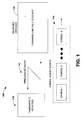
- FIG. 1 is a conceptual block diagram illustrating an example of a wireless network system for forward link only networks (FLOs).
- FLOs forward link only networks
- FIG. 2 is a conceptual block diagram illustrating an example of a receiver device that may be employed in a wireless communication environment.
- FIG. 3 is a conceptual block diagram illustrating an example of a system that includes a transmitter device and one or more receiver devices.
- FIG. 4 illustrates an exemplary FLO physical layer superframe.
- FIG. 5 illustrates an exemplary interlace structure
- FIG. 6 is an exemplary table for slot-to-interlace mapping.
- FIG. 7 is a conceptual block diagram illustrating an exemplary hardware implementation architecture for generalized slot-to-interlace maps.
- FIG. 8 is a conceptual block diagram illustrating an example of the functionality of a processing system in a transmitter or receiver device.
- FIG. 9 is a flow chart illustrating an exemplary operation of providing slot interlaces or providing communication at a transmitter or receiver device.
- FIG. 1 is a conceptual block diagram illustrating an example of a wireless network system 100 for forward link only networks.
- the system 100 includes one or more transmitter devices 110 that can communicate across a wireless network 112 to one or more receiver devices 120.
- a receiver device 120 can be any suitable communications device such as a cell phone, a wireless phone, a wired phone, a laptop computer, a desktop computer, a personal digital assistant (PDA), a data transceiver, a modem, a pager, a camera, a game console, an MPEG Audio Layer-3 (MP3) player, a media gateway system, an audio communications device, a video communications device, a multimedia communications device, a component of any of the foregoing devices (e.g., a printed circuit board(s), an integrated circuit(s), or a circuit component(s)), or any other suitable audio, video, or multimedia device, or a combination thereof.
- PDA personal digital assistant
- MP3 MPEG Audio Layer-3
- a transmitter device 110 may be any suitable communications device that can transmit, such as a base station or a broadcasting station.
- any of the devices described above in this paragraph can be a receiver device, if it can receive a signal, or a transmitter device, if it can transmit a signal.
- any of the receiver devices described above can be a transmitter device, if it can transmit a signal
- any of the transmitter devices described above can be a receiver device, if it can receive a signal.
- a device can be referred to as a user device when it is used, or to be used, by a user.
- Portions of the receiver devices 120 may be employed to decode a symbol subset 130 and other data such as multimedia data.
- the symbol subset 130 may be transmitted in an Orthogonal Frequency Division Multiplexing (OFDM) network that employs forward link only (FLO) protocols for multimedia data transfer.
- OFDM Orthogonal Frequency Division Multiplexing
- FLO forward link only
- Channel estimation can be based on uniformly spaced pilot tones inserted in the frequency domain, and in respective OFDM symbols.
- FIG. 2 is a conceptual block diagram illustrating an example of a receiver device 200 that may be employed in a wireless communication environment, in accordance with one or more aspects set forth herein.
- a receiver device 200 may include a receiver 202 that receives a signal from, for instance, a receive antenna (not shown), and performs typical actions (e.g., filters, amplifies, down converts, etc.) on the received signal and digitizes the conditioned signal to obtain samples.
- a demodulator 204 can demodulate and provide received pilot symbols to a processing system 206 for channel estimation.
- a FLO channel component 210 may be provided to process FLO signals. This can include, for instance, digital stream processing and/or positioning location calculations among other processes.
- a processing system 206 may be, for example, a processor dedicated to analyzing information received by the receiver 202 and/or generating information for transmission by a transmitter 216, a processor that controls one or more components of the receiver device 200, or a processor that analyzes information received by the receiver 202, generates information for transmission by the transmitter 216, and controls one or more components of the receiver device 200.
- the processing system 206 may be implemented using software, hardware, or a combination of both.
- Software shall be construed broadly to mean instructions, data, or any combination thereof, whether referred to as software, firmware, middleware, microcode, hardware description language, or otherwise.
- the processing system 206 may be implemented with one or more processors.
- a processor may be a general-purpose microprocessor, a microcontroller, a Digital Signal Processor (DSP), an Application Specific Integrated Circuit (ASIC), a Field Programmable Gate Array (FPGA), a Programmable Logic Device (PLD), a controller, a state machine, gated logic, discrete hardware components, or any other suitable entity that can perform calculations or other manipulations of information.
- DSP Digital Signal Processor
- ASIC Application Specific Integrated Circuit
- FPGA Field Programmable Gate Array
- PLD Programmable Logic Device
- the receiver device 200 can additionally include a memory 208 that is operatively coupled to the processing system 206 and that can store information related to data processing.
- Readable media may include storage integrated into a processor, such as might be the case with an ASIC, and/or storage external to a processor such as the memory 208.
- readable media may include one or more of volatile memory, nonvolatile memory, a Random Access Memory (RAM), a flash memory, a Read Only Memory (ROM), a Programmable Read-Only Memory (PROM), an Erasable PROM (EPROM), a register, a hard disk, a removable disk, a CD-ROM, a DVD, or any other suitable storage device.
- readable media may include a transmission line or a carrier wave that encodes a data signal.
- a readable medium may be a computer-readable medium encoded or stored with a computer program or instructions. The computer program or instructions may be executable by a transmitter or receiver device or by a processing system of a transmitter or receiver device.
- the receiver device 200 may further include a background monitor 214 for processing FLO data, a symbol modulator 214, and the transmitter 216 that transmits the modulated signal.
- FIG. 3 is a conceptual block diagram illustrating an example of a system 300 that includes a transmitter device 302 and one or more receiver devices 304.
- the transmitter device 302 may include a receiver 310 that receives signal(s) from the one or more receiver devices 304 through one or more receive antennas 306, and a transmitter 322 that transmits to the one or more receiver devices 304 through one or more transmit antennas 308.
- the receiver 310 can be operatively associated with a demodulator 312 that demodulates received information. Demodulated symbols can be analyzed by a processing system 314 that is similar to the processing system 206 described above, which may be coupled to a memory 316 that stores information related to data processing.
- the processing system 314 may be further coupled to a FLO channel component 318 that facilitates processing of FLO information associated with one or more respective receiver devices 304.
- the FLO channel component 318 can append information to a signal related to an updated data stream for a given transmission stream for communication with the receiver devices 304, to provide an indication that a new optimum channel has been identified and acknowledged.
- a modulator 320 may also be provided to multiplex a signal for transmission by the transmitter 322.
- FIG. 4 illustrates an exemplary FLO physical layer superframe 400.
- a superframe 400 may include, among others, Time Division Multiplexed (TDM) pilots (e.g., TDM Pilot 1 and TDM Pilot 2), Wide-Area Identification Channel (WIC), Local-Area Identification Channel (LIC), Overhead Information Symbols (OIS), four frames of data (e.g., Frame 1 through Frame 4), Positioning Pilot Channel (PPC), and Signaling Parameter Channel (SPC).
- TDM pilots may allow rapid acquisition of the OIS.
- the OIS may describe the location of the data for each media service in the superframe.
- a superframe structure is not limited to what is illustrated in FIG. 4 , and a superframe may consist of less elements or more elements than what is illustrated in FIG. 4 .
- OFDM is a form of multi-carrier modulation.
- the available bandwidth may be divided into N bins, referred to as subcarriers, with each subcarrier modulated, for example, by a quadrature amplitude modulated (QAM) symbol.
- QAM quadrature amplitude modulated
- transmission and reception may be based on using 4096 (4K) subcarriers, and the QAM modulation symbols may be chosen, for example, from a QPSK or 16-QAM alphabet.
- Each superframe may include multiple OFDM symbols.
- a superframe may include 200 OFDM symbols per MHz of available bandwidth (e.g., 1200 OFDM symbols for 6 MHz).
- an exemplary interlace structure may include, for example, 8 interlaces.
- the interlace indices range from 0 to 7 (i.e., 10, I1, I2, I3, I4, I5, I6, I7 and I8).
- Each interlace may consist of, for example, 500 subcarriers that are evenly spaced across the signal bandwidth. Between the adjacent subcarriers within each interlace, there are 7 subcarriers, each of which belongs to a different interlace. In each OFDM symbol, one interlace may be assigned to the pilot interlace and may be used for channel estimation. Hence, 500 subcarriers may be modulated with known (pilot) modulation symbols.
- FIG. 5 illustrates an exemplary interlace structure/function
- an interlace structure/function is not limited to this configuration, and it can be of other type of configurations (e.g., having any number of interlaces).
- Each interlace may be uniformly distributed in frequency, so that it may achieve the full frequency diversity within the available bandwidth.
- These interlaces may be assigned to logical channels that vary in terms of duration and number of actual interlaces used. This provides flexibility in the time diversity achieved by any given data source. Lower data rate channels can be assigned fewer interlaces to improve time diversity, while higher data rate channels may utilize more interlaces to minimize the radio's on-time and reduce power consumption.
- FIG. 6 is an exemplary table for slot-to-interlace mapping.
- the vertical axis indicates slot indices.
- the horizontal axis indicates symbol indices.
- the values in the table indicate interlace indices.
- a slot may refer to a group of symbols
- an interlace may refer to a group of subcarriers
- each slot may be mapped to an interlace in each symbol period based on a slot-to-interlace mapping scheme.
- a slot which may be referred to as a transmission slot, may correspond to an interlace or a group of modulation symbols in one symbol period.
- a slot may be mapped to one or more interlaces, and an interlace may be mapped to one or more slots.
- a time unit for a frame may include a MAC time unit at the MAC (or allocation) layer and an OFDM symbol period at the physical (PHY) layer.
- a symbol period can refer to a MAC time unit in the context of physical layer channel (PLC) allocation or an OFDM symbol period in the context of subcarrier allocation.
- a symbol period may refer to a time unit of a symbol index.
- the subject technology is not limited to this number of subcarriers or FFT size.
- the subject technology is capable of multiplexing and transmitting multiple data streams in OFDM systems of various FFT sizes. For an OFDM system with a 4K FFT size, a group of 500 modulation symbols, forming a slot, may be mapped into one interlace.
- a slot may be fixed across different FFT sizes.
- the size of an interlace may be 1/8 th the number of active subcarriers, and a slot may be mapped into either a fractional or a multiple (including one) interlaces based on the FFT size.
- the interlace(s) assigned to a slot may reside in multiple OFDM symbol periods. For example, for a 2K FFT size, a slot (i.e., 500 modulation symbols) maps into 2 interlaces over 2 consecutive 2K OFDM symbols. Similarly, for a 1K FFT size, a slot maps into 4 interlaces over 4 consecutive 1K OFDM symbols.
- the number of useable subcarriers for 1K, 2K, 4K and 8K FFT sizes, respectively, may be 1000, 2000, 4000 and 8000, since the useable subcarriers may not include, for example, guard subcarriers. That is, an FFT size of 1K contains 1024 subcarriers, where 24 of the subcarriers may be used as guard subcarriers, for example.
- the number of guard subcarriers may, for example, increase proportionally with FFT size.
- a slot maps into half of an interlace over half of an 8K OFDM symbol.
- a MAC time unit may comprise, for example, 8 slots.
- Table 1 shows exemplary relationships between FFT sizes of 1K, 2K, 4K and 8K and their respective number of OFDM symbols per MAC time unit, number of subcarriers per interlace, and number of interlaces per slot: Table 1 FFT Size Number of OFDM Symbols per MAC Time Unit Number of Subcarriers per Interlace Number of Interlaces per Slot 1024 (1K) 4 125 4 2048 (2K) 2 250 2 4096 (4K) 1 500 1 8192 (8K) 1 ⁇ 2 1000 1 ⁇ 2
- the subject technology is capable of MAC layer multiplexing over MAC time units and slots, regardless of the FFT size of the OFDM system.
- the physical layer can map MAC time units and slots to OFDM symbols and interlaces, respectively, for various FFT sizes.
- a system may include multiple slots per symbol (e.g., 8 slots per symbol as shown in FIG. 6 ). While one slot (e.g., slot 0) may be assigned to pilot symbols, the other slots (e.g., slots 1 through 7) may be made available for allocation to data symbols. Pilot symbols are known a priori by the transmitter and receiver devices. Pilot symbols may be used by a transmitter or receiver device for, by way of illustration, frame synchronization, frequency acquisition, timing acquisition, and/or channel estimation. In this example, slot 0 may be referred to as a pilot slot, and slots 1 through 7 may be referred to as data slots. Alternatively, multiple slots (e.g., slot 1 and 3) may be assigned to pilot symbols, and the remaining slots may be allocated to data symbols.
- multiple slots e.g., slot 1 and 3
- slots 1 and 3 may be referred to as pilot slots, and the remaining slots may be referred to as data slots.
- FIG. 6 illustrates an exemplary slot structure/function, a slot structure/function is not limited to this configuration.
- a slot structure/function can be of other type of configurations (e.g., a slot structure may have any number of slots, and the slots may be allocated in many different ways and for various types of information).
- each of the slots is assigned or mapped to an interlace.
- slot 1 is assigned to interlaces 3, 1, 0, 7, 5, 4, etc. over the successive OFDM symbol indices 4, 5, 6, 6, 7, 8, 0, etc.
- a slot interlace may refer to an interlace to which a slot is mapped or to be mapped.
- a pilot interlace may refer to a slot interlace associated with a pilot slot.
- a slot interlace may refer to a slot to which an interlace is mapped or to be mapped.
- a pilot interlace may refer to a slot interlace associated with a pilot interlace.
- a slot interlace may refer to a slot-to-interlace map function or an interlace-to-slot map function.
- a slot-to-interlace map function and an interlace-to-slot map function may be the same or equivalent, except that a slot-to-interlace map function may utilize a slot (or a slot index) as an input and provide an interlace (or an interlace index) as an output and that an interlace-to-slot map function may utilize an interlace (or an interlace index) as an input and provide a slot (or a slot index) as an output.
- a slot such as a slot, an interlace, a pilot slot, a pilot interlace, a symbol, and the like are sometimes used to refer to a slot index, an interlace index, a pilot slot index, a pilot interlace index, and a symbol index, respectively.
- a FLO system is capable of multicasting various services, such as live video and audio streams (e.g., News, Music or Sports channels).
- a service can be viewed as an aggregation of one or more related data components, such as the video, audio, text or signaling associated with a service.
- Each FLO service may be carried over one or more logical channels, referred to as Multicast Logical Channels (MLCs).
- MLCs Multicast Logical Channels
- the video and audio components of a given service may be sent on multiple MLCs (e.g., two different MLCs).
- One or more slots for data symbols may be used for MLCs.
- slots 1-3 may be used for video components of a given service
- slots 4-7 may be used for audio components of a given service.
- Exemplary systems and methods for a generalized slot-to-interlace map for FLO are described in detail below. Such systems and methods can support a whole family of slot-to-interlace maps in FLO transmitter and receiver devices.
- Generalized slot-to-interlace maps can provide different length channel estimates that can be computed at a receiver device as well as better Doppler resilience.
- Generalized slot-to-interlace maps are sometimes referred to as flexible slot-to-interlace maps.
- a particular slot-to-interlace map may sometimes be referred to by the corresponding pilot staggering pattern used in the slot-to-interlace map.
- the FLO air interface specification for 4K mode (TIA-1099) along with its associated implementation can support a staggering pattern referred to as the (2,6) pattern.
- the pilot interlace alternates between interlaces 2 and 6 across successive OFDM symbols in a superframe.
- a (2,6) staggering pattern provides pilot observations from two distinct interlaces 2 and 6. This allows computation of channel estimation up to a length of 1024 in 4K mode operation. While 1024 length channel estimates may suffice for deployments in regions such as the United States, support for longer channel estimates (longer than two pilot interlaces) may be required in other modes of FLO deployment (e.g., 2K mode or VHF band deployment).
- Slot-to-interlace map patterns such as those using (0,3,6) and (0,2,4,6) pilot staggering patterns may also be utilized to allow flexibility in channel estimation. These patterns can provide a maximum of 4096 and 2048 length channel estimates, respectively, according to one exemplary implementation. It is also possible to estimate longer channel delay spread (e.g., greater than 4096 and greater than 2048) with higher channel estimation error.
- flexible slot-to-interlace maps may be utilized for OIS and data symbols.
- TDM pilot such as TDM Pilot 1 and TDM Pilot 2
- WIC such as TDM Pilot 1 and TDM Pilot 2
- WIC such as TDM Pilot 1
- LIC such as TDM Pilot 2
- PPC PPC
- SPC symbols may have fixed interlaces independent of the slot-to-interlace map in use for the rest of the superframe.
- a FLO receiver device may determine the slot-to-interlace map to be used after decoding the SPC symbols, which occur at the end of the superframe.
- Exemplary implementations of generalized slot-to-interlace maps using the (0,3,6), (0,2,4,6) and (2,6) pilot staggering patterns are described in detail below.
- the slot-to-interlace maps as well as the associated implementations are based on the concept of pilot interlaces and distance vectors for different data slots.
- the length of a distance vector may be the number of interlaces minus the number of pilot interlaces.
- 8 interlaces and 8 slots are used.
- the subject technology is not limited to these numbers, and any number of interlaces and any number of slots may be utilized.
- a pilot interlace vector ( I 0 ) may be determined by the staggering pattern.
- One or more distance vectors ( D ) may be defined for each slot-to-interlace map. The distance vectors can be used to determine the interlace index for each data slot.
- data slots may be arranged using the remaining interlaces such that the relative distance of the resulting interlace for a given slot can be obtained from the rotations of the one or more distance vectors. An exemplary implementation of this is described below.
- the pilot jump is 3, and I 0 is determined as follows: (i) start with 0 from the staggering pattern, (ii) add the pilot jump of 3 to the initial value 0 to obtain 3 as the next value, (iii) add 3 to obtain 6, (iv) add 3 to obtain 9, which is translated to 1, (v) add 3 to obtain 12, which is translated to 4, (vi) add 3 to obtain 15, which is translated to 7, (vii) add 3 to obtain 18, which is translated to 2, and (viii) add 3 to obtain 21, which is translated to 5.
- the translation described above may be performed using, for example, the total number of interlaces and a modulo operation.
- n denote the OFDM symbol index in the superframe, where n goes from 0 through 1199.
- symbol index 0 corresponds to TDM1.
- s denote the slot index so that s ranges from 0 through 7.
- slot interlace I [ s,n ] correspond to the interlace to which the slot s is mapped in OFDM symbol index n .
- s in I [ s , n ] may take values from 0 through 7.
- slot interlace I [0, n ] may be referred to as a pilot interlace.
- the resulting map ensures that in a block of 7 successive OFDM symbols, every slot occurs at all the possible distances from the pilot interlace. Furthermore, in a block of 56 successive OFDM symbols, each slot occupies every available interlace exactly 7 times. Each slot goes through all the available interlaces at least once in a window of 17 OFDM symbols. It is also guaranteed that there are at least three intermediate OFDM symbols before a particular interlace is assigned to the same slot.
- An exemplary generalized slot-to-interlace map based on the (2,6) staggering pattern can be realized using the pilot interlace and distance vectors.
- one pilot interlace vector ( I 0 ) and two different distance vectors ( D o and D 1 ) are used to realize the entire slot-to-interlace pattern.
- slot interlace I [ s , n ] which is the interlace corresponding to slot s in OFDM symbol index n .
- An exemplary generalized slot-to-interlace map based on the (0,2,4,6) staggering pattern can be realized using a pilot interlace and a distance vector.
- a pilot interlace vector ( I 0 ) and a distance vector ( D ) are used to realize the entire slot-to-interlace pattern.
- slot interlace I [ s,n ] can be determined as follows:
- each slot (except for a pilot slot) is assigned to every interlace at least once in every 10 successive OFDM symbols.
- An interlace is repeated for a slot only after three OFDM symbols.
- every slot occupies all the possible distances from the pilot interlace in a block of 7 successive OFDM symbols.
- each slot occupies interlaces 0, 2, 4 and 6 three times and interlaces 1, 3, 5 and 7 four times.
- each of slots 1 through 7 is assigned to each of interlaces 0, 1, 2, 3, 4, 5, 6, and 7 at least once in every 10 successive OFDM symbols.
- slot 1 is assigned to interlace 3 for OFDM symbol index 4
- is assigned to interlace 2 for OFDM symbol index 10 is assigned to interlace 1 for OFDM symbol index 11
- is assigned to interlace 7 for OFDM symbol index 12 is assigned to interlace 6 for OFDM symbol index 13.
- an interlace index is repeated for a slot only after 3 symbols.
- interlace 0 is repeated only after 3 successive OFDM symbols indices. This is the same for interlace 2, interlace 4 and interlace 6.
- FIG. 6 illustrates that every slot occupies all the possible distances from the pilot interlace in 7 successive OFDM symbols.
- slot 0 is for the pilot interlace, and is assigned to interlaces 0, 2, 4, 6, 0, 2, and 4 for OFDM symbol indices 4, 5, 6, 7, 8, 9, and 10, respectively.
- Slot 3 is assigned to interlaces 6, 5, 3, 2, 1, 7, and 6 for OFDM symbol indices 4, 5, 6, 7, 8, 9, and 10, respectively.
- the distance between slot 3 and slot 0 is the absolute value of the difference between the interlace indices of slot 3 and slot 0.
- the distance is 6, 3, 7 (which is a translation of -1), 4 (which is a translation of -4), 1, 5, and 2 for OFDM symbol indices 4, 5, 6, 7, 8, 9, and 10, respectively.
- the absolute value can be obtained, for example, by performing a modulo operation.
- one or more pilot interlace vectors may be utilized, and one or more distance vectors (e.g., D 0 , D 1 , D 2 , etc.) may be utilized.
- the number of slots and the number of interlaces are not limited to 8, and each of them may be any number. Thus, there may be p number of slots, and q number of interlaces. The variables p and q may be the same.
- the length of each of the pilot interlace vectors may be q .
- one or more (or all) of the following properties may be associated with generalized slot-to-interlace mapping:
- FIG. 7 is a conceptual block diagram illustrating exemplary hardware implementation architecture for generalized slot-to-interlace maps.
- a processing system 710 of a transmitter or receiver device may include a pilot interlace vector unit 710, a distance vector unit 730, and a slot interlace computation unit 740.
- 8 slots and 8 interlaces are used, but the subject technology is not limited to these numbers of slots and interlaces.
- Various parameters required for computing the slot-to-interlace map such as the pilot interlace vector, distance vectors and other control parameters like shift_enable may be programmed by the software to allow easy programmability in the mapping used.
- the software may be able to directly program the hardware registers (e.g., the pilot interlace vector unit 710 and the distance vector unit 730) that contain some of these parameters. These parameters may be programmed at power up (based on default parameters) or after processing the SPC symbols.
- the hardware is awake when the software attempts to program these registers. Since the hardware sleep timeline is available in software, the software can readily handle sleep-related issues.
- Providing the direct control to software may ensure that OIS decoding is enabled at the appropriate time in software. OIS decoding may be enabled after the slot-to-interlace parameters are programmed in the hardware.
- the pilot interlace vector unit 710 may include a pilot interlace vector I o that includes, for example, an 8 x 1 vector programmed by the software. Each element of the vector may be 3 bits long (to represent one of eight interlaces from 000 to 111). For staggering patterns such as (2,6), the pattern may be repeated periodically until all eight elements in the vector are used up. For example, a (2,6) staggering pattern may generate a pilot interlace vector I o of (2,6,2,6,2,6,2,6). A (0,3,6) staggering pattern may generate a pilot interlace vector I o of (0,3,6,1,4,7,2,5). A (0,2,4,6) staggering pattern may generate a pilot interlace vector I o of (0,2,4,6,0,2,4,6).
- the distance vector unit 730 which includes, for example, an 8 x 7 distance vector table.
- Each entry in this table may be represented using three bits.
- the table may include 8 rows, each of length 21 bits.
- Each row of this table corresponds to one distance vector.
- pilot interlace vector if the number of distance vectors is less than 8, then the distance vectors are repeated periodically to fill up the entire table. Therefore, in the case of (0,3,6) pattern, one vector is repeated 8 times to fill up the table.
- (2,6) staggering pattern where there are two distinct distance vectors, each distance vector occurs four times in alternate locations in the table. Software can handle the periodic repetitions while writing to the tables.
- a shift_enable flag 775 (1 bit) can be used by the hardware to enable or disable the cyclic rotation of the distance vector based on the OFDM symbol index.
- the shift_enable flag 775 may be also initialized by the software while initializing the pilot interlace vector and the distance vectors.
- OFDM symbol index n in the following description corresponds to the OFDM symbol index in the superframe.
- Hardware first uses the OFDM symbol index n for which the slot-to-interlace map is to be generated, selects the three least significant bits (LSBs) (modulo 8 operation), and uses the three LSBs to index into the pilot interlace vector to obtain the pilot interlace.
- the pilot interlace may be given by the three bits in the vector which occupy the positions (n mod 8) * 3, (n mod 8) * 3 + 1 and (n mod 8) * 3 + 2. Let this be denoted by I [0, n ].
- the OFDM symbol index n may also be used to index into the distance vector as well as the rotation factor that is used on the distance vector.
- the shift_enable flag 775 which is set by the software (depending on the slot-to-interlace map being used), can determine if a non-zero rotation is to be used on the distance vector. If the shift_enable flag 775 is set, then the OFDM symbol index n is first shifted to the left by 1 using a left shift unit 795 (multiplication by 2), and then a modulo 7 operation is performed on the result using a modulo 7 unit 790.
- a multiplier 770 multiplies the result by 3 (to account for 3 bits used by each entry in the distance vector table) to arrive at R n , which is used as an argument for a right cyclic shift unit 742.
- the OFDM symbol index n may also be used to select the appropriate distance vector row in the distance vector matrix.
- the three LSBs of the OFDM symbol index e.g., n mod 8
- the distance vector D is then cyclically shifted to the right by the argument given by R n to arrive at D R n .
- the software can perform a cyclic extension of the 24 bit vector to 32 bits by placing the 8 LSBs at the front.
- Such an extended vector can help in the cyclic shift operation for the hardware.
- D R n corresponds to the 24 LSBs of the cyclically shifted vector.
- the slot interlaces 725 for data slots 1 through 7 in the OFDM symbol index n can be obtained as follows.
- the pilot interlace I [0, n ] that was obtained previously can be added to the three LSBs of D R n using an adder 745.
- a modulo 8 operation can be performed on the result using a modulo 8 unit 750.
- the result may be placed into a data interlace table unit 760, which may include a 1 x 7 vector. Each element of the vector may be 3 bits long.
- the first result may be a slot interlace corresponding to slot 1.
- the interlace index is given by the operation ( I [0, n ]+ D R n (3 s -3:3 s -1))mod8. Note that in D R n , ( x : y ) corresponds to bit locations x, x-1,..., y in the above expression.
- the interlace indices obtained for all the seven data slots and the pilot slot may be stored in a look up table (not shown) that can then be indexed using the slot index.
- a processing system 710 shown in FIG. 7 may be also utilized to map an interlace to a slot when OFDM symbols are received.
- the pilot interlace 720 may provide a pilot slot(s) for a given pilot interlace(s)
- the slot interlaces 725 may provide a slot(s) for a given interlace(s).
- the processing system 710 may be preprogrammed with one or more pilot interlace vectors, one or more distance vectors and optionally one or more rotation factors. Alternatively, the processing system 710 may receive some or all of these via other suitable means (e.g., a FLO network, other type of network, other type of communication).
- the processing system 710 may provide the corresponding slot(s) using a slot interlace computation unit. Also, for a give symbol index and a pilot interlace(s), the processing system 710 may provide the corresponding pilot slot(s) using the slot interlace computation unit.
- the implementation of the slot interlace computation unit may be similar to or different than the implementation of the slot interlace computation unit 740.
- a modulo 7 operation that may be used in a slot-to-interlace map implementation is explained in detail below.
- a 2 n mod 7 operation may be performed where n is the OFDM symbol index in the superframe.
- a modulo 7 operation is performed using adders only. A basic concept is described below.
- any power of 8 is also congruent to 1 modulo 7.
- Each p i represents three consecutive bits at the location (3 i + 2 : 3 i ) in the binary representation of k . Therefore, successive three bits in the form of (3i + 2 : 3 i ) can be added up until the final result is reduced to 3 bits.
- this technique can be applied to the OFDM symbol index n in the superframe as follows. Note that when the OFDM symbol index n is a 11 bit number in a FLO system across all bandwidths, 2 n is a 12 bit number.
- This implementation uses 6 adders. It is also possible to use a higher power of 8 (e.g., 64) and reduce the operations to 2 additions. A look up table may be used to map it back to the final result modulo 7.
- a modulo 7 operation may be performed in the following manner.
- the receiver 202 of the receiver device 200 may receive a signal.
- the demodulator 204 may perform demodulation on the received signal and provide OFDM symbols to the processing system 206, which may separate the OFDM symbols into interlaces and map the interlaces into slots using one or more pilot interlaces and one or more slot interlaces.
- the processing system 206 may further generate modulation symbols from the slots and convert the modulation symbols to data streams.
- the transmitter device 302 may receive data streams and convert the data streams to symbols.
- the processing system 314 of the transmitter device 302 may assign the symbols into slots and map the slots into interlaces using one or more pilot interlaces and one or more slot interlaces.
- the modulator 320 may perform modulation to generate a modulated signal, and the transmitter 322 may transmit the modulated signal.
- FIG. 8 is a conceptual block diagram illustrating an example of the functionality of a processing system in a transmitter or receiver device.
- a processing system 314 or 206 of a transmitter or receiver device 302 or 200 includes a module 810 for including one or more pilot interlace vectors and a module 820 for including one or more distance vectors.
- the processing system 206 or 314 also includes a module 830 for providing a first slot interlace based on the one or more pilot interlace vectors and a module 840 for providing a second slot interlace based on the first slot interlace and the one or more distance vectors.
- FIG. 9 is a flow chart illustrating an exemplary operation of providing slot interlaces or providing communication at a transmitter or receiver device.
- a processing system 314 or 206 of a transmitter or receiver device 302 or 200 may receive one or more pilot interlace vectors.
- the processing system 314 or 206 may receive one or more distance vectors.
- it may provide a first slot interlace based on the one or more pilot interlace vectors.
- the processing system 314 or 206 may provide a second slot interlace based on the first slot interlace and the one or more distance vectors.
- a readable medium may be encoded or stored with instructions executable by a transmitter or receiver device, or by a processing system of such a device, where the instructions include code for the steps 910, 920, 930 and 940 described above.
- hardware architecture can be used to implement a family of slot-to-interlace maps through the configuration of some hardware registers.
- the architecture can support slot-to-interlace maps with different pilot staggering patterns. Channel estimation ability and Doppler resilience depend on the pilot staggering pattern in an OFDM system such as FLO.
- FLO OFDM system
- a single FLO receiver device can support different slot-to-interlace maps that may be deployed in different networks.
- the architecture also supports backward compatibility with the FLO air interface specification.
- the pilot observations obtained from multiple OFDM symbols may correspond to as many distinct subcarriers as possible to ensure a channel estimate that satisfies the delay spread requirements of the communication system.
- the data symbols may be interspersed among both the pilot subcarriers as well as the total available set of subcarriers in the OFDM system so that the data symbols may enjoy the benefits of channel estimation as well as frequency diversity. Therefore, slot-to-interlace maps play a vital role in OFDM systems.
- the hardware and software implementations presented above are exemplary implementations.
- the subject technology is not limited to these implementations, and other suitable implementations may be used.
- the subject technology is also not limited to a FLO system, and it may be used in a variety of communications systems. While staggering patterns (2,6), (0,3,6) and (0,2,4,6) are described above, these are merely examples, and the subject technology is not limited to these examples.
- the descriptions related to OFDM symbols and OFDM symbol index may be applicable to other symbols and symbol index.
- symbol used herein may refer to an OFDM symbol, any other type of symbol, data, or information.
- vector used herein may refer to an array, a group, a set, or a plurality of items.
- the term “map” used herein may refer to assign or allocate, and vice versa.
- a component may be, but is not limited to being, a process running on a processor, an object, an executable, a thread of execution, a program, and/or a computer.
- an application running on a communications device and the device can be a component.
- One or more components may reside within a process and/or thread of execution, and a component may be localized on one computer and/or distributed between two or more computers.
- these components can execute from various readable media having various data structures stored thereon.
- the components may communicate over local and/or remote processes such as in accordance with a signal having one or more data packets (e.g., data from one component interacting with another component in a local system, distributed system, and/or across a wired or wireless network such as the Internet).
- a signal having one or more data packets (e.g., data from one component interacting with another component in a local system, distributed system, and/or across a wired or wireless network such as the Internet).
Landscapes
- Engineering & Computer Science (AREA)
- Signal Processing (AREA)
- Computer Networks & Wireless Communication (AREA)
- Mobile Radio Communication Systems (AREA)
- Two-Way Televisions, Distribution Of Moving Picture Or The Like (AREA)
- Error Detection And Correction (AREA)
- Detection And Prevention Of Errors In Transmission (AREA)
Applications Claiming Priority (3)
| Application Number | Priority Date | Filing Date | Title |
|---|---|---|---|
| US95195007P | 2007-07-26 | 2007-07-26 | |
| US95195107P | 2007-07-26 | 2007-07-26 | |
| US11/834,671 US8477809B2 (en) | 2003-09-02 | 2007-08-06 | Systems and methods for generalized slot-to-interlace mapping |
Publications (2)
| Publication Number | Publication Date |
|---|---|
| EP2028785A2 true EP2028785A2 (fr) | 2009-02-25 |
| EP2028785A3 EP2028785A3 (fr) | 2009-06-24 |
Family
ID=40210819
Family Applications (1)
| Application Number | Title | Priority Date | Filing Date |
|---|---|---|---|
| EP08006309A Ceased EP2028785A3 (fr) | 2007-07-26 | 2008-03-31 | Systèmes et procédés pour mappage généralisé de créneaux temporels sur des entrelacements |
Country Status (4)
| Country | Link |
|---|---|
| EP (1) | EP2028785A3 (fr) |
| AU (1) | AU2008278607A1 (fr) |
| RU (1) | RU2010107061A (fr) |
| WO (1) | WO2009015399A2 (fr) |
Cited By (1)
| Publication number | Priority date | Publication date | Assignee | Title |
|---|---|---|---|---|
| CN102668435A (zh) * | 2009-11-17 | 2012-09-12 | 索尼公司 | 在提供递增冗余的广播系统中广播数据的发送机和发送方法 |
Families Citing this family (2)
| Publication number | Priority date | Publication date | Assignee | Title |
|---|---|---|---|---|
| EA039221B1 (ru) * | 2018-11-07 | 2021-12-20 | Открытое акционерное общество "Межгосударственная Корпорация Развития" | Приемник |
| CN117972317B (zh) * | 2024-03-29 | 2024-06-14 | 中国民用航空飞行学院 | 一种面向飞行员胜任能力的韧性画像方法 |
Citations (7)
| Publication number | Priority date | Publication date | Assignee | Title |
|---|---|---|---|---|
| US20050058089A1 (en) | 2003-09-02 | 2005-03-17 | Rajiv Vijayan | Multiplexing and transmission of multiple data streams in a wireless multi-carrier communication system |
| US20050135308A1 (en) | 2003-10-24 | 2005-06-23 | Qualcomm Incorporated | Frequency division multiplexing of multiple data streams in a wireless multi-carrier communication system |
| WO2005112378A1 (fr) | 2004-05-04 | 2005-11-24 | Qualcomm Incorporated | Transmission de pilotes decales pour l'estimation d'un canal et le suivi temporel |
| WO2005114940A1 (fr) * | 2004-05-18 | 2005-12-01 | Qualcomm Incorporated | Convertisseurs fentes-entrelacements et entrelacements-fentes pour systeme ofdm |
| WO2006086878A1 (fr) | 2005-02-15 | 2006-08-24 | Nortel Networks Limited | Systeme d'acces radio et procede d'utilisation ofdm et cdma pour une emission de donnees large bande |
| WO2006099222A1 (fr) | 2005-03-10 | 2006-09-21 | Qualcomm Incorporated | Synchronisation de temporisation et estimation de voie au niveau d'une transition entre des formes d'onde de zone locale et de zone etendue au moyen d'un pilote mrt designe |
| US20060222108A1 (en) | 2005-03-10 | 2006-10-05 | Cousineau Kevin S | Determining modulo count in sleep capable system |
-
2008
- 2008-03-31 EP EP08006309A patent/EP2028785A3/fr not_active Ceased
- 2008-08-06 WO PCT/US2008/072372 patent/WO2009015399A2/fr not_active Ceased
- 2008-08-06 RU RU2010107061/07A patent/RU2010107061A/ru unknown
- 2008-08-06 AU AU2008278607A patent/AU2008278607A1/en not_active Abandoned
Patent Citations (7)
| Publication number | Priority date | Publication date | Assignee | Title |
|---|---|---|---|---|
| US20050058089A1 (en) | 2003-09-02 | 2005-03-17 | Rajiv Vijayan | Multiplexing and transmission of multiple data streams in a wireless multi-carrier communication system |
| US20050135308A1 (en) | 2003-10-24 | 2005-06-23 | Qualcomm Incorporated | Frequency division multiplexing of multiple data streams in a wireless multi-carrier communication system |
| WO2005112378A1 (fr) | 2004-05-04 | 2005-11-24 | Qualcomm Incorporated | Transmission de pilotes decales pour l'estimation d'un canal et le suivi temporel |
| WO2005114940A1 (fr) * | 2004-05-18 | 2005-12-01 | Qualcomm Incorporated | Convertisseurs fentes-entrelacements et entrelacements-fentes pour systeme ofdm |
| WO2006086878A1 (fr) | 2005-02-15 | 2006-08-24 | Nortel Networks Limited | Systeme d'acces radio et procede d'utilisation ofdm et cdma pour une emission de donnees large bande |
| WO2006099222A1 (fr) | 2005-03-10 | 2006-09-21 | Qualcomm Incorporated | Synchronisation de temporisation et estimation de voie au niveau d'une transition entre des formes d'onde de zone locale et de zone etendue au moyen d'un pilote mrt designe |
| US20060222108A1 (en) | 2005-03-10 | 2006-10-05 | Cousineau Kevin S | Determining modulo count in sleep capable system |
Non-Patent Citations (1)
| Title |
|---|
| U. SPARMANN ET AL.: "On the effectiveness of Residue Code Checking for Parallel Two's Complement Multipliers", IEEE TRANSACTIONS ON VERY LARGE SCALE INTEGRATION (VLSI) SYSTEMS, vol. 4, no. 2, June 1996 (1996-06-01) |
Cited By (4)
| Publication number | Priority date | Publication date | Assignee | Title |
|---|---|---|---|---|
| CN102668435A (zh) * | 2009-11-17 | 2012-09-12 | 索尼公司 | 在提供递增冗余的广播系统中广播数据的发送机和发送方法 |
| CN102668435B (zh) * | 2009-11-17 | 2015-09-16 | 索尼公司 | 在提供递增冗余的广播系统中广播数据的发送机和接收机 |
| US9444582B2 (en) | 2009-11-17 | 2016-09-13 | Sony Corporation | Transmitter and receiver for broadcasting data and providing incremental redundancy |
| US10250358B2 (en) | 2009-11-17 | 2019-04-02 | Saturn Licensing Llc | Transmitter and receiver for transmitting basic codeword portion and auxiliary codeword portion of a codeword in different frames |
Also Published As
| Publication number | Publication date |
|---|---|
| WO2009015399A3 (fr) | 2009-07-02 |
| EP2028785A3 (fr) | 2009-06-24 |
| AU2008278607A1 (en) | 2009-01-29 |
| WO2009015399A2 (fr) | 2009-01-29 |
| RU2010107061A (ru) | 2011-09-10 |
Similar Documents
| Publication | Publication Date | Title |
|---|---|---|
| US8477809B2 (en) | Systems and methods for generalized slot-to-interlace mapping | |
| JP5453285B2 (ja) | ワイヤレスマルチキャリア通信システムにおける複数のデータストリームの多重化および送信 | |
| US8526412B2 (en) | Frequency division multiplexing of multiple data streams in a wireless multi-carrier communication system | |
| US10721112B2 (en) | Apparatus for transmitting broadcast signals, apparatus for receiving broadcast signals, method for transmitting broadcast signals and method for receiving broadcast signals | |
| EP3295571B1 (fr) | Émission et réception de pilotes pour accès multiple par répartition orthogonale de la fréquence | |
| US20250279868A1 (en) | Punctured null data packet (ndp) within wireless communications | |
| CN101438500B (zh) | 用于无线系统的并行比特交织器 | |
| WO2009018180A2 (fr) | Multiplexage et transmission de trains de données multiples dans un système de communication sans fil à porteuse multiple | |
| JP2007509586A (ja) | マルチ−キャリア通信システムにおける複数データストリームの周波数分割多重方式 | |
| JP2011211722A (ja) | 無線マルチキャリアにおける複数のデータストリームの多重化と送信 | |
| Urn et al. | A comparison of PHY layer on the Ecma-392 and IEEE 802.1 laf standards | |
| JP5670500B2 (ja) | 一般化されたスロットからインターレースへのマッピングのためのシステムおよび方法 | |
| WO2006099323A1 (fr) | Procede efficace permettant de realiser une estimation de frequence ponctuelle | |
| EP2028785A2 (fr) | Systèmes et procédés pour mappage généralisé de créneaux temporels sur des entrelacements | |
| Prasad et al. | OFDMA WiMAX physical layer | |
| CN106416111B (zh) | 用于发送和接收广播信号的设备和方法 | |
| JP2003244091A (ja) | マルチキャリア信号の生成方法、及びマルチキャリア信号の受信方法 |
Legal Events
| Date | Code | Title | Description |
|---|---|---|---|
| PUAI | Public reference made under article 153(3) epc to a published international application that has entered the european phase |
Free format text: ORIGINAL CODE: 0009012 |
|
| AK | Designated contracting states |
Kind code of ref document: A2 Designated state(s): AT BE BG CH CY CZ DE DK EE ES FI FR GB GR HR HU IE IS IT LI LT LU LV MC MT NL NO PL PT RO SE SI SK TR |
|
| AX | Request for extension of the european patent |
Extension state: AL BA MK RS |
|
| RIC1 | Information provided on ipc code assigned before grant |
Ipc: H04W 72/12 20090101ALN20090227BHEP Ipc: H04L 5/02 20060101ALN20090227BHEP Ipc: H04L 5/00 20060101ALI20090227BHEP Ipc: H04L 27/26 20060101AFI20090227BHEP |
|
| PUAL | Search report despatched |
Free format text: ORIGINAL CODE: 0009013 |
|
| AK | Designated contracting states |
Kind code of ref document: A3 Designated state(s): AT BE BG CH CY CZ DE DK EE ES FI FR GB GR HR HU IE IS IT LI LT LU LV MC MT NL NO PL PT RO SE SI SK TR |
|
| AX | Request for extension of the european patent |
Extension state: AL BA MK RS |
|
| 17P | Request for examination filed |
Effective date: 20091223 |
|
| AKX | Designation fees paid |
Designated state(s): AT BE BG CH CY CZ DE DK EE ES FI FR GB GR HR HU IE IS IT LI LT LU LV MC MT NL NO PL PT RO SE SI SK TR |
|
| 17Q | First examination report despatched |
Effective date: 20100222 |
|
| APBK | Appeal reference recorded |
Free format text: ORIGINAL CODE: EPIDOSNREFNE |
|
| APBN | Date of receipt of notice of appeal recorded |
Free format text: ORIGINAL CODE: EPIDOSNNOA2E |
|
| APAF | Appeal reference modified |
Free format text: ORIGINAL CODE: EPIDOSCREFNE |
|
| APBT | Appeal procedure closed |
Free format text: ORIGINAL CODE: EPIDOSNNOA9E |
|
| 18R | Application refused |
Effective date: 20131112 |
|
| STAA | Information on the status of an ep patent application or granted ep patent |
Free format text: STATUS: THE APPLICATION HAS BEEN REFUSED |
|
| R18R | Application refused (corrected) |
Effective date: 20140604 |