EP2028854A2 - Effizientes Verfahren und Schaltung zur Verwendung von HDMI-Ports - Google Patents
Effizientes Verfahren und Schaltung zur Verwendung von HDMI-Ports Download PDFInfo
- Publication number
- EP2028854A2 EP2028854A2 EP08162798A EP08162798A EP2028854A2 EP 2028854 A2 EP2028854 A2 EP 2028854A2 EP 08162798 A EP08162798 A EP 08162798A EP 08162798 A EP08162798 A EP 08162798A EP 2028854 A2 EP2028854 A2 EP 2028854A2
- Authority
- EP
- European Patent Office
- Prior art keywords
- hdmi
- microprocessor
- port
- ports
- hdmi ports
- Prior art date
- Legal status (The legal status is an assumption and is not a legal conclusion. Google has not performed a legal analysis and makes no representation as to the accuracy of the status listed.)
- Granted
Links
Images





Classifications
-
- H—ELECTRICITY
- H04—ELECTRIC COMMUNICATION TECHNIQUE
- H04N—PICTORIAL COMMUNICATION, e.g. TELEVISION
- H04N5/00—Details of television systems
- H04N5/76—Television signal recording
- H04N5/765—Interface circuits between an apparatus for recording and another apparatus
Definitions
- the present invention relates to an efficient method and circuit of detecting the presence of connection of external HDMI-compatible devices to HDMI (High Definition Multimedia Interface) ports used particularly in television systems.
- HDMI High Definition Multimedia Interface
- HDMI (High Definition Multimedia Interface) port is an uncompressed fully-digital interface supported by many products nowadays and is used between an audio and video source such as set-top boxes (e.g. digital satellite receiver), DVD players, A/V receivers and an audio-and/or video-playing device, such as a digital television, this interface providing the communication between such external devices and the system equipped with HDMI ports.
- an audio and video source such as set-top boxes (e.g. digital satellite receiver), DVD players, A/V receivers and an audio-and/or video-playing device, such as a digital television, this interface providing the communication between such external devices and the system equipped with HDMI ports.
- More than one HDMI port is currently used on televisions and other video systems for enhancing the user's benefit from the device.
- a microprocessor provided in a system equipped with more than one HDMI port must identify as to which external device is connected to which HDMI port and must communicate with that port during operation. With respect to prior art, HDMI ports are connected to such ports reserved for the microprocessor itself, and one microprocessor port is occupied for each one HDMI port.
- any operating device e.g. DVD player, set-top box
- a 5V signal is sent to the microprocessor within the system, so that the microprocessor detects the connection of an operating external device to that HDMI port, or detects the turning-on of such external device connected to that part.
- each HDMI port is connected independently to a port of the microprocessor within the system, such that the number of microprocessor ports used equals the number of HDMI ports.
- the system according to the prior art leads to an inefficient utilization of the microprocessor ports, as well as to an increase of the number of ports required with the number of HDMI ports increasing, which gain importance particularly during the system design.
- the objective of the present invention is to detect as to which HDMI port/ports is/are occupied by means of connecting external device/devices, by using only one port of the microprocessor in systems comprising a microprocessor and more than one HDMI port.
- the basic function of the present invention is to provide the identification to which port of those many ports present in the system is connected with an external device by means of making use of a single port of the system, thanks to this feature, only one port of the microprocessor within the system shall suffice for identifying as to which port of the system is connected with a device. After identifying the HDMI port with a device attached, the microprocessor in the system shall be able to build communication with the HDMI ports in an order of priority when more than one HDMI port is occupied.
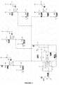
- the operating principle of the present invention is symbolized; according to this operating principle the HDMI ports are connected to the microprocessor port by means of a circuit; the present invention is exemplified by means of a system with 4 HDMI ports in order to make clear the benefits of this invention; so, when any external device is connected to the HDMI 1, HDMI 2, HDMI 3, or HDMI 4 ports of the system, the duty cycle value on the microprocessor's port shall change so that the microprocessor shall be able to detect as to which port is connected with a device according to the duty cycle alteration values previously stored on the microprocessor; likewise, it shall also be identifiable that no external device is connected to the system thanks to the present invention.
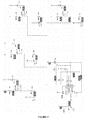
- a 555D integrated timer circuit is used in the "astable mode" for generating the duty cycle alteration signal in figures 3 , 5 , and 7 ; the purpose of the integrated timer circuit is to change the duty cycle depending on the values of capacitors and resistors used; the change in resistance at the "DISCHARGE” input of the integrated circuit changes the duty cycle at the "OUTPUT”.
- the "OUTPUT" of the 555D integrated circuit is connected to the microprocessor of the system; the 10000K resistor indicated as R3 in figures 3 , 5 , and 7 symbolizes the internal resistance of the microprocessor's connected port.
- the gates of the transistors M1, M9, M10, and M11 are connected to the ports HDMI 1, HDMI 2, HDMI 3, or HDMI 4 respectively in figures 3 , 5 , and 7 ; these transistors are selected among FET (field-effect transistors )for not drawing any currents.
- the gate sections of the transistors M1, M9, M10 and M11 are connected so as to switch the relevant transistor into conduction once any external device is connected to the system.
- any external device is connected to any of four HDMI ports in the system, one of the transistors M1, M9, M10, or M11 shall be switched to conduction, the resistors connected to the source and the resistors connected to the drain of these transistors shall vary the impedance at the "DISCHARGE” input at the 555D circuit, so that the impedance change at the "DISCHARGE” input will vary the duty cycle of the "OUTPUT” as required by the characteristics of the 555D circuit, and this duty cycle change will be detected by the microprocessor connected to the "OUTPUT", thus it shall become possible to determine as to which ports of the system is/are connected with external device/devices.
- a table In order to identify the HDMI ports with external device(s) connected, a table must be prepared to the software side controlling the microprocessor port into which the output of the duty timer enters. It must be written in this table as to which duty cycle value shall mean the presence of an external device connection at which HDMI port; for this purpose, a table like the one given in Figure 9 is maintained in the system on a nonvolatile memory; this memory may be a part of the microprocessor's internal memory.
- the reason why zero V value is seen on the gates of transistors M1, M9, M10, and M11 is that no external device is connected to none of HDMI ports in this instance; if, however, any external device is connected to the system, this device shall raise the voltage difference from 0 to 5V at the gate of any of transistors M1, M9, M10, and M11 by means of the 5V potential difference of itself so as to switch that transistor into conduction, and shall change the system's resistance and the duty cycle at the output of the circuit that controls the duty cycle.
- an external device is connected to one HDMI port and such externally-connected device creates a 5V potential difference at the gate of the transistor M1 as required by the characteristic of the HDMI port; in this instance, the reason why zero V is seen here at the gates of transistors M9, M10, and M11, is that no external devices are connected to the ports, except the port to which the transistor M1 is coupled.
- the external device connected to the port which is coupled to the transistor M1 is attached to the transistor M1 together with its 5V potential difference, it raises the voltage difference at the gate of the transistor M1 from 0 to 5V and switches the transistor into conduction.
- the transistor M1 is switched into conduction; the resistor R8 - which is open circuit as the transistor M1 is closed- is included into the impedance seen at the "DISCHARGE” input of the 555D integrated circuit together with the conduction of the transistor M1; the impedance value seen at this input is altered, and the duty cycle at the "OUTPUT" of the 555D integrated circuit is changed, since the impedance value of the "DISCHARGE” input is altered as required by the characteristic of said 555D integrated circuit.
- the microprocessor detects the change in the duty cycle and concludes that an external device is now connected to the HDMI port to which the transistor M1 is coupled.
- external devices are connected to all four HDMI ports of the system and such externally-connected devices has generated a 5V potential difference at the gates of transistors M1, M9, M10, and M11, as required by the characteristics of HDMI ports, so that these four transistors are set to conduct.
- the resistors R8, R17, R19, and R21 at the sources which are open as the transistors M1, M9, M10, and M11 respectively are in interruption are included in the impedance seen at the "DISCHARGE” input of the 555D integrated circuit once these transistors start conducting, the value of the impedance seen at this input is changed, and the duty cycle at the "OUTPUT" is altered as well, since the impedance of the "DISCHARGE” input is changed, as required by the characteristic of said 555D integrated circuit. Thanks to the duty cycle alteration tables previously loaded onto the microprocessor, the microprocessor detects the change in the duty cycle and concludes that to all HDMI ports are connected with one external device.
- Table 9 The table showing the probability that all ports are open or closed in this illustrative example and the time at which the duty cycle is at logic 1 for these instances is given in Table 9.
- the values shown in the table of Figure 9 as "1" are logic 1, and those indicated as “0” are logic 0; in instances in which HDMI ports are assumed to be as logic 1, it is concluded that external devices are connected to those ports.
- resistors R4, R8, R18, R17, R20, R19, R22, R21 coupled to transistors M1, M9, M10, and M11 in figures 3 , 5 , and 7 , any such alteration influencing the duty cycle's variation.
Landscapes
- Engineering & Computer Science (AREA)
- Multimedia (AREA)
- Signal Processing (AREA)
- Two-Way Televisions, Distribution Of Moving Picture Or The Like (AREA)
- Information Transfer Systems (AREA)
Applications Claiming Priority (1)
| Application Number | Priority Date | Filing Date | Title |
|---|---|---|---|
| TR2007/05888A TR200705888A2 (tr) | 2007-08-24 | 2007-08-24 | HDMI portlarının kullanımı için verimli bir metot ve devre |
Publications (3)
| Publication Number | Publication Date |
|---|---|
| EP2028854A2 true EP2028854A2 (de) | 2009-02-25 |
| EP2028854A3 EP2028854A3 (de) | 2009-04-08 |
| EP2028854B1 EP2028854B1 (de) | 2011-07-27 |
Family
ID=40019397
Family Applications (1)
| Application Number | Title | Priority Date | Filing Date |
|---|---|---|---|
| EP08162798A Active EP2028854B1 (de) | 2007-08-24 | 2008-08-22 | Effizientes Verfahren und Schaltung zur Verwendung von HDMI-Ports |
Country Status (3)
| Country | Link |
|---|---|
| EP (1) | EP2028854B1 (de) |
| AT (1) | ATE518367T1 (de) |
| TR (1) | TR200705888A2 (de) |
Cited By (4)
| Publication number | Priority date | Publication date | Assignee | Title |
|---|---|---|---|---|
| GB2480133A (en) * | 2010-05-06 | 2011-11-09 | Intel Corp | Connected HDMI device detection using a pulsed HPD signal |
| CN105893203A (zh) * | 2016-03-30 | 2016-08-24 | 福州瑞芯微电子股份有限公司 | 一种cec验证方法和装置 |
| CN110913159A (zh) * | 2019-11-29 | 2020-03-24 | 京东方科技集团股份有限公司 | 数字电视机、电子设备及控制方法 |
| CN115509984A (zh) * | 2022-09-29 | 2022-12-23 | 苏州浪潮智能科技有限公司 | 一种pcie端口顺序识别系统及方法 |
Families Citing this family (2)
| Publication number | Priority date | Publication date | Assignee | Title |
|---|---|---|---|---|
| US10019386B2 (en) | 2015-05-06 | 2018-07-10 | Nxp B.V. | Interface detection circuit |
| US9698786B2 (en) | 2015-05-29 | 2017-07-04 | Nexperia B.V. | Interface apparatus with leakage mitigation |
Citations (1)
| Publication number | Priority date | Publication date | Assignee | Title |
|---|---|---|---|---|
| US20070153132A1 (en) | 2006-01-03 | 2007-07-05 | Her-Ming Jong | Method of Intelligently Selecting a Signal Source and Associated Apparatus |
Family Cites Families (1)
| Publication number | Priority date | Publication date | Assignee | Title |
|---|---|---|---|---|
| JP2006019947A (ja) * | 2004-06-30 | 2006-01-19 | Toshiba Corp | テレビジョン受信機 |
-
2007
- 2007-08-24 TR TR2007/05888A patent/TR200705888A2/xx unknown
-
2008
- 2008-08-22 AT AT08162798T patent/ATE518367T1/de not_active IP Right Cessation
- 2008-08-22 EP EP08162798A patent/EP2028854B1/de active Active
Patent Citations (1)
| Publication number | Priority date | Publication date | Assignee | Title |
|---|---|---|---|---|
| US20070153132A1 (en) | 2006-01-03 | 2007-07-05 | Her-Ming Jong | Method of Intelligently Selecting a Signal Source and Associated Apparatus |
Cited By (6)
| Publication number | Priority date | Publication date | Assignee | Title |
|---|---|---|---|---|
| GB2480133A (en) * | 2010-05-06 | 2011-11-09 | Intel Corp | Connected HDMI device detection using a pulsed HPD signal |
| CN102281458A (zh) * | 2010-05-06 | 2011-12-14 | 英特尔公司 | Hdmi电缆连接装置和方法 |
| KR101333917B1 (ko) * | 2010-05-06 | 2013-11-27 | 인텔 코오퍼레이션 | Hdmi 케이블 연결 장치 및 방법 |
| CN105893203A (zh) * | 2016-03-30 | 2016-08-24 | 福州瑞芯微电子股份有限公司 | 一种cec验证方法和装置 |
| CN110913159A (zh) * | 2019-11-29 | 2020-03-24 | 京东方科技集团股份有限公司 | 数字电视机、电子设备及控制方法 |
| CN115509984A (zh) * | 2022-09-29 | 2022-12-23 | 苏州浪潮智能科技有限公司 | 一种pcie端口顺序识别系统及方法 |
Also Published As
| Publication number | Publication date |
|---|---|
| EP2028854B1 (de) | 2011-07-27 |
| TR200705888A2 (tr) | 2009-03-23 |
| EP2028854A3 (de) | 2009-04-08 |
| ATE518367T1 (de) | 2011-08-15 |
Similar Documents
| Publication | Publication Date | Title |
|---|---|---|
| EP2028854B1 (de) | Effizientes Verfahren und Schaltung zur Verwendung von HDMI-Ports | |
| EP1782224B1 (de) | Vorrichtung und verfahren zur ermöglichung von digitaler und analoger datenkommunikation über einen datenbus | |
| US7495356B2 (en) | Dual power supply system | |
| US8760219B2 (en) | Current providing circuit and voltage providing circuit | |
| US7839026B2 (en) | Power discharge control system | |
| US20080290732A1 (en) | Power switch system | |
| US20120159207A1 (en) | Power management device and method thereof | |
| WO2009126241A9 (en) | Technique for combining in-rush current limiting and short circuit current limiting | |
| US10845626B2 (en) | Display apparatus and headphone control circuit thereof | |
| JP2008202997A (ja) | 温度検出回路 | |
| US8184488B2 (en) | Systems and methods for controlling integrated circuit operation with below ground pin voltage | |
| US20100302699A1 (en) | Electrical fuse circuit and method of operating the same | |
| US20110031905A1 (en) | Single General Purpose Input/Output (GPIO) Pin Motor Control Circuit | |
| US6876400B2 (en) | Apparatus and method for protecting a memory sharing signal control lines with other circuitry | |
| KR100822321B1 (ko) | 보안 디바이스에 변화하는 바이어스 전압을 제공하기 위한 디바이스 및 방법 | |
| US11031934B2 (en) | Connection circuit and connection method thereof | |
| US9946250B2 (en) | Servo actuator default disconnected ID setting method for servo controlling system | |
| US7932628B2 (en) | Control device with terminal 15—holding circuit | |
| CN113615027B (zh) | 供电控制装置、开路探测方法及计算机程序 | |
| JP4260632B2 (ja) | 信号制御ラインを共有する装置および方法 | |
| EP2302467A2 (de) | Bilderzeugungsvorrichtung und Steuerverfahren dafür | |
| KR101437165B1 (ko) | 에이치디엠아이 입출력 포트 자동 설정장치 및 방법 | |
| KR100903903B1 (ko) | 비디오 스위칭 시스템 | |
| US20190214978A1 (en) | Output circuit and output method | |
| US20240361817A1 (en) | Power supply control device and power supply control method |
Legal Events
| Date | Code | Title | Description |
|---|---|---|---|
| PUAI | Public reference made under article 153(3) epc to a published international application that has entered the european phase |
Free format text: ORIGINAL CODE: 0009012 |
|
| 17P | Request for examination filed |
Effective date: 20080911 |
|
| AK | Designated contracting states |
Kind code of ref document: A2 Designated state(s): AT BE BG CH CY CZ DE DK EE ES FI FR GB GR HR HU IE IS IT LI LT LU LV MC MT NL NO PL PT RO SE SI SK TR |
|
| AX | Request for extension of the european patent |
Extension state: AL BA MK RS |
|
| PUAL | Search report despatched |
Free format text: ORIGINAL CODE: 0009013 |
|
| AK | Designated contracting states |
Kind code of ref document: A3 Designated state(s): AT BE BG CH CY CZ DE DK EE ES FI FR GB GR HR HU IE IS IT LI LT LU LV MC MT NL NO PL PT RO SE SI SK TR |
|
| AX | Request for extension of the european patent |
Extension state: AL BA MK RS |
|
| AKX | Designation fees paid |
Designated state(s): AT BE BG CH CY CZ DE DK EE ES FI FR GB GR HR HU IE IS IT LI LT LU LV MC MT NL NO PL PT RO SE SI SK TR |
|
| GRAP | Despatch of communication of intention to grant a patent |
Free format text: ORIGINAL CODE: EPIDOSNIGR1 |
|
| GRAC | Information related to communication of intention to grant a patent modified |
Free format text: ORIGINAL CODE: EPIDOSCIGR1 |
|
| GRAS | Grant fee paid |
Free format text: ORIGINAL CODE: EPIDOSNIGR3 |
|
| GRAA | (expected) grant |
Free format text: ORIGINAL CODE: 0009210 |
|
| AK | Designated contracting states |
Kind code of ref document: B1 Designated state(s): AT BE BG CH CY CZ DE DK EE ES FI FR GB GR HR HU IE IS IT LI LT LU LV MC MT NL NO PL PT RO SE SI SK TR |
|
| REG | Reference to a national code |
Ref country code: GB Ref legal event code: FG4D |
|
| REG | Reference to a national code |
Ref country code: CH Ref legal event code: EP |
|
| REG | Reference to a national code |
Ref country code: DE Ref legal event code: R096 Ref document number: 602008008506 Country of ref document: DE Effective date: 20110915 |
|
| REG | Reference to a national code |
Ref country code: NL Ref legal event code: VDEP Effective date: 20110727 |
|
| PG25 | Lapsed in a contracting state [announced via postgrant information from national office to epo] |
Ref country code: MT Free format text: LAPSE BECAUSE OF FAILURE TO SUBMIT A TRANSLATION OF THE DESCRIPTION OR TO PAY THE FEE WITHIN THE PRESCRIBED TIME-LIMIT Effective date: 20110727 |
|
| REG | Reference to a national code |
Ref country code: AT Ref legal event code: MK05 Ref document number: 518367 Country of ref document: AT Kind code of ref document: T Effective date: 20110727 |
|
| PG25 | Lapsed in a contracting state [announced via postgrant information from national office to epo] |
Ref country code: PT Free format text: LAPSE BECAUSE OF FAILURE TO SUBMIT A TRANSLATION OF THE DESCRIPTION OR TO PAY THE FEE WITHIN THE PRESCRIBED TIME-LIMIT Effective date: 20111128 Ref country code: IS Free format text: LAPSE BECAUSE OF FAILURE TO SUBMIT A TRANSLATION OF THE DESCRIPTION OR TO PAY THE FEE WITHIN THE PRESCRIBED TIME-LIMIT Effective date: 20111127 Ref country code: HR Free format text: LAPSE BECAUSE OF FAILURE TO SUBMIT A TRANSLATION OF THE DESCRIPTION OR TO PAY THE FEE WITHIN THE PRESCRIBED TIME-LIMIT Effective date: 20110727 Ref country code: NO Free format text: LAPSE BECAUSE OF FAILURE TO SUBMIT A TRANSLATION OF THE DESCRIPTION OR TO PAY THE FEE WITHIN THE PRESCRIBED TIME-LIMIT Effective date: 20111027 Ref country code: FI Free format text: LAPSE BECAUSE OF FAILURE TO SUBMIT A TRANSLATION OF THE DESCRIPTION OR TO PAY THE FEE WITHIN THE PRESCRIBED TIME-LIMIT Effective date: 20110727 Ref country code: NL Free format text: LAPSE BECAUSE OF FAILURE TO SUBMIT A TRANSLATION OF THE DESCRIPTION OR TO PAY THE FEE WITHIN THE PRESCRIBED TIME-LIMIT Effective date: 20110727 Ref country code: LT Free format text: LAPSE BECAUSE OF FAILURE TO SUBMIT A TRANSLATION OF THE DESCRIPTION OR TO PAY THE FEE WITHIN THE PRESCRIBED TIME-LIMIT Effective date: 20110727 Ref country code: SE Free format text: LAPSE BECAUSE OF FAILURE TO SUBMIT A TRANSLATION OF THE DESCRIPTION OR TO PAY THE FEE WITHIN THE PRESCRIBED TIME-LIMIT Effective date: 20110727 Ref country code: BE Free format text: LAPSE BECAUSE OF FAILURE TO SUBMIT A TRANSLATION OF THE DESCRIPTION OR TO PAY THE FEE WITHIN THE PRESCRIBED TIME-LIMIT Effective date: 20110727 |
|
| PG25 | Lapsed in a contracting state [announced via postgrant information from national office to epo] |
Ref country code: PL Free format text: LAPSE BECAUSE OF FAILURE TO SUBMIT A TRANSLATION OF THE DESCRIPTION OR TO PAY THE FEE WITHIN THE PRESCRIBED TIME-LIMIT Effective date: 20110727 Ref country code: SI Free format text: LAPSE BECAUSE OF FAILURE TO SUBMIT A TRANSLATION OF THE DESCRIPTION OR TO PAY THE FEE WITHIN THE PRESCRIBED TIME-LIMIT Effective date: 20110727 Ref country code: GR Free format text: LAPSE BECAUSE OF FAILURE TO SUBMIT A TRANSLATION OF THE DESCRIPTION OR TO PAY THE FEE WITHIN THE PRESCRIBED TIME-LIMIT Effective date: 20111028 Ref country code: CY Free format text: LAPSE BECAUSE OF FAILURE TO SUBMIT A TRANSLATION OF THE DESCRIPTION OR TO PAY THE FEE WITHIN THE PRESCRIBED TIME-LIMIT Effective date: 20110727 Ref country code: AT Free format text: LAPSE BECAUSE OF FAILURE TO SUBMIT A TRANSLATION OF THE DESCRIPTION OR TO PAY THE FEE WITHIN THE PRESCRIBED TIME-LIMIT Effective date: 20110727 Ref country code: LV Free format text: LAPSE BECAUSE OF FAILURE TO SUBMIT A TRANSLATION OF THE DESCRIPTION OR TO PAY THE FEE WITHIN THE PRESCRIBED TIME-LIMIT Effective date: 20110727 |
|
| PG25 | Lapsed in a contracting state [announced via postgrant information from national office to epo] |
Ref country code: MC Free format text: LAPSE BECAUSE OF NON-PAYMENT OF DUE FEES Effective date: 20110831 |
|
| PG25 | Lapsed in a contracting state [announced via postgrant information from national office to epo] |
Ref country code: CZ Free format text: LAPSE BECAUSE OF FAILURE TO SUBMIT A TRANSLATION OF THE DESCRIPTION OR TO PAY THE FEE WITHIN THE PRESCRIBED TIME-LIMIT Effective date: 20110727 Ref country code: SK Free format text: LAPSE BECAUSE OF FAILURE TO SUBMIT A TRANSLATION OF THE DESCRIPTION OR TO PAY THE FEE WITHIN THE PRESCRIBED TIME-LIMIT Effective date: 20110727 |
|
| REG | Reference to a national code |
Ref country code: IE Ref legal event code: MM4A |
|
| PG25 | Lapsed in a contracting state [announced via postgrant information from national office to epo] |
Ref country code: RO Free format text: LAPSE BECAUSE OF FAILURE TO SUBMIT A TRANSLATION OF THE DESCRIPTION OR TO PAY THE FEE WITHIN THE PRESCRIBED TIME-LIMIT Effective date: 20110727 Ref country code: EE Free format text: LAPSE BECAUSE OF FAILURE TO SUBMIT A TRANSLATION OF THE DESCRIPTION OR TO PAY THE FEE WITHIN THE PRESCRIBED TIME-LIMIT Effective date: 20110727 |
|
| PLBE | No opposition filed within time limit |
Free format text: ORIGINAL CODE: 0009261 |
|
| STAA | Information on the status of an ep patent application or granted ep patent |
Free format text: STATUS: NO OPPOSITION FILED WITHIN TIME LIMIT |
|
| PG25 | Lapsed in a contracting state [announced via postgrant information from national office to epo] |
Ref country code: DK Free format text: LAPSE BECAUSE OF FAILURE TO SUBMIT A TRANSLATION OF THE DESCRIPTION OR TO PAY THE FEE WITHIN THE PRESCRIBED TIME-LIMIT Effective date: 20110727 |
|
| 26N | No opposition filed |
Effective date: 20120502 |
|
| PG25 | Lapsed in a contracting state [announced via postgrant information from national office to epo] |
Ref country code: IE Free format text: LAPSE BECAUSE OF NON-PAYMENT OF DUE FEES Effective date: 20110822 |
|
| REG | Reference to a national code |
Ref country code: DE Ref legal event code: R097 Ref document number: 602008008506 Country of ref document: DE Effective date: 20120502 |
|
| REG | Reference to a national code |
Ref country code: CH Ref legal event code: PL |
|
| PG25 | Lapsed in a contracting state [announced via postgrant information from national office to epo] |
Ref country code: LI Free format text: LAPSE BECAUSE OF NON-PAYMENT OF DUE FEES Effective date: 20120831 Ref country code: ES Free format text: LAPSE BECAUSE OF FAILURE TO SUBMIT A TRANSLATION OF THE DESCRIPTION OR TO PAY THE FEE WITHIN THE PRESCRIBED TIME-LIMIT Effective date: 20111107 Ref country code: CH Free format text: LAPSE BECAUSE OF NON-PAYMENT OF DUE FEES Effective date: 20120831 |
|
| PG25 | Lapsed in a contracting state [announced via postgrant information from national office to epo] |
Ref country code: LU Free format text: LAPSE BECAUSE OF NON-PAYMENT OF DUE FEES Effective date: 20110822 |
|
| PG25 | Lapsed in a contracting state [announced via postgrant information from national office to epo] |
Ref country code: BG Free format text: LAPSE BECAUSE OF FAILURE TO SUBMIT A TRANSLATION OF THE DESCRIPTION OR TO PAY THE FEE WITHIN THE PRESCRIBED TIME-LIMIT Effective date: 20111027 |
|
| PG25 | Lapsed in a contracting state [announced via postgrant information from national office to epo] |
Ref country code: HU Free format text: LAPSE BECAUSE OF FAILURE TO SUBMIT A TRANSLATION OF THE DESCRIPTION OR TO PAY THE FEE WITHIN THE PRESCRIBED TIME-LIMIT Effective date: 20110727 |
|
| REG | Reference to a national code |
Ref country code: FR Ref legal event code: PLFP Year of fee payment: 8 |
|
| REG | Reference to a national code |
Ref country code: FR Ref legal event code: PLFP Year of fee payment: 9 |
|
| REG | Reference to a national code |
Ref country code: FR Ref legal event code: PLFP Year of fee payment: 10 |
|
| REG | Reference to a national code |
Ref country code: FR Ref legal event code: PLFP Year of fee payment: 11 |
|
| PGFP | Annual fee paid to national office [announced via postgrant information from national office to epo] |
Ref country code: TR Payment date: 20250820 Year of fee payment: 18 |
|
| PGFP | Annual fee paid to national office [announced via postgrant information from national office to epo] |
Ref country code: DE Payment date: 20251021 Year of fee payment: 18 |
|
| PGFP | Annual fee paid to national office [announced via postgrant information from national office to epo] |
Ref country code: GB Payment date: 20251021 Year of fee payment: 18 |
|
| PGFP | Annual fee paid to national office [announced via postgrant information from national office to epo] |
Ref country code: IT Payment date: 20251024 Year of fee payment: 18 |
|
| PGFP | Annual fee paid to national office [announced via postgrant information from national office to epo] |
Ref country code: FR Payment date: 20251029 Year of fee payment: 18 |