EP2030294B1 - Lasergeräte mit verstärkungsmedien im gegenphasigen modus - Google Patents
Lasergeräte mit verstärkungsmedien im gegenphasigen modus Download PDFInfo
- Publication number
- EP2030294B1 EP2030294B1 EP07795355.2A EP07795355A EP2030294B1 EP 2030294 B1 EP2030294 B1 EP 2030294B1 EP 07795355 A EP07795355 A EP 07795355A EP 2030294 B1 EP2030294 B1 EP 2030294B1
- Authority
- EP
- European Patent Office
- Prior art keywords
- lateral
- mirror
- gain
- mirrors
- coupler
- Prior art date
- Legal status (The legal status is an assumption and is not a legal conclusion. Google has not performed a legal analysis and makes no representation as to the accuracy of the status listed.)
- Active
Links
Images


Classifications
-
- H—ELECTRICITY
- H01—ELECTRIC ELEMENTS
- H01S—DEVICES USING THE PROCESS OF LIGHT AMPLIFICATION BY STIMULATED EMISSION OF RADIATION [LASER] TO AMPLIFY OR GENERATE LIGHT; DEVICES USING STIMULATED EMISSION OF ELECTROMAGNETIC RADIATION IN WAVE RANGES OTHER THAN OPTICAL
- H01S3/00—Lasers, i.e. devices using stimulated emission of electromagnetic radiation in the infrared, visible or ultraviolet wave range
- H01S3/05—Construction or shape of optical resonators; Accommodation of active medium therein; Shape of active medium
- H01S3/06—Construction or shape of active medium
- H01S3/0627—Construction or shape of active medium the resonator being monolithic, e.g. microlaser
-
- H—ELECTRICITY
- H01—ELECTRIC ELEMENTS
- H01S—DEVICES USING THE PROCESS OF LIGHT AMPLIFICATION BY STIMULATED EMISSION OF RADIATION [LASER] TO AMPLIFY OR GENERATE LIGHT; DEVICES USING STIMULATED EMISSION OF ELECTROMAGNETIC RADIATION IN WAVE RANGES OTHER THAN OPTICAL
- H01S3/00—Lasers, i.e. devices using stimulated emission of electromagnetic radiation in the infrared, visible or ultraviolet wave range
- H01S3/05—Construction or shape of optical resonators; Accommodation of active medium therein; Shape of active medium
- H01S3/06—Construction or shape of active medium
- H01S3/063—Waveguide lasers, i.e. whereby the dimensions of the waveguide are of the order of the light wavelength
- H01S3/0632—Thin film lasers in which light propagates in the plane of the thin film
- H01S3/0635—Thin film lasers in which light propagates in the plane of the thin film provided with a periodic structure, e.g. using distributed feed-back, grating couplers
-
- H—ELECTRICITY
- H01—ELECTRIC ELEMENTS
- H01S—DEVICES USING THE PROCESS OF LIGHT AMPLIFICATION BY STIMULATED EMISSION OF RADIATION [LASER] TO AMPLIFY OR GENERATE LIGHT; DEVICES USING STIMULATED EMISSION OF ELECTROMAGNETIC RADIATION IN WAVE RANGES OTHER THAN OPTICAL
- H01S3/00—Lasers, i.e. devices using stimulated emission of electromagnetic radiation in the infrared, visible or ultraviolet wave range
- H01S3/05—Construction or shape of optical resonators; Accommodation of active medium therein; Shape of active medium
- H01S3/08—Construction or shape of optical resonators or components thereof
- H01S3/081—Construction or shape of optical resonators or components thereof comprising three or more reflectors
- H01S3/082—Construction or shape of optical resonators or components thereof comprising three or more reflectors defining a plurality of resonators, e.g. for mode selection or suppression
-
- H—ELECTRICITY
- H01—ELECTRIC ELEMENTS
- H01S—DEVICES USING THE PROCESS OF LIGHT AMPLIFICATION BY STIMULATED EMISSION OF RADIATION [LASER] TO AMPLIFY OR GENERATE LIGHT; DEVICES USING STIMULATED EMISSION OF ELECTROMAGNETIC RADIATION IN WAVE RANGES OTHER THAN OPTICAL
- H01S3/00—Lasers, i.e. devices using stimulated emission of electromagnetic radiation in the infrared, visible or ultraviolet wave range
- H01S3/23—Arrangements of two or more lasers not provided for in groups H01S3/02 - H01S3/22, e.g. tandem arrangements of separate active media
- H01S3/2308—Amplifier arrangements, e.g. MOPA
-
- H—ELECTRICITY
- H01—ELECTRIC ELEMENTS
- H01S—DEVICES USING THE PROCESS OF LIGHT AMPLIFICATION BY STIMULATED EMISSION OF RADIATION [LASER] TO AMPLIFY OR GENERATE LIGHT; DEVICES USING STIMULATED EMISSION OF ELECTROMAGNETIC RADIATION IN WAVE RANGES OTHER THAN OPTICAL
- H01S5/00—Semiconductor lasers
- H01S5/005—Optical components external to the laser cavity, specially adapted therefor, e.g. for homogenisation or merging of the beams or for manipulating laser pulses, e.g. pulse shaping
- H01S5/0071—Optical components external to the laser cavity, specially adapted therefor, e.g. for homogenisation or merging of the beams or for manipulating laser pulses, e.g. pulse shaping for beam steering, e.g. using a mirror outside the cavity to change the beam direction
-
- H—ELECTRICITY
- H01—ELECTRIC ELEMENTS
- H01S—DEVICES USING THE PROCESS OF LIGHT AMPLIFICATION BY STIMULATED EMISSION OF RADIATION [LASER] TO AMPLIFY OR GENERATE LIGHT; DEVICES USING STIMULATED EMISSION OF ELECTROMAGNETIC RADIATION IN WAVE RANGES OTHER THAN OPTICAL
- H01S5/00—Semiconductor lasers
- H01S5/20—Structure or shape of the semiconductor body to guide the optical wave ; Confining structures perpendicular to the optical axis, e.g. index or gain guiding, stripe geometry, broad area lasers, gain tailoring, transverse or lateral reflectors, special cladding structures, MQW barrier reflection layers
- H01S5/2036—Broad area lasers
Definitions
- the present invention relates to a basic gain medium enclosure for laser devices that comprises two parallel lateral mirrors which geometrically define the extent of the gain medium enclosure and which allow the formation of lateral stationary sinusoidal waves.
- lateral field distribution For each resonator there is a multitude of lateral field distributions (or configurations), named lateral modes, each characterized by the zeros and maxima of the field intensity.
- the fundamental mode has no zero in lateral cross section and the field in concentrated toward the axis of propagation.
- the fundamental mode of the Fabry-Perot resonator for cylindrical shape lasers has a Gaussian cylindrical type of lateral field distribution.
- the gain medium, superimposed over the field distribution, provides the necessary power for laser oscillation in spite of internal or mirror losses.
- Gain and/or array elements are linearly distributed in semiconductor or fiber laser arrays or might further be circularly or lattice distributed in fiber array. Usually the arrays have a larger lateral spatial extent than a single element laser and this further multiply the possible field configurations. Those configurations that have intensity peaks at the gain locations are preferred for oscillations since they have best coupling between the field intensity and the gain and low threshold. Linearly distributed arrays usually are designed (or intended) for the in phase mode of operation, i. e., each intensity peak coupled with a gain element to be in phase with any other peak coupled with gain elements. Nevertheless, most often, arrays oscillate in the out of phase mode, where each intensity peak coupled with a gain element is in out of phase with its adjacent peaks coupled with gain elements.
- the field configurations for array are named super-modes. This name came as an extension for the field configuration of a single element, which is a mode. In the week coupling case, the modes of individual elements couple together with different phases, forming the super-mode. In the strong coupling case, the name super-mode looses this semantic sense: the field configuration is holistic, depends on the entire extent of the refractive index profile and might not be spatially correlated with gain positions.
- US 2002/122455 A1 discloses a laser device comprising a folded cavity design with a rectangular enclosure and a pair of external mirrors.
- the device according to the present invention is of long longitudinal spatial extent in one direction, a wide lateral spatial extent in an other perpendicular direction and a restricted transversal spatial extent in a third direction perpendicular on the former two, with uniform lateral and longitudinal distribution of the refractive indexes, such that the radiation propagate in the longitudinal-lateral plane as plane waves; in between its longitudinal and lateral spatial extents, the device has a gain medium; the gain medium is geometrically enclosed by a mirror configuration formed by two lateral mirror at the ends of the lateral spatial extent, such that inclined plane waves that propagate between the two lateral mirrors form pure sinusoidal stationary waves in a lateral cross section.
- the device In one set-up, intended to form a closed optical path, the device has a back mirror at one end of the longitudinal spatial extent a semi-transparent mirror at the second end of the longitudinal spatial extent such that the far field consists of two diffraction-limited lobes.
- Mechanisms external to these devices can transform the far field with two diffraction limited lobes into a single diffraction limited lobe.
- the devices according to the invention can be formed in epitaxial structure of a semiconductor laser or in a layered structure of a ribbon laser.
- a ribbon laser can be made, for example, from glass materials that include gain cores or gain sheets.
- a ribbon laser can have on one side or both transversal sides, top and bottom, thicker layers for optical pumping. In a fiber analogy, these layers are named claddings.
- Perpendicular to the layered structure is a transversal direction x. In the plane of the layered structure there is a longitudinal direction z and a lateral direction y. The directions x, y, and z are perpendicular to each other.
- the transversal extent of the layered structure is spatially limited and the layers give a convex shape to the refractive index profile as a function of the x coordinate.
- this refractive index profile only a single transversal field distribution E(x) is favored by the transversal gain and losses distribution. It might be assumed that this field distribution has a single peak and no zeros and that it is the fundamental transversal field distribution.
- FIG. 1 represents a lateral cross section of the basic elements of the devices according with the invention in the y-z plane.
- the gain medium has a rectangular shape.
- the refractive index has no dependence on y and z, it is uniform in these directions.
- the propagation in the y-z direction is characterized by an effective refractive index n.
- 2 ⁇ n/ ⁇
- the rectangular gain medium is enclosed on its sides by two parallel, lateral mirrors 1 and 2 perpendicular to the lateral direction y and separated by a lateral spatial extent w.
- the two lateral, parallel mirrors geometrically determine the extent of the rectangular enclosure. They form the I I shaped mirror configuration.
- a back mirror 3 perpendicular to the longitudinal direction z might enclose the gain medium on one side of its longitudinal extent in z direction.
- the I I shaped mirror configuration, i. e. mirrors 1 and 2, plus mirror 3 form a U shaped mirror configuration.
- a virtual input-output boundary 4 closes the ends of the mirror 1 and 2 opposite to the back mirror 3.
- Boundary 4 is separated by a distance L from the back mirror 3.
- the mirrors can have a phase shift of 0 or ⁇ rad.
- all mirror have a phase shift of ⁇ rad, but 0 rad shift is not excluded.
- FIG. 2 presents the first embodiment of a device using the U-shaped mirror configuration.
- the first embodiment device is named the Y-resonator.
- the U-shaped mirror configuration geometrically encloses the gain medium of a laser oscillator.
- the gain medium is closed with a front longitudinal mirror 5 at the location of the virtual boundary 4.
- Mirror 5 is semitransparent to allow for the partial radiation exit.
- ⁇ is the free space wavelength.
- the oscillation frequency v and the free space ⁇ can be selected by a gain-loss selection mechanism, for example with a Bragg reflector as the back mirror.
- the lateral wave number q can be selected by another gain-loss mechanism, for example a periodic gain with a lateral period ⁇ q .
- the gain peaks should be located at the intensity maxima of the sinusoidal field distribution of the preferred mode.
- this embodiment there are essentially three light paths, one inside the U-shaped mirror configuration and two external, symmetrically inclined relative to the first one. These paths are arranged as a Y shape. That is why this resonator is named the Y-resonator.
- the Y resonator has two diffraction-limited beams separated by 20 angle.
- FIG. 3 is presented simple optical system that uses two mirrors 6 and 7 to rearrange the beams parallel and close to each other.
- the resulting beam quality measured by the Beam Parameter Product is only 3 times larger than that of single diffraction limited beam.
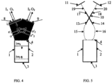
- FIG. 4 presents the second embodiment of a device using the U-shaped mirror configuration.
- the second embodiment device is named the ⁇ -resonator (accent Y resonator).
- the U-shaped mirror configuration geometrically encloses the gain medium of a laser oscillator. Optical paths are closed on one side with an inclined external mirror 8 and on the other side with an opposite inclined external mirror 9. Mirrors 8 and 9 capture and reflect back exactly in the same directions, the inclined plane wave beams of the U-shaped mirror configuration.
- the virtual boundary 4 can be replaced by a low reflectance mirror 5. In this case, between pair of mirrors (5, 3), (5, 8) and (5, 9) three coupled cavities are formed.
- a plane wave i 1 of finite extent at input I 1 reaching and exactly filling the aperture of the virtual boundary 4, separates in three parts: a reflected wave o' 2 toward the output O 2 , one reflected o' 1 back toward the output O 1 and an inside wave iw b that couples with one of the modal configurations of the U-shaped mirror configuration.
- the iw b wave propagates longitudinally toward the back mirror 3. After reflection on mirror 3, the wave propagates forward as a wave iw f .
- the iw r wave separates in two waves o" 1 and o" 2 in directions O 1 and O 2 .
- the iw r wave separates in two waves o" 1 and o" 2 in directions O 1 and O 2 .
- a threshold formula can be found for the Y - resonator, which essentially consists of the three paths: an external path from the mirror 8 to the U-shaped mirror configuration, an internal path inside the U-shaped mirror configuration and a second external path from the U-shaped mirror configuration to the external mirror 9.
- the mirror 8 can have close to 100% reflectance and is called the return mirror, while mirror 9 can have close to 0% reflectance, including 0 reflectance and is called the output coupler.
- the T matrix analysis shows that the ⁇ - resonator has somewhat lower threshold then a Fabry-Perot resonator and also has lower slope efficiency. This can be explained by the semi-closed loop between the return mirror and the back mirror of the array cavity. This loop reduces the gain necessary for threshold but also reduces the power at the output coupler due to the absorption of the light traveling forth and back between the two high reflectance mirrors.
- the ⁇ - resonator transforms the two diffraction-limited beams of a U shaped mirror configuration into a single diffraction limited beam.
- FIG. 5 presents the third embodiment of a device using the U-shaped mirror configuration.
- the third embodiment device is named the YX-resonator.
- the U-shaped mirror configuration geometrically encloses the gain medium of a laser oscillator. Optical paths are closed with an external 3db coupler 10, an output coupler 11 and a full loss exit coupler 12. The two beams from the U-shaped mirror configuration are guided to the first two branches 13 and 14 of the 3db coupler along two optical paths 15 and 16.
- a 3db coupler can be implemented in fiber optic design. It can be also implemented with a beam splitter such as a cube beam splitter.
- the 3db coupler essentially consists of four input-output branches. The easiest way to explain such type of coupler is to assume that, if two equal, coherent, in-phase beams enter two selected branches 13 and 14 the coherent addition exits at a third branch 17 and the null coherent subtraction exists at the forth branch 18. Other phase arrangements are possible and their effects on the operation of the resonator are similar.
- the 3db coupler can have a shorthand representation as the X letter and its combination with the Y-resonator configuration can have the shorthand as the YX letters combination.
- An optical path 19 exists between the X coupler branch 17 and the output coupler 11.
- Another optical path 20 exists between the X coupler branch 18 and the full loss exit coupler 12.
- the YX-resonator takes its feedback from the output coupler 11 through coupler branch 17. No feedback comes from the exit coupler 12 and coupler branch 18.
- the feedback splits in two, equal-amplitude, coherent and in phase beams. These beams are conducted to the inputs of the U-shaped mirror configuration by the optical paths 15 and 16. Depending on the ⁇ value, they might not arrive in phase.
- the YX - resonator transforms the two diffraction-limited beams of a U shaped mirror configuration into a single diffraction limited beam.
- FIG. 6 shows the forth embodiment for a device of the present invention. It derives from the third embodiment and its proposed name is XYYX.
- XYYX resonator the gain medium is geometrically enclosed by the II shaped mirror configuration, i. e. by two lateral mirrors 1 and 2 and has two virtual boundaries 4 and 4'. It is closed on one side with a 3db coupler 10, an output coupler 11 and a full loss exit coupler 12 and on the other side with another 3db coupler 10', another output coupler 11' and another full loss exit coupler 12'.
- the two beams at the virtual boundary 4 are guided to the first two branches 13 and 14 of the 3db coupler along two optical paths 15 and 16.
- the two beams at the virtual boundary 4' are guided to the first two branches 13' and 14' of the 3db coupler 10' along two optical paths 15' and 16'.
- the XYYX arrangement is similar with an amplifier.
- a beam entering the branch 17' splits in to equal, coherent, in phase beams that exit at braches 13' and 14'.
- Guided by the optical paths 15' and 16' they enter the gain medium and couple with its sinusoidal preferred mode. After amplification the sinusoidal mode splits again in two beams.
- These beams are guided by the optical paths 15 and 16 to the branches 13 and 14 of the X coupler 10, add coherently and exit at the branch 17.
- the correct phasing after exiting the paths 15' and 16' or the paths 15 and 16 is not automatically reached in the amplifier mode of operation.
- the minimum threshold argument is still valid if output couplers 11 and 11' are added and the arrangement becomes an oscillator.
- the full loss couplers 12 and 12' are also necessary to avoid any undesired feedback.
- the XYYX resonator is similar with the Fabry-Perot resonator.
- the difference consists in the fact that the spatial extension of the gain medium is much larger than that of a usual single mode Fabry-Perot oscillator.
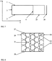
- FIG. 7 shows another device according to invention.
- a grating coupler 25 and the output coupler 26 In front of the U shaped mirror configuration that encloses the periodic gain medium there is a grating coupler 25 and the output coupler 26.
- FIG. 8 shows schematically the grating coupler.
- the grating coupler is a wide waveguide that has two lateral mirrors 27 and 28, which continue and are aligned to the lateral mirrors of the U shaped mirror configuration, an input face 29 and output face 30. It has a width w equal to the width of the U shaped mirror configuration and a length L g .
- the modes of the coupler have essentially the same lateral field distribution as the modes of the U shaped mirror configuration.
- the grating coupler has a grating 31 that induces an effective refractive index modulation ⁇ n.
- This modulation that acts as a perturbation in the propagation of the grating coupler modes and performs the coupling from the input preferred mode q of the U shaped mirror configuration into the output fundamental mode 0.
- the grating derives from a long period grating with period ⁇ g in the z direction.
- the period of a long period grating is related to the propagation constants in z direction k qz and k 0z of the mode q and, respectively, mode 0.
- k qz and k 0z are related to the lateral wavelength of these modes ⁇ q and ⁇ 0 , where ⁇ q ⁇ ⁇ 0 .
- ⁇ n sin 2 ⁇ / ⁇ g z sin 2 ⁇ / ⁇ q y
- Two gratings 32 and 33 symmetrically inclined relative to the z direction can induce a modulation of this form, as shown in FIG. 8 .
- the modulated long period grating can operate with other periodic function that modulates the effective refractive index.
- These periodic functions have Fourier components that have spatial periods ⁇ Fzi and ⁇ Fyi .
- the mode interaction will be determined by the matching Fourier components with periods ⁇ Fzn , and ⁇ Fym that match the difference in propagation constants of the two modes as in relation (8) and the lateral k qy vector of the preferred mode.
- the design of the properties of the gratings that modulate the effective refractive index in real 3D waveguide structure is the reverse process of the process that goes from a real 3D structure to 2D.
- the gratings can be implemented by modulating the optical properties of a thin grating layer of the whole layered structure.
- the grating is usually implemented by changing the optical properties of Ge doped cores.
- a sensitive grating layer parallel with the claddings should be imprinted
- the imprinting of two inclined gratings as described by equation (11) should be the method of choice.
- the imprinted geometry should be similar to the image of Fig. 9 , where the simulation of either the left or right side of relation (11) is presented.
- the simulation has a rather short ⁇ g to enhance the visual impression for two inclined gratings.
- the grating coupler thickness in the transversal, x direction can be thick and is determined by the requirements of lens intermediated transversal coupling between the laser array and the coupler. Thick couplers resemble a volume Bragg grating with two inclined gratings parallel to the x axis.
- the last important parameter of the coupler is its length L. At a given L there is a certain wavelength ⁇ for which the q mode is fully transformed to the fundamental order mode.
- the grating coupler becomes also a wavelength selector.
- the simplest way to combine the grating selector with a spatial selector is to include the grating coupler in the laser resonator, between the U shaped mirror configuration and the external coupler. The maximum resonance is achieved for the q mode that is fully transformed to the fundamental mode. Another way is to focus the transformed mode into a pinhole. The q mode fully transformed to the fundamental mode has the maximum transfer through the pinhole.
- the grating coupler can have the reverse functionality and act as a grating splitter when the fundamental mode enters one face and the preferred mode exit at the other face.
- FIG. 10 shows an arrangement of a device with a first grating coupler 33, which acts as a grating splitter, a gain medium 34, which has lateral mirror 1 and 2 and has not the back mirror 3, and a second grating coupler 35.
- This device has a fundamental mode input, a wide periodic gain medium for the propagation and amplification of the preferred mode and a fundamental mode output. If feedback is reduced by very low reflectivity of the external facets 36 and 37 of the first and second coupler, the device can operate as a laser amplifier. This amplifier can operate at high saturation output power due to its possible wide spatial extent.
- the principles of this invention are applied to layered structures such as epitaxial semiconductor layers and ribbon laser made for example from layered glass.
- the basic layered structure forms a planar waveguide that accept waves of the form given by (1).
- the lateral mirrors 1 and 2 are essential for reflecting back into the gain medium any wave that propagate at an angle relative to the longitudinal axis.
- the basic description is valid for both types of mirrors, lateral and longitudinal. The specificity for the case of lateral mirrors will be stressed when necessary.
- FIG. 11 presents one type of mirror.
- This first type is an adjacent external stack mirror that is formed external to and adjacent to one facet 41 of the layered structure. Facet 41 is perpendicular to the basic layered structure 42.
- the mirror is formed by a quarter wavelength stack of secondary alternating layers 43 and 44, made of alternating optical materials with refractive index different from each other.
- the secondary layers are perpendicular to the basic layered structure.
- An external stack is usually not very selective mirror with regard to wavelength or incidence angle due to high contrast (difference) between the refractive indexes. Nevertheless, if the contrast is very small and the external stack has a very large number of layers, its selectivity increases and the name change to volume Bragg grating. Depending on the order of refractive index values of the stack materials, an external stack can induce a 0 or ⁇ phase shift. Otherwise said an external stack can pin a node or a maximum at the interface between gain medium and the mirror structure.
- FIG. 12 presents another type of mirror.
- This type is an imprinted stack mirror that is formed internal to the layered structure 42, modifying one or a few layers. These modifications change the effective refractive index of the planar waveguide forming different segments 45 and 46 of the layered structure.
- imprinting is more usually named wafer processing. A new name is used to imagine processes that provide similar segment structures in the case of ribbons, which might be much longer and wider than a semiconductor chip.
- a virtual mirror face 47 separates the first segment from the layered structure 42 that has gain inside.
- Alternating segments are parallel to virtual mirror face 47 and have different to each other effective refractive index. They are equal in width to a quarter of the lateral or longitudinal wavelength determined relative to the effective refractive index of the preferred mode.
- These alternating segments form the imprinted stack. If an imprinted stack has a small contrast in the effective refractive index and has a larger number of segments it is more selective mirror with regards to wavelength and angle of incidence. In this case it is called a (imprinted) Bragg grating.
- an imprinted stack can induce a 0 or ⁇ phase shift. Otherwise said an imprinted stack can pin a node or a maximum at the separation line between the layered structure and the first stack segment.
- the U shaped mirror configuration of this invention works best with a periodic gain inside the planar waveguide.
- the gain elements are parallel to the lateral mirrors.
- the gain period is half the lateral wavelength of the selected, preferred mode. Due to material processing constraints, the preferred mode lateral wavelength ⁇ q is approximately one order of magnitude larger than the free space wavelength ⁇ , while its longitudinal wavelength is of the same order of magnitude with ⁇ /n.
- a lateral imprinted Bragg grating will have necessarily very wide segments, making the total width of the grating exceedingly wide.
- a longitudinal imprinted Bragg grating is of reasonable extent.
- An imprinted stack, with large contrast of the effective refractive index of its segments and with wider segments, is a good, but less selective, reflector.
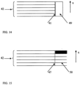
- FIG. 13 presents still another type of mirror.
- This mirror is a metallic mirror that simply has a flat metal surface 48 on the face 41 of the layered structure 42.
- FIG. 14 presents still another type of mirror. This is the two optical materials mirror and is the interface between the layered structure 42 and the material 49 (or lack of it) in outside space. This type of mirror can induce total reflection at large incidence angles.
- FIG. 15 presents still another type of mirror.
- This is the imprinted total reflection mirror. This is made by modifying in the main layered structure 42 one or a few layers to form a segment 50 in such a way that segment 50 effective refractive index is smaller than the effective refractive index of the preferred mode in the structure 42.
- the structure 42 and the segment 50 are separated by a virtual mirror face 47.
- the preferred mode propagating in structure 42 and arriving at face 47, evanescently decay in segment 50.
- Mirrors presented in FIGS. 11 to 15 are mirror adjacent to main device gain medium. As described before, most of the embodiments need also external mirrors. They can by metallic, dielectric-stack, volume Bragg gratings and diffraction gratings in Littrow arrangement. Before reaching the mirror, the light emerging from the virtual boundary 4 or the semitransparent mirror 5, should be collimated with a Fast Axis Collimator (FAC) cylindrical lens.
- FAC Fast Axis Collimator
- the FAC lens can be avoided, for example, if the return mirror 8 in the second embodiment is replaced by an inclined imprinted Bragg grating in the same, extended, integrated, transversal waveguide.
- external stack mirrors can be deposited on facets that are inclined relative to the main axis of an extended waveguide.
- inclined facets the well-known advantage of using cleaved facets is lost.
- the high contrast, short imprinted stack, the imprinted total reflection mirror and the metallic mirror are the mirrors of choice.
- the high contrast, short imprinted stacks are designed for rather large lateral wavelengths ⁇ q .
- the stack segments lateral dimensions are greater than ⁇ and it is possible to implement them with good accuracy with standard wafer processing tools.
- the imprinted total reflection mirror is the easiest to implement since does not require geometrical definition of small segments with implied accuracy. They require nevertheless, good alignment relative to the periodic gain at predetermined locations.
- the imprinted type of mirrors fit semiconductor material lasers since imprinting (i. e wafer processing) is well developed for these materials.
- a cross mode is that mode that can have total reflections at all mirrors of the U-shaped mirror configuration, including the, otherwise semitransparent, mirror 5 (or totally transparent boundary 4).
- the high contrast stack is less desirable as lateral mirror. Even for a low number of segments, the stack width can be considerable large and the radiation exiting at a non zero transversal angle do not return into the main planar waveguide. Nevertheless it might be useful if the exiting transversal angle is rather low.
- both types of Bragg grating are not desirable, even in the case of the imprinted Bragg grating, where the radiation travels in the same main planar waveguide.
- the external adjacent, high contrast, short stack and the imprinted Bragg grating are the mirrors of choice.
- the short stack has good reflectance for the radiation guided in the planar waveguide.
- a wider stack that becomes by name a volume Bragg grating loses some of the radiation exiting the planar waveguide with a non zero transversal angle. Nevertheless, a volume Bragg grating can be used in conjunction with Fast Axis Collimator cylindrical lens, if associated alignment problems are overcome. (This is an external arrangement.)
- An imprinted Bragg grating is a good choice since it has not the disadvantage of diffraction radiation loss since the radiation does not leave the main transversal planar waveguide.
- Bragg gratings imprinted or external, have the advantage of the wavelength and, implicitly, angle selection.
- Metal mirrors should be avoided due to the expected high field intensity that might destroy them.
- Two optical materials usually have a reflectance much lower than 100%. Since the radiation propagates especially at small incidence angle relative to the back mirrors, they can not be used in the total reflection mode.
Landscapes
- Physics & Mathematics (AREA)
- Electromagnetism (AREA)
- Engineering & Computer Science (AREA)
- Plasma & Fusion (AREA)
- Optics & Photonics (AREA)
- Lasers (AREA)
- Optical Integrated Circuits (AREA)
Claims (1)
- Laservorrichtung, umfassend:ein rechteckiges Gehäuse mit einer Anordnung periodischer Verstärkungselemente, die in einer seitlichen Richtung in dem rechteckigen Gehäuse mit einer Periode Pgain verteilt sind, wobei die seitliche Richtung senkrecht zu einer Längsrichtung ist, entlang der die Strahlung mit einer Free Space-Wellenlänge λ verstärkt wird, wobei das rechteckige Gehäuse eine vordere Ausgangsseite und eine Rückseite, die senkrecht zur Längsrichtung sind, und zwei seitliche Seiten, die parallel zur Längsrichtung sind, aufweist;zwei parallele seitliche Spiegel (1, 2), die sich an den seitlichen Seiten des rechteckigen Gehäuses befinden;einen hinteren Spiegel (3), der sich an der Rückseite des rechteckigen Gehäuses befindet, wobei der hintere Spiegel zusammen mit den beiden seitlichen Spiegeln eine U-förmige Spiegelkonfiguration bildet;ein halbdurchlässiger Spiegel (5) an einer Eingang-Ausgang-Grenze (4), die sich an der vorderen Ausgangsseite gegenüber dem Rückspiegel befindet, um einen inneren optischen Weg abzuschließen, so dass die Laserverstärkung entlang des inneren optischen Wegs durch Hin- und Herverlaufen zwischen dem Rückspiegel und dem halbdurchlässigen Spiegel erzeugt wird; und der halbdurchlässige Spiegel es ermöglicht, dass die Laserfeldverteilung das rechteckige Gehäuses verlässt;die Laservorrichtung ist dadurch gekennzeichnet, dass:die seitlichen Spiegel die Laserfeldkomponente, die sich in seitlicher Richtung ausbreitet, mit einer Phasenverschiebung π reflektieren und die Bildung von seitlichen stationären Sinuswellen ermöglichen, die Knoten an den seitlichen Spiegeln aufweisen;die seitlichen stationären Sinuswellen eine bevorzugte Mode umfassen, die ihre Feldintensitätsspitzen an den Verstärkungselementpositionen aufweist;die bevorzugte Mode aus sich seitlich ausbreitenden Wellen besteht, die eine Wellenlänge Λq aufweisen, die doppelt so groß ist wie die Periode Pgain der Verteilung der Verstärkungselemente;die bevorzugte Mode eine out-of-phase Mode ist, da jede mit einem Verstärkungselement gekoppelte Intensitätsspitze außer Phase mit ihren benachbarten, mit entsprechenden Verstärkungselementen gekoppelten Spitzen ist;die sich lateral ausbreitenden Wellen, die an der Eingang-Ausgang-Grenze ankommen, das rechteckige Gehäuse in zwei beugungsbegrenzten Strahlen verlassen, die in einem Neigungswinkel θ relativ zur Grenznormalen geneigt sind, wobei der Neigungswinkel θ durch die Beziehung sin θ = ±λ/Λq gegeben ist;wobei die Vorrichtung ferner zwei externe Spiegel (6, 7) umfasst, die derart eingerichtet sind, dass sie die beiden Strahlen parallel und nahe zueinander anordnen, so dass das Strahlparameterprodukt des resultierenden Strahls nur dreimal größer sein kann als das eines einzelnen beugungsbegrenzten Strahls.
Applications Claiming Priority (3)
| Application Number | Priority Date | Filing Date | Title |
|---|---|---|---|
| US81224106P | 2006-06-09 | 2006-06-09 | |
| US87318906P | 2006-12-06 | 2006-12-06 | |
| PCT/US2007/012497 WO2007145797A2 (en) | 2006-06-09 | 2007-05-25 | Laser devices using gain media in out of phase mode |
Publications (3)
| Publication Number | Publication Date |
|---|---|
| EP2030294A2 EP2030294A2 (de) | 2009-03-04 |
| EP2030294A4 EP2030294A4 (de) | 2015-01-21 |
| EP2030294B1 true EP2030294B1 (de) | 2025-04-16 |
Family
ID=38832276
Family Applications (1)
| Application Number | Title | Priority Date | Filing Date |
|---|---|---|---|
| EP07795355.2A Active EP2030294B1 (de) | 2006-06-09 | 2007-05-25 | Lasergeräte mit verstärkungsmedien im gegenphasigen modus |
Country Status (4)
| Country | Link |
|---|---|
| US (1) | US7940829B2 (de) |
| EP (1) | EP2030294B1 (de) |
| CA (1) | CA2652119A1 (de) |
| WO (1) | WO2007145797A2 (de) |
Families Citing this family (2)
| Publication number | Priority date | Publication date | Assignee | Title |
|---|---|---|---|---|
| CA2652119A1 (en) | 2006-06-09 | 2007-12-21 | Iulian Basarab Petrescu-Prahova | Laser devices using gain media in out of phase mode |
| KR101487247B1 (ko) * | 2009-10-26 | 2015-01-29 | 바이오레이즈, 인크. | 활성-미디어 하우징을 갖는 고 파워 방사선원 |
Family Cites Families (15)
| Publication number | Priority date | Publication date | Assignee | Title |
|---|---|---|---|---|
| US3222615A (en) * | 1961-10-10 | 1965-12-07 | Ibm | Cylindrical lasers utilizing internal reflection techniques |
| US4426705A (en) * | 1981-10-06 | 1984-01-17 | The United States Of America As Represented By The Secretary Of The Air Force | Double electric discharge coaxial laser |
| US4815094A (en) * | 1987-05-22 | 1989-03-21 | California Laboratories, Inc. | Multiply folded laser systems |
| DE3729053A1 (de) * | 1987-08-31 | 1989-03-16 | Deutsche Forsch Luft Raumfahrt | Hochleistungs-bandleiterlaser |
| US4829532A (en) * | 1988-04-25 | 1989-05-09 | Lightwave Electronics Corporation | Piezo-electrically tuned optical resonator and laser using same |
| EP0698307B1 (de) * | 1993-04-21 | 2000-07-26 | The Commonwealth Of Australia | Diodengepumpter plattenlaser |
| US6671305B2 (en) * | 1996-11-29 | 2003-12-30 | Corporation For Laser Optics Research | Solid state laser |
| FR2764744B1 (fr) * | 1997-06-17 | 1999-08-20 | Michel Ouhayoun | Laser a miroir a conjugaison de phase par melange a quatre ondes et procede de renovation d'un laser classique par transformation en un laser a miroir a conjugaison de phase |
| US6418156B1 (en) * | 1998-11-12 | 2002-07-09 | Raytheon Company | Laser with gain medium configured to provide an integrated optical pump cavity |
| US6219361B1 (en) * | 1999-06-21 | 2001-04-17 | Litton Systems, Inc. | Side pumped, Q-switched microlaser |
| US6865213B2 (en) * | 2001-03-07 | 2005-03-08 | General Atomics | Diode-pumped solid-state laser in a polyhedronal geometry |
| US6628695B1 (en) * | 2002-03-07 | 2003-09-30 | The Board Of Trustees Of The Leland Stanford Junior University | Monolithically integrated mode-locked vertical cavity surface emitting laser (VCSEL) |
| US7590160B2 (en) * | 2004-11-26 | 2009-09-15 | Manni Jeffrey G | High-gain diode-pumped laser amplifier |
| US7477674B2 (en) * | 2005-11-14 | 2009-01-13 | The Boeing Company | High-gain solid-state laser |
| CA2652119A1 (en) | 2006-06-09 | 2007-12-21 | Iulian Basarab Petrescu-Prahova | Laser devices using gain media in out of phase mode |
-
2007
- 2007-05-25 CA CA002652119A patent/CA2652119A1/en not_active Abandoned
- 2007-05-25 US US12/227,373 patent/US7940829B2/en active Active
- 2007-05-25 EP EP07795355.2A patent/EP2030294B1/de active Active
- 2007-05-25 WO PCT/US2007/012497 patent/WO2007145797A2/en not_active Ceased
Also Published As
| Publication number | Publication date |
|---|---|
| CA2652119A1 (en) | 2007-12-21 |
| WO2007145797A2 (en) | 2007-12-21 |
| US7940829B2 (en) | 2011-05-10 |
| EP2030294A4 (de) | 2015-01-21 |
| EP2030294A2 (de) | 2009-03-04 |
| WO2007145797A8 (en) | 2008-11-27 |
| US20090129425A1 (en) | 2009-05-21 |
| WO2007145797A3 (en) | 2008-09-25 |
Similar Documents
| Publication | Publication Date | Title |
|---|---|---|
| Halir et al. | Waveguide sub‐wavelength structures: a review of principles and applications | |
| US7729579B1 (en) | Optical interconnect structures incorporating sets of diffractive elements | |
| US7123794B2 (en) | Distributed optical structures designed by computed interference between simulated optical signals | |
| CN100523887C (zh) | 电磁波频率滤波器 | |
| EP0325251B1 (de) | Laserlichtquelle zur Erzeugung eines in wenigstens einer Richtung kollimierten Strahls | |
| US7263259B2 (en) | Multiple-source arrays fed by guided-wave structures and resonant guided-wave structure cavities | |
| US20050135744A1 (en) | Amplitude and phase control in distributed optical structures | |
| Pillai et al. | Paraxial-misalignment insensitive external-cavity semiconductor-laser array emitting near-diffraction limited single-lobed beam | |
| CN106207749A (zh) | 一种基于单波长窄带滤光组件选频的窄线宽半导体激光器 | |
| US6219478B1 (en) | Light wave diffraction device | |
| CN110989182A (zh) | 一种合束光源装置 | |
| WO2014204538A2 (en) | Three-beam coherent beam combining system | |
| JPH04107536A (ja) | 第2高調波発生装置 | |
| EP2030294B1 (de) | Lasergeräte mit verstärkungsmedien im gegenphasigen modus | |
| US7206470B2 (en) | Planar lightwave circuit waveguide bends and beamsplitters | |
| CN110908129A (zh) | 一种合束光学装置 | |
| US6810176B2 (en) | Integrated transparent substrate and diffractive optical element | |
| Grigor'eva et al. | Waveguide image transmission in coherent light | |
| US7515804B2 (en) | Optical waveguide device | |
| CN111221136A (zh) | 一种合束光学装置 | |
| US20020163643A1 (en) | Optical interference apparatus and method | |
| JP7453519B2 (ja) | 発振調整方法 | |
| JP2934535B2 (ja) | 導波路型波長可変リングレーザ | |
| US20070146886A1 (en) | Unitary optical element providing wavelength selection | |
| Moser et al. | A novel tunable diode laser using volume holographic gratings |
Legal Events
| Date | Code | Title | Description |
|---|---|---|---|
| PUAI | Public reference made under article 153(3) epc to a published international application that has entered the european phase |
Free format text: ORIGINAL CODE: 0009012 |
|
| 17P | Request for examination filed |
Effective date: 20090108 |
|
| AK | Designated contracting states |
Kind code of ref document: A2 Designated state(s): AT BE BG CH CY CZ DE DK EE ES FI FR GB GR HU IE IS IT LI LT LU LV MC MT NL PL PT RO SE SI SK TR |
|
| AX | Request for extension of the european patent |
Extension state: AL BA HR MK RS |
|
| DAX | Request for extension of the european patent (deleted) | ||
| A4 | Supplementary search report drawn up and despatched |
Effective date: 20140312 |
|
| RIC1 | Information provided on ipc code assigned before grant |
Ipc: H01S 3/063 20060101ALI20140306BHEP Ipc: H01S 5/20 20060101ALI20140306BHEP Ipc: H01S 3/08 20060101AFI20140306BHEP Ipc: H01S 5/00 20060101ALI20140306BHEP |
|
| RA4 | Supplementary search report drawn up and despatched (corrected) |
Effective date: 20150108 |
|
| RIC1 | Information provided on ipc code assigned before grant |
Ipc: H01S 5/20 20060101ALI20141218BHEP Ipc: H01S 3/08 20060101AFI20141218BHEP Ipc: H01S 5/00 20060101ALI20141218BHEP Ipc: H01S 3/063 20060101ALI20141218BHEP |
|
| STAA | Information on the status of an ep patent application or granted ep patent |
Free format text: STATUS: EXAMINATION IS IN PROGRESS |
|
| 17Q | First examination report despatched |
Effective date: 20180323 |
|
| GRAP | Despatch of communication of intention to grant a patent |
Free format text: ORIGINAL CODE: EPIDOSNIGR1 |
|
| STAA | Information on the status of an ep patent application or granted ep patent |
Free format text: STATUS: GRANT OF PATENT IS INTENDED |
|
| INTG | Intention to grant announced |
Effective date: 20241119 |
|
| GRAS | Grant fee paid |
Free format text: ORIGINAL CODE: EPIDOSNIGR3 |
|
| GRAA | (expected) grant |
Free format text: ORIGINAL CODE: 0009210 |
|
| STAA | Information on the status of an ep patent application or granted ep patent |
Free format text: STATUS: THE PATENT HAS BEEN GRANTED |
|
| AK | Designated contracting states |
Kind code of ref document: B1 Designated state(s): AT BE BG CH CY CZ DE DK EE ES FI FR GB GR HU IE IS IT LI LT LU LV MC MT NL PL PT RO SE SI SK TR |
|
| REG | Reference to a national code |
Ref country code: GB Ref legal event code: FG4D |
|
| P01 | Opt-out of the competence of the unified patent court (upc) registered |
Free format text: CASE NUMBER: APP_14496/2025 Effective date: 20250326 |
|
| REG | Reference to a national code |
Ref country code: CH Ref legal event code: EP Ref country code: DE Ref legal event code: R096 Ref document number: 602007061976 Country of ref document: DE |
|
| REG | Reference to a national code |
Ref country code: IE Ref legal event code: FG4D |
|
| PGFP | Annual fee paid to national office [announced via postgrant information from national office to epo] |
Ref country code: DE Payment date: 20250529 Year of fee payment: 19 |
|
| REG | Reference to a national code |
Ref country code: NL Ref legal event code: MP Effective date: 20250416 |
|
| PG25 | Lapsed in a contracting state [announced via postgrant information from national office to epo] |
Ref country code: NL Free format text: LAPSE BECAUSE OF FAILURE TO SUBMIT A TRANSLATION OF THE DESCRIPTION OR TO PAY THE FEE WITHIN THE PRESCRIBED TIME-LIMIT Effective date: 20250416 |
|
| REG | Reference to a national code |
Ref country code: AT Ref legal event code: MK05 Ref document number: 1786465 Country of ref document: AT Kind code of ref document: T Effective date: 20250416 |
|
| PG25 | Lapsed in a contracting state [announced via postgrant information from national office to epo] |
Ref country code: FI Free format text: LAPSE BECAUSE OF FAILURE TO SUBMIT A TRANSLATION OF THE DESCRIPTION OR TO PAY THE FEE WITHIN THE PRESCRIBED TIME-LIMIT Effective date: 20250416 Ref country code: ES Free format text: LAPSE BECAUSE OF FAILURE TO SUBMIT A TRANSLATION OF THE DESCRIPTION OR TO PAY THE FEE WITHIN THE PRESCRIBED TIME-LIMIT Effective date: 20250416 Ref country code: PT Free format text: LAPSE BECAUSE OF FAILURE TO SUBMIT A TRANSLATION OF THE DESCRIPTION OR TO PAY THE FEE WITHIN THE PRESCRIBED TIME-LIMIT Effective date: 20250818 |
|
| REG | Reference to a national code |
Ref country code: LT Ref legal event code: MG9D |
|
| PG25 | Lapsed in a contracting state [announced via postgrant information from national office to epo] |
Ref country code: GR Free format text: LAPSE BECAUSE OF FAILURE TO SUBMIT A TRANSLATION OF THE DESCRIPTION OR TO PAY THE FEE WITHIN THE PRESCRIBED TIME-LIMIT Effective date: 20250717 |
|
| PG25 | Lapsed in a contracting state [announced via postgrant information from national office to epo] |
Ref country code: PL Free format text: LAPSE BECAUSE OF FAILURE TO SUBMIT A TRANSLATION OF THE DESCRIPTION OR TO PAY THE FEE WITHIN THE PRESCRIBED TIME-LIMIT Effective date: 20250416 |
|
| PG25 | Lapsed in a contracting state [announced via postgrant information from national office to epo] |
Ref country code: BG Free format text: LAPSE BECAUSE OF FAILURE TO SUBMIT A TRANSLATION OF THE DESCRIPTION OR TO PAY THE FEE WITHIN THE PRESCRIBED TIME-LIMIT Effective date: 20250416 |
|
| PG25 | Lapsed in a contracting state [announced via postgrant information from national office to epo] |
Ref country code: AT Free format text: LAPSE BECAUSE OF FAILURE TO SUBMIT A TRANSLATION OF THE DESCRIPTION OR TO PAY THE FEE WITHIN THE PRESCRIBED TIME-LIMIT Effective date: 20250416 |
|
| PG25 | Lapsed in a contracting state [announced via postgrant information from national office to epo] |
Ref country code: IS Free format text: LAPSE BECAUSE OF FAILURE TO SUBMIT A TRANSLATION OF THE DESCRIPTION OR TO PAY THE FEE WITHIN THE PRESCRIBED TIME-LIMIT Effective date: 20250816 |
|
| PG25 | Lapsed in a contracting state [announced via postgrant information from national office to epo] |
Ref country code: LV Free format text: LAPSE BECAUSE OF FAILURE TO SUBMIT A TRANSLATION OF THE DESCRIPTION OR TO PAY THE FEE WITHIN THE PRESCRIBED TIME-LIMIT Effective date: 20250416 |
|
| REG | Reference to a national code |
Ref country code: CH Ref legal event code: H13 Free format text: ST27 STATUS EVENT CODE: U-0-0-H10-H13 (AS PROVIDED BY THE NATIONAL OFFICE) Effective date: 20251223 |
|
| PG25 | Lapsed in a contracting state [announced via postgrant information from national office to epo] |
Ref country code: DK Free format text: LAPSE BECAUSE OF FAILURE TO SUBMIT A TRANSLATION OF THE DESCRIPTION OR TO PAY THE FEE WITHIN THE PRESCRIBED TIME-LIMIT Effective date: 20250416 |
|
| PG25 | Lapsed in a contracting state [announced via postgrant information from national office to epo] |
Ref country code: LU Free format text: LAPSE BECAUSE OF NON-PAYMENT OF DUE FEES Effective date: 20250525 |
|
| PG25 | Lapsed in a contracting state [announced via postgrant information from national office to epo] |
Ref country code: CH Free format text: LAPSE BECAUSE OF NON-PAYMENT OF DUE FEES Effective date: 20250531 |
|
| REG | Reference to a national code |
Ref country code: DE Ref legal event code: R097 Ref document number: 602007061976 Country of ref document: DE |
|
| PG25 | Lapsed in a contracting state [announced via postgrant information from national office to epo] |
Ref country code: CZ Free format text: LAPSE BECAUSE OF FAILURE TO SUBMIT A TRANSLATION OF THE DESCRIPTION OR TO PAY THE FEE WITHIN THE PRESCRIBED TIME-LIMIT Effective date: 20250416 |
|
| PG25 | Lapsed in a contracting state [announced via postgrant information from national office to epo] |
Ref country code: EE Free format text: LAPSE BECAUSE OF FAILURE TO SUBMIT A TRANSLATION OF THE DESCRIPTION OR TO PAY THE FEE WITHIN THE PRESCRIBED TIME-LIMIT Effective date: 20250416 |
|
| PG25 | Lapsed in a contracting state [announced via postgrant information from national office to epo] |
Ref country code: RO Free format text: LAPSE BECAUSE OF FAILURE TO SUBMIT A TRANSLATION OF THE DESCRIPTION OR TO PAY THE FEE WITHIN THE PRESCRIBED TIME-LIMIT Effective date: 20250416 Ref country code: SK Free format text: LAPSE BECAUSE OF FAILURE TO SUBMIT A TRANSLATION OF THE DESCRIPTION OR TO PAY THE FEE WITHIN THE PRESCRIBED TIME-LIMIT Effective date: 20250416 |
|
| PG25 | Lapsed in a contracting state [announced via postgrant information from national office to epo] |
Ref country code: IT Free format text: LAPSE BECAUSE OF FAILURE TO SUBMIT A TRANSLATION OF THE DESCRIPTION OR TO PAY THE FEE WITHIN THE PRESCRIBED TIME-LIMIT Effective date: 20250416 |
|
| REG | Reference to a national code |
Ref country code: BE Ref legal event code: MM Effective date: 20250531 |
|
| PG25 | Lapsed in a contracting state [announced via postgrant information from national office to epo] |
Ref country code: MC Free format text: LAPSE BECAUSE OF FAILURE TO SUBMIT A TRANSLATION OF THE DESCRIPTION OR TO PAY THE FEE WITHIN THE PRESCRIBED TIME-LIMIT Effective date: 20250416 |
|
| PLBE | No opposition filed within time limit |
Free format text: ORIGINAL CODE: 0009261 |
|
| STAA | Information on the status of an ep patent application or granted ep patent |
Free format text: STATUS: NO OPPOSITION FILED WITHIN TIME LIMIT |
|
| REG | Reference to a national code |
Ref country code: CH Ref legal event code: L10 Free format text: ST27 STATUS EVENT CODE: U-0-0-L10-L00 (AS PROVIDED BY THE NATIONAL OFFICE) Effective date: 20260225 |
|
| 26N | No opposition filed |
Effective date: 20260119 |
|
| GBPC | Gb: european patent ceased through non-payment of renewal fee |
Effective date: 20250716 |
|
| PG25 | Lapsed in a contracting state [announced via postgrant information from national office to epo] |
Ref country code: GB Free format text: LAPSE BECAUSE OF NON-PAYMENT OF DUE FEES Effective date: 20250716 |
|
| PG25 | Lapsed in a contracting state [announced via postgrant information from national office to epo] |
Ref country code: IE Free format text: LAPSE BECAUSE OF NON-PAYMENT OF DUE FEES Effective date: 20250525 |
|
| PG25 | Lapsed in a contracting state [announced via postgrant information from national office to epo] |
Ref country code: BE Free format text: LAPSE BECAUSE OF NON-PAYMENT OF DUE FEES Effective date: 20250531 |
|
| PG25 | Lapsed in a contracting state [announced via postgrant information from national office to epo] |
Ref country code: FR Free format text: LAPSE BECAUSE OF NON-PAYMENT OF DUE FEES Effective date: 20250616 |