EP2033983A2 - Polymères à base de Diketopyrrolopyrrole - Google Patents
Polymères à base de Diketopyrrolopyrrole Download PDFInfo
- Publication number
- EP2033983A2 EP2033983A2 EP08160873A EP08160873A EP2033983A2 EP 2033983 A2 EP2033983 A2 EP 2033983A2 EP 08160873 A EP08160873 A EP 08160873A EP 08160873 A EP08160873 A EP 08160873A EP 2033983 A2 EP2033983 A2 EP 2033983A2
- Authority
- EP
- European Patent Office
- Prior art keywords
- polymer
- diketopyrrolopyrrole
- independently selected
- optionally substituted
- bis
- Prior art date
- Legal status (The legal status is an assumption and is not a legal conclusion. Google has not performed a legal analysis and makes no representation as to the accuracy of the status listed.)
- Withdrawn
Links
- 0 CCC(C)(C)c1cc(C)c(-c2ccc(C(*(*C)C3=O)=C(C(C)=O)C3=C(***C)c3ccc(-c4c(*)cc(C(C)(C)CC)[n]4)[n]3)[n]2)[n]1 Chemical compound CCC(C)(C)c1cc(C)c(-c2ccc(C(*(*C)C3=O)=C(C(C)=O)C3=C(***C)c3ccc(-c4c(*)cc(C(C)(C)CC)[n]4)[n]3)[n]2)[n]1 0.000 description 13
- GIXAOFXADDYXFA-UHFFFAOYSA-N CCC(CC)C(C)(CC)N Chemical compound CCC(CC)C(C)(CC)N GIXAOFXADDYXFA-UHFFFAOYSA-N 0.000 description 1
- YPNGNSOFHSPMJE-UHFFFAOYSA-N Cc1cc([s]c(CCc2ccc3-c4ccc(C)cc4Cc3c2)c2)c2[s]1 Chemical compound Cc1cc([s]c(CCc2ccc3-c4ccc(C)cc4Cc3c2)c2)c2[s]1 YPNGNSOFHSPMJE-UHFFFAOYSA-N 0.000 description 1
- DQQPGBFPICSBDG-UHFFFAOYSA-N Cc1cc(cc2[s]c(C)cc2c2)c2[s]1 Chemical compound Cc1cc(cc2[s]c(C)cc2c2)c2[s]1 DQQPGBFPICSBDG-UHFFFAOYSA-N 0.000 description 1
Images
Classifications
-
- H—ELECTRICITY
- H10—SEMICONDUCTOR DEVICES; ELECTRIC SOLID-STATE DEVICES NOT OTHERWISE PROVIDED FOR
- H10K—ORGANIC ELECTRIC SOLID-STATE DEVICES
- H10K85/00—Organic materials used in the body or electrodes of devices covered by this subclass
- H10K85/10—Organic polymers or oligomers
- H10K85/111—Organic polymers or oligomers comprising aromatic, heteroaromatic, or aryl chains, e.g. polyaniline, polyphenylene or polyphenylene vinylene
- H10K85/113—Heteroaromatic compounds comprising sulfur or selene, e.g. polythiophene
-
- C—CHEMISTRY; METALLURGY
- C08—ORGANIC MACROMOLECULAR COMPOUNDS; THEIR PREPARATION OR CHEMICAL WORKING-UP; COMPOSITIONS BASED THEREON
- C08G—MACROMOLECULAR COMPOUNDS OBTAINED OTHERWISE THAN BY REACTIONS ONLY INVOLVING UNSATURATED CARBON-TO-CARBON BONDS
- C08G61/00—Macromolecular compounds obtained by reactions forming a carbon-to-carbon link in the main chain of the macromolecule
- C08G61/12—Macromolecular compounds containing atoms other than carbon in the main chain of the macromolecule
-
- C—CHEMISTRY; METALLURGY
- C08—ORGANIC MACROMOLECULAR COMPOUNDS; THEIR PREPARATION OR CHEMICAL WORKING-UP; COMPOSITIONS BASED THEREON
- C08G—MACROMOLECULAR COMPOUNDS OBTAINED OTHERWISE THAN BY REACTIONS ONLY INVOLVING UNSATURATED CARBON-TO-CARBON BONDS
- C08G61/00—Macromolecular compounds obtained by reactions forming a carbon-to-carbon link in the main chain of the macromolecule
- C08G61/12—Macromolecular compounds containing atoms other than carbon in the main chain of the macromolecule
- C08G61/122—Macromolecular compounds containing atoms other than carbon in the main chain of the macromolecule derived from five- or six-membered heterocyclic compounds, other than imides
- C08G61/123—Macromolecular compounds containing atoms other than carbon in the main chain of the macromolecule derived from five- or six-membered heterocyclic compounds, other than imides derived from five-membered heterocyclic compounds
- C08G61/126—Macromolecular compounds containing atoms other than carbon in the main chain of the macromolecule derived from five- or six-membered heterocyclic compounds, other than imides derived from five-membered heterocyclic compounds with a five-membered ring containing one sulfur atom in the ring
-
- C—CHEMISTRY; METALLURGY
- C08—ORGANIC MACROMOLECULAR COMPOUNDS; THEIR PREPARATION OR CHEMICAL WORKING-UP; COMPOSITIONS BASED THEREON
- C08G—MACROMOLECULAR COMPOUNDS OBTAINED OTHERWISE THAN BY REACTIONS ONLY INVOLVING UNSATURATED CARBON-TO-CARBON BONDS
- C08G73/00—Macromolecular compounds obtained by reactions forming a linkage containing nitrogen with or without oxygen or carbon in the main chain of the macromolecule, not provided for in groups C08G12/00 - C08G71/00
- C08G73/06—Polycondensates having nitrogen-containing heterocyclic rings in the main chain of the macromolecule
- C08G73/0666—Polycondensates containing five-membered rings, condensed with other rings, with nitrogen atoms as the only ring hetero atoms
- C08G73/0672—Polycondensates containing five-membered rings, condensed with other rings, with nitrogen atoms as the only ring hetero atoms with only one nitrogen atom in the ring
-
- H—ELECTRICITY
- H10—SEMICONDUCTOR DEVICES; ELECTRIC SOLID-STATE DEVICES NOT OTHERWISE PROVIDED FOR
- H10K—ORGANIC ELECTRIC SOLID-STATE DEVICES
- H10K10/00—Organic devices specially adapted for rectifying, amplifying, oscillating or switching; Organic capacitors or resistors having potential barriers
- H10K10/40—Organic transistors
- H10K10/46—Field-effect transistors, e.g. organic thin-film transistors [OTFT]
- H10K10/462—Insulated gate field-effect transistors [IGFETs]
-
- H—ELECTRICITY
- H10—SEMICONDUCTOR DEVICES; ELECTRIC SOLID-STATE DEVICES NOT OTHERWISE PROVIDED FOR
- H10K—ORGANIC ELECTRIC SOLID-STATE DEVICES
- H10K10/00—Organic devices specially adapted for rectifying, amplifying, oscillating or switching; Organic capacitors or resistors having potential barriers
- H10K10/40—Organic transistors
- H10K10/46—Field-effect transistors, e.g. organic thin-film transistors [OTFT]
- H10K10/462—Insulated gate field-effect transistors [IGFETs]
- H10K10/484—Insulated gate field-effect transistors [IGFETs] characterised by the channel regions
Definitions
- the exemplary embodiment relates to diketopyrrolopyrrole (DPP)-derivatives, such as small molecules, oligomers, and semiconducting polymers based thereon and in particular to polymers comprising a DPP moiety connected to two five-membered heteroaryl rings at the 3 and 6 positions of the DPP moiety.
- DPP diketopyrrolopyrrole
- These polymers find application in semiconductor layers of electronic devices such as organic thin film transistors (OTFTs).
- OFTs organic thin film transistors
- the exemplary embodiment is not limited to such applications.
- OTFTs thin film transistors
- sensors image scanners
- electronic display devices comprising them.
- OTFTs offer advantages over conventional, silicon-based materials in that manufacturing costs can be reduced as well as providing mechanical properties such as the devices being physically compact, lightweight, and flexible.
- OTFTs are generally composed of a supporting substrate, three electrically conductive electrodes (gate, source and drain electrodes), a channel semiconductor layer, and an electrically insulating gate dielectric layer separating the gate electrode from the source and drain electrodes.
- the channel semiconductor is in turn in contact with the source and drain electrodes.
- the materials used to make the OTFTs, and the interfacial properties between various layers of semiconductor, dielectric, and electrodes can all affect the performance of the OTFTs.
- Thiophene-based fused-ring small molecules and polymers are high mobility p-type semiconductors which have been used for thin film transistors.
- HOMO highest occupied molecular orbital
- thieno[3,2-b]thiophene-based polymers have shown high field effect mobility of 0.2 - 0.6 cm2/Vs (See, e.g., McCulloch, I., et al. Nat. Mater. 5, 328 (2006 )). However these polymers have shown some sensitivity towards oxygen and moisture in air, thus hampering their solution fabrication of TFTs in ambient conditions.
- a polymer includes a structure represented by:
- a method of forming a polymer includes polymerizing a monomer and optionally a comonomer to form a polymer, the monomer being represented by the general structure: wherein each Y is independently a halogen, each R is independently selected from an optionally substituted hydrocarbon, and a hetero-containing group, each Ar is independently is: each d represents a number that is at least 1, each X is independently selected from S, Se, O, and NR", where each R" is independently selected from hydrogen, an optionally substituted hydrocarbon, and a hetero-containing group, each Z is independently one of an optionally substituted hydrocarbon, a hetero-containing group, and a halogen; and e represents a number from zero to 2.
- an electronic device includes a semiconductor layer.
- the semiconductor layer comprises a polymer comprising a chemical structure represented by: wherein each R is independently selected from hydrogen, an optionally substituted hydrocarbon, and a hetero-containing group, each M is an optional, conjugated moiety, a represents a number that is at least 1, b represents a number from 0 to 20, n represents a number that is at least 1, each X is independently selected from S, Se, O, and NR', each R" is independently selected from hydrogen, an optionally substituted hydrocarbon, and a hetero-containing group, each Z is independently selected from an optionally substituted hydrocarbon, a hetero-containing group, and a halogen, each d represents a number of repeat units which is at least 1, and each e represents a number which is from zero to 2.
- aspects of the exemplary embodiment disclosed herein relate to compounds polymers based on diketopyrrolopyrrole (DPP) (i.e., pyrrolo[3,4-c]pyrrole-1,4-dione), polymeric materials based on such compounds, and to methods for the use of DPP as a building block for forming such polymeric materials.
- DPP diketopyrrolopyrrole
- Such materials are suitable for use as semiconductors, such as for OTFTs.
- the highly conjugated DPP-based polymers provide a p-type semiconductor material which has advantages over conventional semiconductor materials.
- the electron-withdrawing nature of DPP due to the diketone units, improves the air-stability and its highly conjugated, fused ring structure enhances the field-effect mobility of the semiconductor materials disclosed herein.
- specific molecules and polymers comprise a DPP derivative having an ([Ar-D-A] a -M b ) n structure, where D represents a highly conjugated, electron-withdrawing, fused ring structure comprising an optionally N,N-substituted pyrrolo[3,4-c]pyrrole-1,4-dione moiety, Ar represents an optionally substituted aryl or heteroaryl group, M represents an optional, conjugated moiety different from Ar-D-A, and a and b represent the number of each of the components shown, where a is at least 1, b can be 0 or from 1 to about 20, and n represents the number of repeat units, and can be, for example, from 1-5000.
- the polymer may be for example a homopolymer or a copolymer, wherein, for each type of repeat unit, the number of repeat units may be from for example 2 to about 5000, particularly from about 10 to about 2000.
- Ar represents an aryl group comprising an optionally substituted five-membered heterocycle, such as thiophene, furan, or pyrrole.
- the electron-withdrawing nature of this structure due to the diketone units, is provided with improved air-stability and enhanced field-effect mobility by the substituted five-membered heterocycle.
- the five-membered heterocycles such as thiophene, furan, and pyrrole, in these polymers are electron-rich and thus facilitate hole injection and transport in the TFT devices.
- the five-membered heterocycles result a lesser steric hindering effect than larger aromatic rings, such as phenylene-based moeities. This is considered to minimize the twisting of the polymer backbone, leading to high coplanarity of the backbone. Coplanarity of the backbone assists in achieving high electron mobility, in particular, by maintaining sp 2 orbitals in alignment, along which the positively charged holes travel.
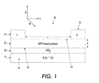
- FIGURE 1 illustrates an exemplary configuration of an OTFT 10 which may be formulated with the exemplary DPP-based compounds.
- the OTFT 10 comprises a substrate 12, gate, source, and drain electrodes 14, 16, and 18, respectively, a dielectric layer 20, and a semiconductor layer 22, which may be formed in accordance with exemplary embodiments disclosed herein.
- Substrate 12 comprises or is in contact with gate electrode 14.
- the gate electrode 14 is depicted as being wholly within the substrate 12 (the entire substrate serves as the gate electrode in this embodiment), this is not required; the key is that the dielectric layer 20 separates the gate electrode 14 from the source electrode 16, drain electrode 18, and the semiconductor layer 22.
- gate electrode 14 may be formed as a channel in substrate 12, e.g., by doping a portion of the substrate, or may be formed as a surface layer on the substrate 12.
- the illustrated semiconductor layer 22 has opposed first and second planar surfaces 24, 26.
- the source electrode 16 contacts the semiconductor layer 22.
- the drain electrode 18 also contacts the same surface 24 of the semiconductor layer 22.
- the semiconductor layer 22 runs over the dielectric layer 20 and extends between the source and drain electrodes 16 and 18.
- the OTFT device includes a semiconductor channel with a width W and length L (perpendicular to the page in FIG. 1 ).
- the substrate 12 may be formed e.g., of a heavily n-doped silicon wafer.
- the substrate 12 may be composed of silicon, glass plate, plastic film or sheet or other suitable substrate material.
- a plastic substrate such as for example polyester, polycarbonate, polyimide sheets and the like may be employed.
- the thickness of the substrate 12 may be from about 10 micrometers to over 10 millimeters with a representative thickness being from about 50 to about 100 micrometers, especially for a flexible plastic substrate and from about 1 to about 10 millimeters for a rigid substrate, such as glass plate or silicon wafer.
- the semiconductor layer 22 has a thickness H ranging for example from about 10 nanometers to about 1 micrometer, e.g., from about 20 to about 200 nanometers.
- the semiconductor channel width W may be, for example, from about 1 micrometers to about 5 millimeters, with a specific channel width being about 5 micrometers to about 1 millimeter.
- the semiconductor channel length L may be, for example, from about 1 micrometer to about 1 millimeter with a more specific channel length being from about 5 micrometers to about 100 micrometers.
- the gate, source, drain and electrodes 14, 16, 18 can be made of any suitable electrically conductive materials.
- the gate electrode 14 can be, for example, a thin metal film, a conducting polymer film, a conducting film made from conducting ink or paste or the substrate itself, for example heavily doped silicon.
- Examples of gate electrode materials include but are not restricted to aluminum, gold, silver, chromium, indium tin oxide, conducting polymers such as polystyrene sulfonate-doped poly(3,4-ethylenedioxythiophene) (PSS-PEDOT), conducting ink/paste comprised of carbon black/graphite or colloidal silver dispersion in polymer binders, such as ELECTRODAGTM available from Acheson Colloids Company.
- the gate electrode layer can be prepared by vacuum evaporation, sputtering of metals or conductive metal oxides, coating from conducting polymer solutions or conducting inks by spin coating, casting or printing, or doping of the substrate.
- the illustrated gate electrode 14 is formed from n-doped silicon.
- the thickness of the gate electrode layer ranges for example from about 10 to about 200 nanometers for metal films and in the range of about 1 to about 10 micrometers for polymer conductors.
- Typical materials suitable for use as source and drain electrodes 16, 18 include those of the gate electrode materials such as gold, nickel, aluminum, platinum, conducting polymers and conducting inks.
- the source and drain electrodes 16, 18 are formed from an electrically conductive material, such as gold.
- Typical thicknesses of source and drain electrodes are about, for example, from about 40 nanometers to about 1 micrometer with the more specific thickness being about 100 to about 400 nanometers.
- the dielectric layer 20 generally can be an inorganic material film or an organic polymer film.
- inorganic materials suitable as the gate dielectric layer include silicon oxide, silicon nitride, aluminum oxide, barium titanate, barium zirconium titanate and the like;
- organic polymers for the gate dielectric layer include polyesters, polycarbonates, poly(vinyl phenol), polyimides, polystyrene, poly(methacrylate)s, poly(acrylate)s, epoxy resin and the like.
- a thermally grown silicon oxide (SiO 2 ) may be used as the dielectric layer 20.
- the thickness of the dielectric layer 20 is, for example from about 10 nanometers to about 2000 nanometers depending on the dielectric constant of the dielectric material used.
- a representative thickness of the dielectric layer is from about 100 nanometers to about 500 nanometers.
- the dielectric layer may have a conductivity that is for example less than about 10 -12 S/cm.
- the gate dielectric layer, the gate electrode, the semiconductor layer, the source electrode, and the drain electrode are formed in any sequence with the gate electrode and the semiconductor layer both contacting the dielectric layer, and the source electrode and the drain electrode both contacting the semiconductor layer.
- the phrase "in any sequence" includes sequential and simultaneous formation.
- the source electrode and the drain electrode can be formed simultaneously or sequentially.
- the source electrode is grounded and a bias voltage of generally, for example, about 0 volt to about -80 volts is applied to the drain electrode to collect the charge carriers transported across the semiconductor channel when a voltage of generally about +20 volts to about -80 volts is applied to the gate electrode.
- the semiconductor layer 22 incorporating the present polymer in an OTFT device generally exhibits a field-effect mobility of greater than for example about 10 -3 cm 2 /Vs (square centimeter per Volt per second), and an on/off ratio of greater than for example about 10 3 .
- On/off ratio refers to the ratio of the source-drain current when the transistor is on to the source-drain current when the transistor is off.
- the field-effect mobility is greater than about 10 -2 cm 2 /Vs and in some embodiments, is greater than about 5 x 10 -2 cm 2 /Vs, e.g., 0.08 - 0.12 cm 2 /Vs.
- the on/off ratio is at least 10 4 and in some embodiments, 10 5 or higher, e.g., about 10 6 .
- the exemplary semiconductor layer 22 comprises a compound (small molecule, oligomer, or polymer) comprising a pyrrolo[3,4-c]pyrrole-1,4-dione moiety (DPP moiety or unit):
- each R is independently selected from: hydrogen, a hydrocarbon, such as alkyl or aryl, and a hetero-containing group, such as heteroaryl.
- the DPP moiety is substituted with two Ar groups, where each Ar is independently aryl or heteroaryl and where each Ar may be a terminal group or not a terminal group. Unless otherwise noted, all alkyl, aryl, and heteroaryl groups disclosed herein may be substituted or unsubstituted.
- structure (IV) is representative of all three structures, since a and n can independently be 1 and b can be 0.
- Exemplary conjugated moieties M include, but are not limited to the following, and optionally substituted derivatives thereof: wherein each R' is independently selected from: hydrogen, a hydrocarbon such as alkyl or aryl, a hetero-containing group such as heteroaryl or alkoxy, and halogen. Any of the above exemplary conjugated moieties M can be substituted, for example, by replacement of one or more of the hydrogens with an alkyl, aryl, alkylaryl, halogen, or hydroxyl group, combination thereof, or the like.
- exemplary hydrocarbons may include any suitable optionally substituted hydrocarbon group.
- the optionally substituted hydrocarbon group contains for example from 1 to about 50 carbon atoms, or from 4 to about 20 carbon atoms, and may be selected from, for example, a straight chain alkyl group, a branched alkyl group, a cycloalkyl group, an aryl group, an alkylaryl group, and an arylalkyl group.
- alkyl groups suitable for R include, but are not limited to methyl, ethyl, propyl, butyl, pentyl, hexyl, heptyl, octyl, nonyl, decyl, undecyl, dodecyl, tridecyl, tetradecyl, pentadecyl, hexadecyl, heptadecyl, octadecyl, cyclopentyl, cyclohexyl, cycloheptyl, and isomers thereof.
- the alkyl group is optionally substituted one or more times with, for example, a halogen (chlorine, bromine, fluorine, and iodine) or a heteroatom-containing group as described herein, or a mixture thereof.
- aryl groups are aromatic hydrocarbon groups (including alkoxyaryl and alkylaryl groups) having 6 to 500 carbon atoms, and which are suitable for R include, but are not limited to phenyl, polyphenyl, and naphthyl; alkoxyphenyl groups, such as p-methoxyphenyl, m-methoxyphenyl, o-methoxyphenyl, ethoxyphenyl, p-tert-butoxyphenyl, and m-tert-butoxyphenyl; alkylphenyl groups such as 2-methylphenyl, 3-methylphenyl, 4-methylphenyl, ethylphenyl, 4-tert-butylphenyl, 4-butylphenyl, and dimethylphenyl; alkylnaphthyl groups such as methylnaphthyl and ethylnaphthyl; alkoxynaphthyl groups such as methoxynaph
- heteroatom-containing groups suitable for R or as substituents for alkyl groups used as R may include any suitable heteroatom and may include, but are not limited to, a nitrogen containing moiety, an alkoxy group, a heterocyclic system, an alkoxyaryl, and an arylalkoxy.
- Representative heteroatom-containing groups include for example cyano, nitro, methoxyl, ethoxyl, and propoxyl as the heteroatom.
- the heteroatom containing group has for example 2 to about 120 atoms, or from 2 to about 80 atoms.
- exemplary hydrocarbons and hetero-containing groups include those listed for R above.
- R' being halogen
- any suitable halogen can be used (chlorine, bromine, fluorine, or iodine).
- heteroaryl groups include those heteroaryl groups suggested for R.
- Heteroaryl groups are heterocycles which include an unsaturated ring comprising at least two carbon atoms (generally, at least four carbon atoms) and at least one atom which is a different atom from carbon (a heteroatom, such as S, Se, O, or N).
- the heteroaryl group may have, for example, 5 to about 120 atoms, or from 10 to about 80 atoms.
- the heteroaryl group is an electron-donating group, which assists in the hole transport.
- each of these exemplary heteroatoms includes a lone electron pair, which helps the hole transport.
- exemplary heteroaryl groups include those heteroaryl groups suggested for R.
- Ar is an optionally substituted heteroaryl group which includes one or more repeat units of a five-membered ring, such as thiophene, furan, or pyrrole.
- heteroaryl groups are also contemplated for Ar, such as oxazole, isoxazole, pyridine, thiazole, isothiazole, imidazole, triazole, pyrazole, furazan, thiadiazole, oxadiazole, pyridazine, pyrimidine, pyrazine, indole, isoindole, indazole, chromene, quinoline, isoquinoline, cinnoline, quinazoline, quinoxaline, naphthylidine, phthalazine, purine, pteridine, thienofuran, imidazothiazole, benzofuran, benzothiophene, benzoxazole, benzthiazole, benzthiadiazole, benzimidazole, imidazopyridine, pyrrolopyridine, pyrrolopyrimidine, pyridopyrimidine, and combinations thereof.
- the heteroaryl group includes a five-membered unsaturated ring comprising a single heteroatom, such as S, Se, O, or N in the form of NR", where R" is as defined for R in structures (I)-(IV) above, and is bonded to the respective fused ring of the DPP moiety by this five-membered unsaturated ring.
- Structure (V) illustrates an exemplary polymer according to structure (IV) in which Ar comprises an optionally substituted five-membered heterocycle, that is suited to use in the exemplary semiconductor layer:
- each X is independently a heteroatom, for example, S, Se, O, or NR
- each R is as previously defined and each R" is as defined for R in structures (I)-(IV) above.
- R or R" is hydrogen, an optionally substituted hydrocarbon such as alkyl or aryl, or a hetero-containing group such as heteroaryl
- each Z is independently an optionally substituted hydrocarbon such as alkyl or aryl, a hetero-containing group such as CN, a heteroaryl, or a halogen, such as Br, Cl, or F
- d represents a number which is at least 1, e.g., from 1 to about 10
- e represents the number of Z, and can be from zero to 2
- R, M, a, b, and n may be as previously defined for structures (II)-(IV).
- d, q, and b may be the same or approximately the same for each repeat unit so that the copolymer has a regular structure.
- Z is an optionally substituted hydrocarbon or heteroaryl, it can be as previously defined for R.
- e is zero and the structure V can be represented by structure VI:
- each Ar group represented by: includes at least one heterocycle such as thiophene, furan, or pyrrole.
- the layer includes a compound which includes a structure (VII): where X, R, Z, d, e, and n are as defined for structure (V) above.
- n is from 2 to 5000.
- n is from 10-50.
- R is an alkyl group having from 1 to 50 carbon atoms.
- e is zero and the structure is represented by structure VIII:
- Exemplary compounds according to formula (VIII) for forming a semiconducting layer include those which include a poly(2,5-dialkyl/diaryl-3,6-bis(thienyl/furyl/pyrrolyl-5-yl)-diketopyrrolopyrrole).
- d has the same or approximately the same value for each repeat unit, so that the backbone is a regular polymer.
- Exemplary semiconducting compounds in accordance with the exemplary embodiment include: and mixtures thereof, wherein n is the number of repeat units and can be from about 2 to about 5000, R''', R''', and R''' can be the same or different substituent, and wherein the substituent is independently selected from the group consisting of an optionally substituted hydrocarbon group and a heteroatom-containing group,
- Y is a halogen atom selected from F, Cl, and Br.
- structures (10), (11), (12), (13), (22), (23), (24), (25), (34), (35), (36), (37), (44), (45), (46), (47), (48), (49), (50), and (51) represent exemplary heteroaryl di-substituted DPP-based polymers in accordance with one aspect of the exemplary embodiment.
- a polymer formed according to structure (VI) a polymer based on poly(2,5-dialkyl-3,6-bis(thienyl-5-yl)-diketopyrrolopyrrole) may be used, for example, in a semiconductor layer.
- Such a polymer may thus have the general formula: wherein n is a number of repeat units and can be from 2 to about 5000 and each R''' is an alkyl, independently selected from the group consisting of butyl, pentyl, hexyl, heptyl, octyl, nonyl, decyl, undecyl, dodecyl, tridecyl, tetradecyl, pentadecyl, hexadecyl, heptadecyl, octadecyl, nonadecynyl, and eicosanyl.
- An example is poly(2,5-dioctadecyl-3,6-bis(thienyl-5-yl)-diketopyrrolopyrrole).
- the electron-withdrawing nature of the diketone and the high coplanarity of this structure give these polymers high field-effect mobility and excellent air-stability when the polymers are used as p-channel semiconductors in OTFTs.
- the five-membered heterocycles, such as thiophene, furan, and pyrrole, in the polymers are electron-rich and thus facilitate hole injection and transport in the TFT devices.
- the less steric effect of the five-membered heterocycles minimizes the twisting of the polymer backbone, leading to high coplanarity of the backbone, a feature for achieving high mobility.
- the layer may comprise a small molecule, oligomer, or polymer based on any of structures (II) to (VI), or combination thereof.
- the polymer may include one or more types of repeat units of which the stucture (II) to (VI) serves as at least one repeat unit.
- the layer 22 may be formed exclusively of the small molecule, oligomer, or polymer(s) or may comprise additional componds, such as binders, solvents, dopants, and the like.
- the layer comprises at least 1 volume percent of the compound according to any of the structures disclosed herein. In another embodiment, the layer comprises at least 10 volume percent or at least 50 volume percent of the compound and can comprise up to 100% of the compound.
- the exemplary compound may be dispersed in the binder for assisting the deposition of the layer 22 during formation of a semiconductor device and/or the binder may serve as a matrix for retaining the compound in the layer 22.
- a layer may be formed which includes polystyrene as a binder in addition to one or more of the exemplary compounds.
- the binder may comprise from 0.1-99 vol. % of the layer 22, e.g., less than 50 vol.% of layer 22.
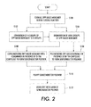
- the polymer of any one of structures (V) (VI), (VII), and (VIII) may be prepared by a four step process, as illustrated in FIGURE 2 .
- a DPP moiety may be formed by reacting 2 moles of an appropriate nitrile or a Schiff base with one mole of a succinic acid diester in the presence of a base and an organic solvent.
- a carbonitrile (Ar-CN) for forming the selected Ar group e.g., thiophenecarbonitrile
- Ar-CN carbonitrile
- diisopropyl succinate under suitable conditions for ring closure of the DPP moiety to form a monomer M1 of the general formula: where Ar is e.g., and where Z, e, X, and b are as defined above.
- step S100 may be carried out in solution in the presence of a sodium alkoxide, such as t-C 5 H 11 ONa, which may be formed in situ, followed by neutralization with an organic acid, such as galcial acetic acid.
- a sodium alkoxide such as t-C 5 H 11 ONa
- the reaction may be performed at a suitable reaction temperature, such as about 85°C.
- U.S. Patent No. 4,579,949 provides further details of reactions for forming DPP molecules.
- the H groups on the monomer (M1) obtained at step S100 may optionally be converted from H to a selected R group by reaction of the monomer with a halide of the formula R-Y, where R is as defined above (other than H) and Y is a halogen which may be selected from chlorine, bromine, and iodine.
- R-Y a halogen which may be selected from chlorine, bromine, and iodine.
- Step S102 may be performed in solution at a suitable reaction temperature, such as about 40 to 180°C (e.g., about 120°C).
- the reaction may be carried out in a suitable solvent, such as dimethylformamide, in the presence of an aqueous base, such as an alkali metal hydroxide or carbonate and a crown ether, such as 18-crown-6.
- aqueous bases include NaOH, KOH, Na 2 CO 3 , K 2 CO 3 and the like, e.g., an aqueous K 2 CO 3 solution.
- the molar ratio of the base to compound M1 is chosen in the range of from 0.5:1 to 50:1.
- the Ar groups are halogenated, for example, by reaction of the monomer (M1) or (M2) formed in step S100 or S102 with a halogen, such as bromine, chlorine, or iodine, to form a monomer of the general formula:
- Y can be a halogen, such as bromine, chlorine, or iodine.
- Step S104 may be carried out in any suitable non-reactive medium, such as chloroform, e.g., at room temperature or above.
- the monomer (M3) is polymerized to form a homopolymer of the general structure (III) above.
- Ar is the resulting polymer has the structure (VIII) above.
- the monomer (M3) may be copolymerized with a comonomer for forming units M of structure (IV) (V), or (VI), as defined above.
- Suitable comonomers for providing the M unit include thiophene, furan, pyrrole, thieno[3,2-b]thiophene, benzo[1,2-b:4,5-b']dithiophene, and combinations thereof.
- Step S106 or S108 may be performed in solution in the presence of a ditin compound, such as an hexaalkylditin or hexaarylditin compound such as hexamethylditin, hexa-n-butylditin, or hexaphenylditin, and a catalyst suitable for coupling reactions or for polycondensation reactions, optionally in the presence of copper(I) iodide.
- a ditin compound such as an hexaalkylditin or hexaarylditin compound such as hexamethylditin, hexa-n-butylditin, or hexaphenylditin
- a catalyst suitable for coupling reactions or for polycondensation reactions optionally in the presence of copper(I) iodide.
- a suitable coupling catalyst is a palladium-based catalyst, e.g., a tetrakis(triarylphosphonium)-palladium catalyst, such as tetrakis(triphenylphosphine)palladium(0) (Pd(PPh 3 ) 4 ), or derivatives thereof.
- the catalyst is added in a molar ratio of DPP monomer to the catalyst in the range of from about 1000:1 to about 10:1, e.g., from about 100:1 to about 30:1.
- a suitable solvent for the reaction may be a mixture of THF and 1-methyl-2-pyrrolidinone (NMP). The reaction may be carried out under reflux at a temperature which is at or slightly above the boiling point of the solvent.
- the resulting polymer may be purified, e.g., by Soxhlet extraction.
- the polymers/copolymers thus formed may have a weight average molecular weight M w in the range of from 700 to 1,000,000, e.g., at least about 5000.
- a layer comprising the polymer may be incorporated into a semiconductor device.
- the resulting polymer (III), (IV), (V), (VI), (VII), or (VIII) may be dissolved in a suitable solvent, such as dichlorobenzene, and the solution deposited on a dielectric layer, for example, by spin coating, casting, vacuum deposition, or the like.
- the dielectric layer may be a silicon oxide layer which has been grown on a doped silicon wafer.
- the deposition of the semiconductor polymer may be performed under ambient conditions, e.g., in air or other atmosphere in which oxygen may be present in significant amounts, e.g., in an atmosphere where oxygen is above about 5% by weight, and at a temperature of about 25°C.
- the deposition may also be performed without excluding moisture in the atmosphere. For example, the deposition may be performed at a relative humidity of about 10%, or higher.
- a thin layer (e.g., less than 5 nanometers thick, such as a monolayer) of an organosilane, may be provided on the dielectric layer by modifying the dielectric layer with a reactive organosilane, such as octyltrichlorosilane, prior to deposition of the semiconductor polymer layer.
- a reactive organosilane such as octyltrichlorosilane
- the resulting semiconductor layer may be then dried, for example, in a vacuum oven at 80 °C for 5-10 hours. Subsequently, source and drain electrodes may be patterned on the semiconductor layer, e.g., by gold deposition on top of the semiconductor layer by vacuum deposition through a shadow mask.
- the resulting semiconductor device may be annealed at a suitable temperature, such as about 140 °C for 10-15 min, without risking damage to the semiconductor polymer.
- the following Examples provide a reaction scheme for forming one exemplary polymer according to structure (VIII) and an OTFT formed therefom.
- reaction mixture was then cooled to 50 °C, diluted with 50 mL of methanol, and then slowly neutralized with ⁇ 15 mL of glacial acetic acid and refluxed briefly, and the reaction mixture was filtered. After the residue was washed several times with hot methanol and water, the resultant solid was dried in vacuo at 50 °C. A bluish-red solid (11 g, yield 92%) was obtained (compound (1)).
- a top-contact thin film transistor configuration as schematically illustrated in FIGURE 1 was selected as a test device structure.
- the test device was built on an n-doped silicon wafer with a thermally grown silicon oxide layer 20 with a thickness of about 200 nanometers thereon, and had a capacitance of about 15 nF/cm 2 (nanofarads/square centimeter), as measured with a capacitor meter.
- the wafer functioned as the gate electrode while the silicon oxide layer acted as the gate dielectric.
- n-doped silicon wafer with silicon oxide layer thereon was first cleaned with isopropanol, argon plasma, isopropanol and air dried, and then immersed in a 0.1 M solution of octyltrichlorosilane (OTS-8) in toluene at 60 °C for 20 min. Subsequently, the wafer was washed with toluene, isopropanol and air-dried.
- OTS-8 octyltrichlorosilane
- a solution of polymer (4) (poly(2,5-dioctadecyl-3,6-bis(thienyl-5-yl)-diketopyrrolopyrrole)) dissolved in dichlorobenzene (0.5 percent by weight) was first filtered through a 1.0 micrometer syringe filter, and then spin-coated on the OTS-8-treated silicon wafer at 1000 rpm for 120 seconds at room temperature. This resulted in the formation of a semiconductor layer with a thickness of 20-50 nanometers on the silicon wafer, which was then dried in a vacuum oven at 80°C for 5-10 hr.
- gold source and drain electrodes of about 50 nanometers in thickness were deposited on top of the semiconductor layer by vacuum deposition through a shadow mask with various channel lengths and widths, thus creating a series of transistors of various dimensions.
- the devices were annealed at 140°C for 10-15 min before evaluation.
- the evaluation of transistor performance was accomplished in a black box (that is, a closed box which excluded ambient light) at ambient conditions using a Keithley 4200 SCS semiconductor characterization system.
- the mobility and current on-to-off ratio are comparable to polythiophenes (e.g., poly(3-hexylthiophene) (P3HT) and poly[thiophene] (PQT)).
- P3HT poly(3-hexylthiophene)
- PQT poly[thiophene]
- the OTFT devices were fabricated and measured entirely under ambient conditions, indicating the excellent air-stability of this type of polymers.
Landscapes
- Chemical & Material Sciences (AREA)
- Health & Medical Sciences (AREA)
- Chemical Kinetics & Catalysis (AREA)
- Medicinal Chemistry (AREA)
- Polymers & Plastics (AREA)
- Organic Chemistry (AREA)
- Engineering & Computer Science (AREA)
- Materials Engineering (AREA)
- Thin Film Transistor (AREA)
- Polyoxymethylene Polymers And Polymers With Carbon-To-Carbon Bonds (AREA)
- Electroluminescent Light Sources (AREA)
Applications Claiming Priority (1)
| Application Number | Priority Date | Filing Date | Title |
|---|---|---|---|
| US11/850,965 US7932344B2 (en) | 2007-09-06 | 2007-09-06 | Diketopyrrolopyrrole-based polymers |
Publications (2)
| Publication Number | Publication Date |
|---|---|
| EP2033983A2 true EP2033983A2 (fr) | 2009-03-11 |
| EP2033983A3 EP2033983A3 (fr) | 2009-11-25 |
Family
ID=40202913
Family Applications (1)
| Application Number | Title | Priority Date | Filing Date |
|---|---|---|---|
| EP08160873A Withdrawn EP2033983A3 (fr) | 2007-09-06 | 2008-07-22 | Polymères à base de Diketopyrrolopyrrole |
Country Status (4)
| Country | Link |
|---|---|
| US (1) | US7932344B2 (fr) |
| EP (1) | EP2033983A3 (fr) |
| JP (1) | JP5311936B2 (fr) |
| TW (1) | TWI402292B (fr) |
Cited By (17)
| Publication number | Priority date | Publication date | Assignee | Title |
|---|---|---|---|---|
| WO2010136352A1 (fr) * | 2009-05-27 | 2010-12-02 | Basf Se | Procédé de polymérisation de composés (hétéro)aromatiques |
| WO2011119446A1 (fr) * | 2010-03-20 | 2011-09-29 | Polyera Corporation | Composés semi-conducteurs à pyrrolo[3,2-b]pyrrole et dispositifs qui incorporent lesdits composés |
| CN102372842A (zh) * | 2010-08-19 | 2012-03-14 | 海洋王照明科技股份有限公司 | 含噻吩吡咯二酮单元的共聚物及其制备方法和应用 |
| WO2012175530A1 (fr) | 2011-06-22 | 2012-12-27 | Basf Se | Oligomères de dicétopyrrolopyrrole destinés à être utilisés dans des dispositifs semi-conducteurs organiques |
| WO2013030325A1 (fr) | 2011-09-02 | 2013-03-07 | Basf Se | Oligomères de dicétopyrrolopyrrole et compositions comprenant des oligomères de dicétopyrrolopyrrole |
| CN103012751A (zh) * | 2012-11-30 | 2013-04-03 | 四川大学 | 一类双噻吩基吡咯并[3,4-c]吡咯-1,4-二酮与(杂)芳烃共聚物的制备方法 |
| WO2013028441A3 (fr) * | 2011-08-19 | 2013-06-06 | University Of Washington | Nouveaux poly(hétéroarylène-vinylène)s à base de dicétopyrrolopyrrole |
| US8624232B2 (en) | 2009-08-28 | 2014-01-07 | Prashant Sonar | Ambipolar polymeric semiconductor materials and organic electronic devices |
| US8765968B2 (en) | 2009-08-28 | 2014-07-01 | Agency For Science, Technology And Research | Polymeric semiconductors, devices, and related methods |
| US8796469B2 (en) | 2009-03-23 | 2014-08-05 | Basf Se | Diketopyrrolopyrrole polymers for use in organic semiconductor devices |
| US8912305B2 (en) | 2008-10-31 | 2014-12-16 | Basf Se | Diketopyrrolopyrrole polymers for use in organic field effect transistors |
| CN104211920A (zh) * | 2013-05-29 | 2014-12-17 | 海洋王照明科技股份有限公司 | 共轭聚合物及其制备方法与应用 |
| US8975359B2 (en) | 2008-10-31 | 2015-03-10 | Basf Se | Diketopyrrolopyrrole polymers for use in organic semiconductor devices |
| CN106750193A (zh) * | 2016-12-12 | 2017-05-31 | 中国科学院化学研究所 | 连三吡咯并吡咯二酮聚合物及其合成方法与应用 |
| EP2571919B1 (fr) * | 2010-05-19 | 2018-07-11 | Basf Se | Polymères de dicétopyrrolopyrrole destinés à être utilisés dans des dispositifs à semi-conducteur organique |
| US10224484B2 (en) | 2008-10-31 | 2019-03-05 | Basf Se | Diketopyrrolopyrrole polymers for use in organic field effect transistors |
| US10424737B2 (en) | 2006-06-30 | 2019-09-24 | Basf Se | Diketopyrrolopyrrole polymers as organic semiconductors |
Families Citing this family (39)
| Publication number | Priority date | Publication date | Assignee | Title |
|---|---|---|---|---|
| JP5431340B2 (ja) * | 2007-10-09 | 2014-03-05 | ビーエーエスエフ ソシエタス・ヨーロピア | ピロロピロール誘導体、その製造及び使用 |
| CN102113138A (zh) * | 2008-08-01 | 2011-06-29 | 欧瑞康太阳Ip股份公司(特吕巴赫) | 用于制作光伏电池结构的方法 |
| JP5396128B2 (ja) * | 2009-03-31 | 2014-01-22 | 大阪瓦斯株式会社 | ジケトピロロピロール骨格を有するポリマーおよび白色発光材料 |
| TWI602844B (zh) * | 2010-05-19 | 2017-10-21 | 巴地斯顏料化工廠 | 用於有機半導體裝置之二酮基吡咯并吡咯聚合物 |
| CN102276804B (zh) * | 2010-06-13 | 2013-04-17 | 海洋王照明科技股份有限公司 | 含双噻吩并吡咯单元苝四羧酸二酰亚胺共聚物及其制备方法和应用 |
| WO2012032949A1 (fr) * | 2010-09-10 | 2012-03-15 | 住友化学株式会社 | Composé polymère et transducteur photoélectrique organique |
| US8946376B2 (en) * | 2010-09-29 | 2015-02-03 | Basf Se | Semiconductors based on diketopyrrolopyrroles |
| WO2012050070A1 (fr) * | 2010-10-13 | 2012-04-19 | 住友化学株式会社 | Composé de masse moléculaire élevée et élément de conversion photoélectrique organique l'utilisant |
| WO2012060283A1 (fr) * | 2010-11-02 | 2012-05-10 | 住友化学株式会社 | Composé macromoléculaire et élément de conversion photoélectrique organique l'utilisant |
| US8598450B2 (en) | 2010-11-24 | 2013-12-03 | Polyera Corporation | Conjugated polymers and their use in optoelectronic devices |
| US8158744B1 (en) | 2011-03-01 | 2012-04-17 | Xerox Corporation | Dithioketopyrrolopyrrole-based polymers |
| CN103597601B (zh) * | 2011-03-29 | 2016-09-21 | 加利福尼亚大学董事会 | 用于电光器件的活性材料和电光器件 |
| EP2696660A4 (fr) * | 2011-04-06 | 2014-10-22 | Konica Minolta Inc | Procédé de fabrication d'élément électroluminescent organique et élément électroluminescent organique |
| WO2012165128A1 (fr) * | 2011-05-27 | 2012-12-06 | 住友化学株式会社 | Composé de masse moléculaire élevée et élément organique de conversion photoélectrique |
| EP2565504A1 (fr) * | 2011-09-02 | 2013-03-06 | Aurotec GmbH | Pièce de raccordement d'une conduite de transport |
| US8846855B2 (en) | 2011-10-31 | 2014-09-30 | Corning Incorporated | Conjugated fused thiophenes, methods of making conjugated fused thiophenes, and uses thereof |
| KR101286014B1 (ko) * | 2011-11-21 | 2013-07-18 | 광주과학기술원 | 팔라듐계 촉매를 사용한 직접적 ch 아릴화 방법 |
| US8901544B2 (en) | 2011-12-06 | 2014-12-02 | Corning Incorporated | Organic thin film transistor with ion exchanged glass substrate |
| US8598299B2 (en) | 2011-12-06 | 2013-12-03 | Xerox Corporation | Semiconductor composition |
| KR101990167B1 (ko) * | 2011-12-07 | 2019-06-17 | 바스프 에스이 | 유기 전계 효과 트랜지스터 |
| US8558109B2 (en) | 2012-03-19 | 2013-10-15 | Xerox Corporation | Semiconductor composition for high performance organic devices |
| US8563851B2 (en) | 2012-03-19 | 2013-10-22 | Xerox Corporation | Method to increase field effect mobility of donor-acceptor semiconductors |
| US9379335B2 (en) | 2012-04-08 | 2016-06-28 | The Regents Of The University Of California | Benzodipyrrolidones and their polymers: synthesis and applications for organic electronics and optoelectronics |
| JP2013254818A (ja) * | 2012-06-06 | 2013-12-19 | Hiroshima Univ | 有機半導体材料及び有機半導体材料用中間体 |
| US9214258B2 (en) * | 2012-12-06 | 2015-12-15 | Xerox Corporation | Semiconductor composites comprising carbon nanotubes and diketopyrrolopyrrole-thiophene based copolymers |
| US8865861B2 (en) | 2012-12-27 | 2014-10-21 | Xerox Corporation | Pechmann dye based polymers and semiconductor compositions |
| US8575477B1 (en) * | 2012-12-27 | 2013-11-05 | Xerox Corporation | Diketopyrrolopyrrole-based polymers containing a diene group for semiconductors |
| US8809484B2 (en) | 2012-12-27 | 2014-08-19 | Xerox Corporation | Extended isoindigo polymers and semiconductor compositions |
| KR101443295B1 (ko) * | 2013-02-25 | 2014-09-22 | 국립대학법인 울산과학기술대학교 산학협력단 | 주극성 변환이 가능한 신규한 양극성 유기 반도체 화합물과 이를 포함하는 유기 박막트랜지스터 |
| US9761803B2 (en) | 2013-07-22 | 2017-09-12 | Xerox Corporation | Semiconductor composition |
| CN105637009B (zh) * | 2013-09-16 | 2018-06-12 | 株式会社Lg化学 | 共聚物和包含其的有机太阳能电池 |
| US10381583B2 (en) | 2013-12-05 | 2019-08-13 | Xerox Corporation | Electronic device |
| WO2015108360A1 (fr) * | 2014-01-17 | 2015-07-23 | 경상대학교산학협력단 | Polymère de dicétopyrrolopyrrole asymétrique contenant un hétérocycle-vinylène-hétérocyclique, dispositif électronique organique l'utilisant, et monomère pour le préparer |
| US9399698B2 (en) | 2014-01-31 | 2016-07-26 | Xerox Corporation | Processes for purifying diketopyrrolopyrrole copolymers |
| KR101600031B1 (ko) * | 2014-03-24 | 2016-03-07 | 경상대학교산학협력단 | 비대칭 다이케토피롤로피롤 중합체 및 이를 함유하는 유기 전자 소자 |
| US9580556B2 (en) | 2015-01-29 | 2017-02-28 | Corning Incorporated | DPP with branched alkyl-chain or (and) fused thiophene with branched alkyl-chain and the related designing strategy to increase the molecular weight of their semi-conducting copolymers |
| US10109798B2 (en) * | 2015-05-26 | 2018-10-23 | Purdue Research Foundation | Methods and compositions for enhancing processability and charge transport of polymer semiconductors |
| WO2017086320A1 (fr) * | 2015-11-20 | 2017-05-26 | 富士フイルム株式会社 | Composition de semi-conducteur organique, film semi-conducteur organique, transistor à couches minces organique et procédé permettant de fabriquer un transistor à couches minces organique |
| US10050203B2 (en) | 2016-05-27 | 2018-08-14 | Samsung Electronics Co., Ltd. | Polymer and electronic device and organic thin film transistor including the same |
Citations (4)
| Publication number | Priority date | Publication date | Assignee | Title |
|---|---|---|---|---|
| US4579949A (en) | 1982-05-17 | 1986-04-01 | Ciba-Geigy Corporation | Preparation of pyrrolo[3,4-c]pyrroles |
| US6107117A (en) | 1996-12-20 | 2000-08-22 | Lucent Technologies Inc. | Method of making an organic thin film transistor |
| US20070112171A1 (en) | 2005-11-16 | 2007-05-17 | Xerox Corporation | Polymer having thieno[3,2-b] thiophene moieties statement regarding federally sponsored research or development |
| US20070160847A1 (en) | 2005-12-21 | 2007-07-12 | Xerox Corporation | Organic thin-film transistors |
Family Cites Families (18)
| Publication number | Priority date | Publication date | Assignee | Title |
|---|---|---|---|---|
| EP0061426B1 (fr) * | 1981-03-20 | 1985-02-13 | Ciba-Geigy Ag | Procédé de coloration des matières organiques à poids moléculaire élevés et des pigments polycycliques |
| DE59707889D1 (de) * | 1996-01-30 | 2002-09-12 | Ciba Sc Holding Ag | Polymerisierbare Diketopyrrolopyrrole und damit hergestellte Polymere |
| TWI290164B (en) * | 1999-08-26 | 2007-11-21 | Ciba Sc Holding Ag | DPP-containing conjugated polymers and electroluminescent devices |
| US20020060321A1 (en) * | 2000-07-14 | 2002-05-23 | Kazlas Peter T. | Minimally- patterned, thin-film semiconductor devices for display applications |
| DE60235679D1 (de) * | 2001-08-17 | 2010-04-29 | Merck Patent Gmbh | Konjugierte Copolymere aus Dithienothiophen und Vinylen oder Acetylen |
| CA2469269A1 (fr) * | 2002-02-01 | 2003-08-07 | Ciba Specialty Chemicals Holding Inc. | Compositions fluorescentes comprenant des dicetopyrrolopyrroles |
| DE602004021211D1 (de) * | 2003-03-07 | 2009-07-09 | Merck Patent Gmbh | Fluorene und Arylgruppen enthaltende Mono-, Oligo- und Polymere |
| DE602004017550D1 (de) | 2003-08-28 | 2008-12-18 | Merck Patent Gmbh | Mono-, Oligo- und Polythienoi2,3-b thiophene |
| DE602004024629D1 (de) * | 2003-10-15 | 2010-01-28 | Merck Patent Gmbh | Polybenzodithiophene |
| CN101747493B (zh) | 2003-10-28 | 2014-07-02 | 西巴特殊化学品控股有限公司 | 二酮基吡咯并吡咯聚合物 |
| DE602005017384D1 (de) * | 2004-05-18 | 2009-12-10 | Merck Patent Gmbh | Mono-, oligo- und polythienoä3,2-büthiophene |
| ATE550340T1 (de) * | 2004-08-21 | 2012-04-15 | Merck Patent Gmbh | Polymere von thienoä2,3-büthiophen |
| US7170093B2 (en) * | 2004-11-05 | 2007-01-30 | Xerox Corporation | Dielectric materials for electronic devices |
| JP2006232898A (ja) * | 2005-02-23 | 2006-09-07 | Ricoh Co Ltd | 導電性高分子材料、それを用いた電界効果型トランジスタ及びその製造方法 |
| JP2007067263A (ja) * | 2005-09-01 | 2007-03-15 | Konica Minolta Holdings Inc | 有機半導体材料、有機半導体膜、有機半導体デバイス及び有機薄膜トランジスタ |
| US7632703B2 (en) * | 2005-12-22 | 2009-12-15 | Xerox Corporation | Organic thin-film transistors |
| JP5229520B2 (ja) * | 2006-03-14 | 2013-07-03 | 株式会社リコー | 新規なベンゾジチオフェン重合体 |
| US20090302311A1 (en) | 2006-06-30 | 2009-12-10 | Turbiez Mathieu G R | Diketopyrrolopyrrole polymers as organic semiconductors |
-
2007
- 2007-09-06 US US11/850,965 patent/US7932344B2/en active Active
-
2008
- 2008-07-22 EP EP08160873A patent/EP2033983A3/fr not_active Withdrawn
- 2008-09-04 TW TW097133848A patent/TWI402292B/zh not_active IP Right Cessation
- 2008-09-05 JP JP2008228384A patent/JP5311936B2/ja not_active Expired - Fee Related
Patent Citations (4)
| Publication number | Priority date | Publication date | Assignee | Title |
|---|---|---|---|---|
| US4579949A (en) | 1982-05-17 | 1986-04-01 | Ciba-Geigy Corporation | Preparation of pyrrolo[3,4-c]pyrroles |
| US6107117A (en) | 1996-12-20 | 2000-08-22 | Lucent Technologies Inc. | Method of making an organic thin film transistor |
| US20070112171A1 (en) | 2005-11-16 | 2007-05-17 | Xerox Corporation | Polymer having thieno[3,2-b] thiophene moieties statement regarding federally sponsored research or development |
| US20070160847A1 (en) | 2005-12-21 | 2007-07-12 | Xerox Corporation | Organic thin-film transistors |
Non-Patent Citations (1)
| Title |
|---|
| MCCULLOCH, I. ET AL., NAT. MATER., vol. 5, 2006, pages 328 |
Cited By (32)
| Publication number | Priority date | Publication date | Assignee | Title |
|---|---|---|---|---|
| US11217752B2 (en) | 2006-06-30 | 2022-01-04 | Basf Se | Diketopyrrolopyrrole polymers as organic semiconductors |
| US10424737B2 (en) | 2006-06-30 | 2019-09-24 | Basf Se | Diketopyrrolopyrrole polymers as organic semiconductors |
| US8912305B2 (en) | 2008-10-31 | 2014-12-16 | Basf Se | Diketopyrrolopyrrole polymers for use in organic field effect transistors |
| US8975359B2 (en) | 2008-10-31 | 2015-03-10 | Basf Se | Diketopyrrolopyrrole polymers for use in organic semiconductor devices |
| US9893288B2 (en) | 2008-10-31 | 2018-02-13 | Basf Se | Diketopyrrolopyrrole polymers for use in organic field effect transistors |
| US10431745B2 (en) | 2008-10-31 | 2019-10-01 | Basf Se | Diketopyrrolopyrrole polymers for use in organic field effect transistors |
| US10224484B2 (en) | 2008-10-31 | 2019-03-05 | Basf Se | Diketopyrrolopyrrole polymers for use in organic field effect transistors |
| US10177313B2 (en) | 2009-03-23 | 2019-01-08 | Basf Se | Diketopyrrolopyrrole polymers for use in organic semiconductor devices |
| US9478745B2 (en) | 2009-03-23 | 2016-10-25 | Basf Se | Diketopyrrolopyrrole polymers for use in organic semiconductor devices |
| US8796469B2 (en) | 2009-03-23 | 2014-08-05 | Basf Se | Diketopyrrolopyrrole polymers for use in organic semiconductor devices |
| US8835579B2 (en) | 2009-05-27 | 2014-09-16 | Basf Se | Process for polymerising (hetero)aromatic compounds |
| WO2010136352A1 (fr) * | 2009-05-27 | 2010-12-02 | Basf Se | Procédé de polymérisation de composés (hétéro)aromatiques |
| US8765968B2 (en) | 2009-08-28 | 2014-07-01 | Agency For Science, Technology And Research | Polymeric semiconductors, devices, and related methods |
| US8624232B2 (en) | 2009-08-28 | 2014-01-07 | Prashant Sonar | Ambipolar polymeric semiconductor materials and organic electronic devices |
| US9166167B2 (en) | 2009-08-28 | 2015-10-20 | Agency For Science, Technology And Research | P-type materials and organic electronic devices |
| US9627621B2 (en) | 2009-08-28 | 2017-04-18 | Agency For Science, Technology And Research | Polymeric semiconductors, devices, and related methods |
| WO2011119446A1 (fr) * | 2010-03-20 | 2011-09-29 | Polyera Corporation | Composés semi-conducteurs à pyrrolo[3,2-b]pyrrole et dispositifs qui incorporent lesdits composés |
| EP2571919B1 (fr) * | 2010-05-19 | 2018-07-11 | Basf Se | Polymères de dicétopyrrolopyrrole destinés à être utilisés dans des dispositifs à semi-conducteur organique |
| CN102372842A (zh) * | 2010-08-19 | 2012-03-14 | 海洋王照明科技股份有限公司 | 含噻吩吡咯二酮单元的共聚物及其制备方法和应用 |
| TWI609020B (zh) * | 2011-06-22 | 2017-12-21 | 巴地斯顏料化工廠 | 用於有機半導體裝置之二酮基吡咯并吡咯寡聚物 |
| US9362508B2 (en) | 2011-06-22 | 2016-06-07 | Basf Se | Diketopyrrolopyrrole oligomers for use in organic semiconductor devices |
| CN103619855B (zh) * | 2011-06-22 | 2017-08-08 | 巴斯夫欧洲公司 | 用于有机半导体器件的二酮基吡咯并吡咯低聚物 |
| US20140128618A1 (en) * | 2011-06-22 | 2014-05-08 | Basf Se | Diketopyrrolopyrrole oligomers for use in organic semiconductor devices |
| CN103619855A (zh) * | 2011-06-22 | 2014-03-05 | 巴斯夫欧洲公司 | 用于有机半导体器件的二酮基吡咯并吡咯低聚物 |
| WO2012175530A1 (fr) | 2011-06-22 | 2012-12-27 | Basf Se | Oligomères de dicétopyrrolopyrrole destinés à être utilisés dans des dispositifs semi-conducteurs organiques |
| WO2013028441A3 (fr) * | 2011-08-19 | 2013-06-06 | University Of Washington | Nouveaux poly(hétéroarylène-vinylène)s à base de dicétopyrrolopyrrole |
| US9209412B2 (en) | 2011-09-02 | 2015-12-08 | Basf Se | Diketopyrrolopyrrole oligomers and compositions, comprising diketopyrrolopyrrole oligomers |
| WO2013030325A1 (fr) | 2011-09-02 | 2013-03-07 | Basf Se | Oligomères de dicétopyrrolopyrrole et compositions comprenant des oligomères de dicétopyrrolopyrrole |
| CN103012751B (zh) * | 2012-11-30 | 2015-05-20 | 四川大学 | 一类双噻吩基吡咯并[3,4-c]吡咯-1,4-二酮与(杂)芳烃共聚物的制备方法 |
| CN103012751A (zh) * | 2012-11-30 | 2013-04-03 | 四川大学 | 一类双噻吩基吡咯并[3,4-c]吡咯-1,4-二酮与(杂)芳烃共聚物的制备方法 |
| CN104211920A (zh) * | 2013-05-29 | 2014-12-17 | 海洋王照明科技股份有限公司 | 共轭聚合物及其制备方法与应用 |
| CN106750193A (zh) * | 2016-12-12 | 2017-05-31 | 中国科学院化学研究所 | 连三吡咯并吡咯二酮聚合物及其合成方法与应用 |
Also Published As
| Publication number | Publication date |
|---|---|
| US20090065766A1 (en) | 2009-03-12 |
| TW200922963A (en) | 2009-06-01 |
| TWI402292B (zh) | 2013-07-21 |
| JP5311936B2 (ja) | 2013-10-09 |
| JP2009062537A (ja) | 2009-03-26 |
| US7932344B2 (en) | 2011-04-26 |
| EP2033983A3 (fr) | 2009-11-25 |
Similar Documents
| Publication | Publication Date | Title |
|---|---|---|
| US7932344B2 (en) | Diketopyrrolopyrrole-based polymers | |
| US7910684B2 (en) | Diketopyrrolopyrrole-based derivatives for thin film transistors | |
| US7919574B2 (en) | Polymer having thieno[3,2-b] thiophene moieties | |
| Sonar et al. | Furan containing diketopyrrolopyrrole copolymers: synthesis, characterization, organic field effect transistor performance and photovoltaic properties | |
| US9219233B2 (en) | Semiconductor materials prepared from rylene-(π-acceptor)copolymers | |
| JP4773758B2 (ja) | ポリ(オリゴチオフェン−アリーレン)誘導体、有機半導体共重合体、半導体多層構造、およびポリ(オリゴチオフェン−アリーレン)誘導体の製造方法 | |
| US7528261B2 (en) | Small molecule compound having indolocarbazole moiety and divalent linkage | |
| US8003807B2 (en) | Device containing compound having indolocarbazole moiety and divalent linkage | |
| US8466460B2 (en) | Fused bithiophene-vinylene polymers | |
| US8558109B2 (en) | Semiconductor composition for high performance organic devices | |
| KR101224708B1 (ko) | (올리고티오펜-아릴렌) 유도체 및 이를 이용한유기박막트랜지스터 | |
| KR20120101412A (ko) | 티아졸로티아졸 또는 벤조비스티아졸을 포함하는 공중합체 반도체, 또는 벤조비스옥사졸 전자수용체 소단위, 및 전자공여체 소단위, 그리고 트랜지스터와 태양전지에서 이들의 용도 | |
| KR101151082B1 (ko) | 스타형 (올리고티오펜-아릴렌) 유도체 및 이를 이용한유기박막 트랜지스터 | |
| CA2797308C (fr) | Composition semiconductrice | |
| JP5946273B2 (ja) | 有機半導体化合物および、これを含むトランジスタと電子素子 | |
| KR20130057951A (ko) | 유기 반도체 화합물, 이를 포함하는 유기 박막, 상기 유기 박막을 포함하는 전자 소자 및 유기 박막의 제조방법 | |
| KR20130085860A (ko) | 유기 전자 소자 | |
| KR101960782B1 (ko) | 디케토피롤로피롤계 중합체 및 그 제조방법 | |
| KR101935466B1 (ko) | 유기 전자 소자 | |
| KR101947020B1 (ko) | 낮은 밴드 갭을 갖는 유기 반도체 화합물 및 이를 포함하는 트랜지스터와 전자 소자 |
Legal Events
| Date | Code | Title | Description |
|---|---|---|---|
| PUAI | Public reference made under article 153(3) epc to a published international application that has entered the european phase |
Free format text: ORIGINAL CODE: 0009012 |
|
| AK | Designated contracting states |
Kind code of ref document: A2 Designated state(s): AT BE BG CH CY CZ DE DK EE ES FI FR GB GR HR HU IE IS IT LI LT LU LV MC MT NL NO PL PT RO SE SI SK TR |
|
| AX | Request for extension of the european patent |
Extension state: AL BA MK RS |
|
| PUAL | Search report despatched |
Free format text: ORIGINAL CODE: 0009013 |
|
| AK | Designated contracting states |
Kind code of ref document: A3 Designated state(s): AT BE BG CH CY CZ DE DK EE ES FI FR GB GR HR HU IE IS IT LI LT LU LV MC MT NL NO PL PT RO SE SI SK TR |
|
| AX | Request for extension of the european patent |
Extension state: AL BA MK RS |
|
| RIC1 | Information provided on ipc code assigned before grant |
Ipc: H05B 33/14 20060101ALI20091019BHEP Ipc: H05B 33/00 20060101ALI20091019BHEP Ipc: H01L 51/00 20060101ALI20091019BHEP Ipc: C09K 11/06 20060101ALI20091019BHEP Ipc: C09K 11/00 20060101ALI20091019BHEP Ipc: C08G 61/12 20060101ALI20091019BHEP Ipc: C08G 61/00 20060101ALI20091019BHEP Ipc: C08G 73/06 20060101ALI20091019BHEP Ipc: C08G 73/00 20060101AFI20090114BHEP |
|
| 17P | Request for examination filed |
Effective date: 20100525 |
|
| 17Q | First examination report despatched |
Effective date: 20100622 |
|
| AKX | Designation fees paid |
Designated state(s): DE FR GB |
|
| STAA | Information on the status of an ep patent application or granted ep patent |
Free format text: STATUS: THE APPLICATION IS DEEMED TO BE WITHDRAWN |
|
| 18D | Application deemed to be withdrawn |
Effective date: 20101103 |