EP2034002B1 - Nanokristall-Metalloxid-Verbundstoffe und Herstellungsverfahren dafür - Google Patents
Nanokristall-Metalloxid-Verbundstoffe und Herstellungsverfahren dafür Download PDFInfo
- Publication number
- EP2034002B1 EP2034002B1 EP20080163169 EP08163169A EP2034002B1 EP 2034002 B1 EP2034002 B1 EP 2034002B1 EP 20080163169 EP20080163169 EP 20080163169 EP 08163169 A EP08163169 A EP 08163169A EP 2034002 B1 EP2034002 B1 EP 2034002B1
- Authority
- EP
- European Patent Office
- Prior art keywords
- group
- compounds
- metal oxide
- nanocrystals
- nanocrystal
- Prior art date
- Legal status (The legal status is an assumption and is not a legal conclusion. Google has not performed a legal analysis and makes no representation as to the accuracy of the status listed.)
- Active
Links
Images



Classifications
-
- B—PERFORMING OPERATIONS; TRANSPORTING
- B82—NANOTECHNOLOGY
- B82Y—SPECIFIC USES OR APPLICATIONS OF NANOSTRUCTURES; MEASUREMENT OR ANALYSIS OF NANOSTRUCTURES; MANUFACTURE OR TREATMENT OF NANOSTRUCTURES
- B82Y40/00—Manufacture or treatment of nanostructures
-
- B—PERFORMING OPERATIONS; TRANSPORTING
- B82—NANOTECHNOLOGY
- B82Y—SPECIFIC USES OR APPLICATIONS OF NANOSTRUCTURES; MEASUREMENT OR ANALYSIS OF NANOSTRUCTURES; MANUFACTURE OR TREATMENT OF NANOSTRUCTURES
- B82Y30/00—Nanotechnology for materials or surface science, e.g. nanocomposites
-
- C—CHEMISTRY; METALLURGY
- C09—DYES; PAINTS; POLISHES; NATURAL RESINS; ADHESIVES; COMPOSITIONS NOT OTHERWISE PROVIDED FOR; APPLICATIONS OF MATERIALS NOT OTHERWISE PROVIDED FOR
- C09K—MATERIALS FOR MISCELLANEOUS APPLICATIONS, NOT PROVIDED FOR ELSEWHERE
- C09K11/00—Luminescent materials, e.g. electroluminescent or chemiluminescent
- C09K11/08—Luminescent materials, e.g. electroluminescent or chemiluminescent containing inorganic luminescent materials
- C09K11/56—Luminescent materials, e.g. electroluminescent or chemiluminescent containing inorganic luminescent materials containing sulfur
- C09K11/562—Chalcogenides
- C09K11/565—Chalcogenides with zinc cadmium
-
- C—CHEMISTRY; METALLURGY
- C09—DYES; PAINTS; POLISHES; NATURAL RESINS; ADHESIVES; COMPOSITIONS NOT OTHERWISE PROVIDED FOR; APPLICATIONS OF MATERIALS NOT OTHERWISE PROVIDED FOR
- C09K—MATERIALS FOR MISCELLANEOUS APPLICATIONS, NOT PROVIDED FOR ELSEWHERE
- C09K11/00—Luminescent materials, e.g. electroluminescent or chemiluminescent
- C09K11/08—Luminescent materials, e.g. electroluminescent or chemiluminescent containing inorganic luminescent materials
- C09K11/88—Luminescent materials, e.g. electroluminescent or chemiluminescent containing inorganic luminescent materials containing selenium, tellurium or unspecified chalcogen elements
-
- C—CHEMISTRY; METALLURGY
- C30—CRYSTAL GROWTH
- C30B—SINGLE-CRYSTAL GROWTH; UNIDIRECTIONAL SOLIDIFICATION OF EUTECTIC MATERIAL OR UNIDIRECTIONAL DEMIXING OF EUTECTOID MATERIAL; REFINING BY ZONE-MELTING OF MATERIAL; PRODUCTION OF A HOMOGENEOUS POLYCRYSTALLINE MATERIAL WITH DEFINED STRUCTURE; SINGLE CRYSTALS OR HOMOGENEOUS POLYCRYSTALLINE MATERIAL WITH DEFINED STRUCTURE; AFTER-TREATMENT OF SINGLE CRYSTALS OR A HOMOGENEOUS POLYCRYSTALLINE MATERIAL WITH DEFINED STRUCTURE; APPARATUS THEREFOR
- C30B29/00—Single crystals or homogeneous polycrystalline material with defined structure characterised by the material or by their shape
- C30B29/10—Inorganic compounds or compositions
- C30B29/46—Sulfur-, selenium- or tellurium-containing compounds
-
- C—CHEMISTRY; METALLURGY
- C30—CRYSTAL GROWTH
- C30B—SINGLE-CRYSTAL GROWTH; UNIDIRECTIONAL SOLIDIFICATION OF EUTECTIC MATERIAL OR UNIDIRECTIONAL DEMIXING OF EUTECTOID MATERIAL; REFINING BY ZONE-MELTING OF MATERIAL; PRODUCTION OF A HOMOGENEOUS POLYCRYSTALLINE MATERIAL WITH DEFINED STRUCTURE; SINGLE CRYSTALS OR HOMOGENEOUS POLYCRYSTALLINE MATERIAL WITH DEFINED STRUCTURE; AFTER-TREATMENT OF SINGLE CRYSTALS OR A HOMOGENEOUS POLYCRYSTALLINE MATERIAL WITH DEFINED STRUCTURE; APPARATUS THEREFOR
- C30B29/00—Single crystals or homogeneous polycrystalline material with defined structure characterised by the material or by their shape
- C30B29/10—Inorganic compounds or compositions
- C30B29/46—Sulfur-, selenium- or tellurium-containing compounds
- C30B29/48—AIIBVI compounds wherein A is Zn, Cd or Hg, and B is S, Se or Te
-
- C—CHEMISTRY; METALLURGY
- C30—CRYSTAL GROWTH
- C30B—SINGLE-CRYSTAL GROWTH; UNIDIRECTIONAL SOLIDIFICATION OF EUTECTIC MATERIAL OR UNIDIRECTIONAL DEMIXING OF EUTECTOID MATERIAL; REFINING BY ZONE-MELTING OF MATERIAL; PRODUCTION OF A HOMOGENEOUS POLYCRYSTALLINE MATERIAL WITH DEFINED STRUCTURE; SINGLE CRYSTALS OR HOMOGENEOUS POLYCRYSTALLINE MATERIAL WITH DEFINED STRUCTURE; AFTER-TREATMENT OF SINGLE CRYSTALS OR A HOMOGENEOUS POLYCRYSTALLINE MATERIAL WITH DEFINED STRUCTURE; APPARATUS THEREFOR
- C30B29/00—Single crystals or homogeneous polycrystalline material with defined structure characterised by the material or by their shape
- C30B29/54—Organic compounds
-
- C—CHEMISTRY; METALLURGY
- C30—CRYSTAL GROWTH
- C30B—SINGLE-CRYSTAL GROWTH; UNIDIRECTIONAL SOLIDIFICATION OF EUTECTIC MATERIAL OR UNIDIRECTIONAL DEMIXING OF EUTECTOID MATERIAL; REFINING BY ZONE-MELTING OF MATERIAL; PRODUCTION OF A HOMOGENEOUS POLYCRYSTALLINE MATERIAL WITH DEFINED STRUCTURE; SINGLE CRYSTALS OR HOMOGENEOUS POLYCRYSTALLINE MATERIAL WITH DEFINED STRUCTURE; AFTER-TREATMENT OF SINGLE CRYSTALS OR A HOMOGENEOUS POLYCRYSTALLINE MATERIAL WITH DEFINED STRUCTURE; APPARATUS THEREFOR
- C30B29/00—Single crystals or homogeneous polycrystalline material with defined structure characterised by the material or by their shape
- C30B29/60—Single crystals or homogeneous polycrystalline material with defined structure characterised by the material or by their shape characterised by shape
-
- C—CHEMISTRY; METALLURGY
- C30—CRYSTAL GROWTH
- C30B—SINGLE-CRYSTAL GROWTH; UNIDIRECTIONAL SOLIDIFICATION OF EUTECTIC MATERIAL OR UNIDIRECTIONAL DEMIXING OF EUTECTOID MATERIAL; REFINING BY ZONE-MELTING OF MATERIAL; PRODUCTION OF A HOMOGENEOUS POLYCRYSTALLINE MATERIAL WITH DEFINED STRUCTURE; SINGLE CRYSTALS OR HOMOGENEOUS POLYCRYSTALLINE MATERIAL WITH DEFINED STRUCTURE; AFTER-TREATMENT OF SINGLE CRYSTALS OR A HOMOGENEOUS POLYCRYSTALLINE MATERIAL WITH DEFINED STRUCTURE; APPARATUS THEREFOR
- C30B5/00—Single-crystal growth from gels
-
- C—CHEMISTRY; METALLURGY
- C30—CRYSTAL GROWTH
- C30B—SINGLE-CRYSTAL GROWTH; UNIDIRECTIONAL SOLIDIFICATION OF EUTECTIC MATERIAL OR UNIDIRECTIONAL DEMIXING OF EUTECTOID MATERIAL; REFINING BY ZONE-MELTING OF MATERIAL; PRODUCTION OF A HOMOGENEOUS POLYCRYSTALLINE MATERIAL WITH DEFINED STRUCTURE; SINGLE CRYSTALS OR HOMOGENEOUS POLYCRYSTALLINE MATERIAL WITH DEFINED STRUCTURE; AFTER-TREATMENT OF SINGLE CRYSTALS OR A HOMOGENEOUS POLYCRYSTALLINE MATERIAL WITH DEFINED STRUCTURE; APPARATUS THEREFOR
- C30B7/00—Single-crystal growth from solutions using solvents which are liquid at normal temperature, e.g. aqueous solutions
- C30B7/14—Single-crystal growth from solutions using solvents which are liquid at normal temperature, e.g. aqueous solutions the crystallising materials being formed by chemical reactions in the solution
Definitions
- nanocrystal-metal oxide composites comprise nanocrystals and a metal oxide bound to the nanocrystals wherein the metal oxide has organic groups.
- the luminescence and electrical properties of nanocrystals can be controlled by varying various factors (e.g., size and composition) of the nanocrystals. Such characteristics make nanocrystals excellent candidates for application in light-emitting devices, solar cells, sensors, memory devices, and the like.
- Nanocrystals may be dispersed in a transparent metal oxide matrix to prepare composites.
- Use of nanocrystal composites can prevent the constituent nanocrystals from being oxidized or from aggregating due to external stimuli, thereby enhancing the stability of the nanocrystals.
- the surface of a nanocrystal prepared by a wet process is covered by an organic dispersant.
- the organic dispersant is replaced with a surfactant having reactivity toward the metal oxide precursor.
- This volume shrinkage acts to apply mechanical stress to the composites, which can leave defects such as cracks and pores within the composites. Such defects become factors that can cause deterioration of the stability and processability of the composites.
- nanocrystal-metal oxide composites comprising nanocrystals and a metal oxide bound to the nanocrystals wherein the metal oxide has organic groups.
- first, second, third, and the like may be used herein to describe various elements, components, regions, layers and/or sections, these elements, components, regions, layers and/or sections should not be limited by these terms. These terms are only used to distinguish one element, component, region, layer or section from another element, component, region, layer or section. Thus, first element, component, region, layer or section may be termed as a second element, component, region, layer or section without departing from the teachings of the present invention.
- nanocrystal-metal oxide composites comprising nanocrystals and a metal oxide bound to the nanocrystals wherein the metal oxide has organic groups.
- the metal oxide is a compound represented by Formula 1: wherein A is N, NH, S, COO - , PO 3 H - or PO 3 2- , R 1 is an alkylene group containing at least one carbon atom, an alkenyl group containing at least two carbon atoms, or a cyclic group containing at least three carbon atoms, B is one or more repeating units selected from the group consisting of and wherein each M is Ti, Zn, Si, Sn, W, Ta, Zr, Hf, Al, Y, Fe, Ce or Cr, R 2 , R 3 and R 4 are each independently an alkyl group containing at least one carbon atom, an alkenyl group containing at least two carbon atoms, or a heterocyclic group containing at least three carbon atoms and at least one heteroatom selected from the group consisting of N, S, O and P, k is an integer from 1 to 20, l, m, and n are each independently an integer including 0 and at least one of l
- the repeating units B may be arranged in any order.
- the metal elements of the repeating units B may be identical to or different from each other. That is, two or more repeating units containing the same or different metal elements may be arranged in any order in the compound of Formula 1.
- x, y and z corresponding to the numbers of the oxygen atoms capable of bonding to the respective metal elements may vary depending on the kind of the metal elements.
- the surfactant of the exemplary embodiments may be one of compounds represented by Formulas 2 to 4 below: wherein A is N, NH, S, COO - , PO 3 H - or PO 3 2- , R 1 is an alkylene group containing at least one carbon atom, an alkenyl group containing at least two carbon atoms, or a cyclic group containing at least three carbon atoms, M is Ti, Zn, Si, Sn, W, Ta, Zr, Hf, Al, Y, Fe, Ce or Cr, R 2 , R 3 and R 4 are each independently an alkyl group containing at least one carbon atom, an alkenyl group containing at least two carbon atoms, or a heterocyclic group containing at least three carbon atoms and at least one heteroatom selected from the group consisting of N, S, O and P, k is an integer from 1 to 20, and l, m, and n are each independently an integer including 0 and at least one of l, m, or
- the nanocrystals may be metal nanocrystals or semiconductor nanocrystals selected from the group consisting of Group II-VI compounds, Group III-V compounds, Group IV-VI compounds, Group IV compounds, and mixtures thereof.
- the Group II-VI compounds are selected from the group consisting of, but not limited to: binary compounds, such as CdS, CdSe, CdTe, ZnS, ZnSe, ZnTe, ZnO, HgS, HgSe and HgTe; ternary compounds, such as CdSeS, CdSeTe, CdSTe, ZnSeS, ZnSeTe, ZnSTe, HgSeS, HgSeTe, HgSTe, CdZnS, CdZnSe, CdZnTe, CdHgS, CdHgSe, CdHgTe, HgZnS and HgZnSe; and quaternary compounds, such as CdZnSeS, CdZnSeTe, CdZnSTe, CdHgSeS, CdHgSeTe, CdHgSTe, HgZnSeS, HgZn
- the semiconductor nanocrystals may further include an overcoating to form a core-shell structure.
- the overcoating may be formed of a material selected from the group consisting of Group II-VI compounds, Group III-V compounds, Group IV-VI compounds, Group IV compounds, and mixtures thereof.
- the Group II-VI compounds can be selected from the group consisting of, but not limited to, binary compounds, such as CdS, CdSe, CdTe, ZnS, ZnSe, ZnTe, ZnO, HgS, HgSe and HgTe, ternary compounds, such as CdSeS, CdSeTe, CdSTe, ZnSeS, ZnSeTe, ZnSTe, HgSeS, HgSeTe, HgSTe, CdZnS, CdZnSe, CdZnTe, CdHgS, CdHgSe, CdHgTe, HgZnS and HgZnSe, and quaternary compounds, such as CdZnSeS, CdZnSeTe, CdZnSTe, CdHgSeS, CdHgSeTe, CdHgSTe, HgZnSeS, H, Z
- the Group III-V compounds can be selected from the group consisting of, but not limited to, binary compounds, such as GaN, GaP, GaAs, GaSb, AlN, AlP, AlAs, AlSb, InN, InP, InAs and InSb, ternary compounds, such as GaNP, GaNAs, GaNSb, GaPAs, GaPSb, AlNP, AlNAs, AlNSb, AlPAs, AlPSb, InNP, InNAs, InNSb, InPAs, InPSb, GaAlNP, AlGaN, AlGaP, AlGaAs, AlGaSb, InGaN, InGaP, InGaAs, InGaSb, AlInN, AlInP, AlInAs and AlInSb, and quaternary compounds, such as GaAlNAs, GaAlNSb, GaAlPAs, GaAlPSb, GaInNP, GaInNAs, GaInNSb, GaInPAs, GaInPS
- the Group IV-VI compounds can be selected from the group consisting of, but not limited to, binary compounds, such as SnS, SnSe, SnTe, PbS, PbSe and PbTe, ternary compounds, such as SnSeS, SnSeTe, SnSTe, PbSeS, PbSeTe, PbSTe, SnPbS, SnPbSe and SnPbTe, and quaternary compounds, such as SnPbSSe, SnPbSeTe and SnPbSTe; and the Group IV compounds can be selected from the group consisting of, but not limited to, elements such as Si and Ge, and binary compounds, e.g., SiC and SiGe.
- the elasticity of the organic groups provides improved processability and mechanical stability to the nanocrystal-metal oxide composites.
- the metal-carbon bonds formed within the nanocrystal-metal oxide composites are relatively stable against heat and photons. Therefore, the nanocrystal-metal oxide composites exhibit excellent stability to heat and light.
- the method comprises modifying the surface of nanocrystals with a surfactant and mixing the surface-modified nanocrystals with a metal oxide precursor having organic groups, a solvent and water to form a sol-gel wherein the surfactant is reactive with the metal oxide precursor.
- a known metal oxide precursor may be further added during mixing in the second step. That is, the surface-modified nanocrystals may be mixed with two kinds of metal oxide precursors in the second step.
- the nanocrystals used in the first step of the method may be those surrounded by a hydrophobic surfactant.
- the hydrophobic surfactant may possess a group that is reactive with the metal oxide precursor.
- the metal oxide precursor having organic groups used in the method can be selected from the group consisting of organosiloxane compounds, organosilane compounds, silsesquioxane compounds, and metal oxides having organic groups.
- the metal oxides include titanium, aluminum, vanadium, zinc, tin, tantalum, cerium and chromium oxides.
- the organosiloxane compounds may be selected from the group consisting of bis(triethoxysilyl)ethane, bis(triethoxysilyl)butane, bis(triethoxysilyl)octane, bis(trimethoxysilyl)ethane, bis(trimethoxysilyl)butane, bis(trimethoxysilyl)octane, bis(triethoxysilyl)ethylene, bis(trimethoxysilyl)ethylene, bis(triethoxysilyl)acetylene, bis(trimethoxysilyl)acetylene, 1,3,5-tris(diethoxysila)cyclohexane, and 1,3,5-tris(triethoxysilyl)benzene.
- the organosilane compounds may be selected from the group consisting of methyltrimethoxysilane, dimethyldimethoxysilane, propyltrimethoxysilane, propyltriethoxysilane, dipropyldimethoxysilane, octyltrimethoxysilane, octyltriethoxysilane, dioctyldimethoxysilane, and hexadecyltriethoxysilane.
- the silsesquioxane compound may be 2,4,6,8-tetramethyl-2,4,6,8-tetra(trimethoxysilylethoxy)cyclotetrasiloxane.
- the nanocrystals may be metal nanocrystals or semiconductor nanocrystals selected from the group consisting of Group II-VI compounds, Group III-V compounds, Group IV-VI compounds, Group IV compounds, and mixtures thereof.
- the Group II-VI compounds are selected from the group consisting of, but not limited to: binary compounds, such as CdS, CdSe, CdTe, ZnS, ZnSe, ZnTe, ZnO, HgS, HgSe and HgTe; ternary compounds, such as CdSeS, CdSeTe, CdSTe, ZnSeS, ZnSeTe, ZnSTe, HgSeS, HgSeTe, HgSTe, CdZnS, CdZnSe, CdZnTe, CdHgS, CdHgSe, CdHgTe, HgZnS and HgZnSe; and quaternary compounds, such as CdZnSeS, CdZnSeTe, CdZnSTe, CdHgSeS, CdHgSeTe, CdHgSTe, HgZnSeS, HgZn
- the semiconductor nanocrystals may further include an overcoating to form a core-shell structure.
- the overcoating may be formed of a material selected from the group consisting of Group II-VI compounds, Group III-V compounds, Group IV-VI compounds, Group IV compounds, and mixtures thereof.
- the Group II-VI compounds can be selected from the group consisting of, but not limited to, binary compounds, e.g., CdS, CdSe, CdTe, ZnS, ZnSe, ZnTe, ZnO, HgS, HgSe and HgTe, ternary compounds, such as CdSeS, CdSeTe, CdSTe, ZnSeS, ZnSeTe, ZnSTe, HgSeS, HgSeTe, HgSTe, CdZnS, CdZnSe, CdZnTe, CdHgS, CdHgSe, CdHgTe, HgZnS and HgZnSe, and quaternary compounds, such as CdZnSeS, CdZnSeTe, CdZnSTe, CdHgSeS, CdHgSeTe, CdHgSTe, HgZnS, and
- the Group III-V compounds can be selected from the group consisting of, but are not limited to, binary compounds, such as GaN, GaP, GaAs, GaSb, AlN, AlP, AlAs, AlSb, InN, InP, InAs and InSb, ternary compounds, such as GaNP, GaNAs, GaNSb, GaPAs, GaPSb, AlNP, AlNAs, AlNSb, AlPAs, AlPSb, InNP, InNAs, InNSb, InPAs, InPSb, GaAlNP, AlGaN, AlGaP, AlGaAs, AlGaSb, InGaN, InGaP, InGaAs, InGaSb, AlInN, AlInP, AlInAs and AlInSb, and quaternary compounds, such as GaAlNAs, GaAlNSb, GaAlPAs, GaAlPSb, GaInNP, GaInNAs, GaInNSb, GaInPAs, GaIn
- the Group IV-VI compounds can be selected from the group consisting of, but are not limited to, binary compounds, such as SnS, SnSe, SnTe, PbS, PbSe and PbTe, ternary compounds, such as SnSeS, SnSeTe, SnSTe, PbSeS, PbSeTe, PbSTe, SnPbS, SnPbSe and SnPbTe, and quaternary compounds, such as SnPbSSe, SnPbSeTe and SnPbSTe; and the Group IV compounds can be selected from the group consisting of, but are not limited to, elements such as Si and Ge, and binary compounds, such as SiC and SiGe.
- binary compounds such as SnS, SnSe, SnTe, PbS, PbSe and PbTe
- ternary compounds such as SnSeS, SnSeTe, SnSTe, PbSe
- the solvent used in the second step may be a polar solvent selected from the group consisting of alkanols having up to 20 carbon atoms, including methanol, ethanol and propanol, acetone, ethyl acetate, dichloromethane, chloroform, dimethylformamide (“DMF”), tetrahydrofuran (“THF”), dimethylsulfoxide (“DMSO”), pyridine, and alkylamines having up to 20 carbon atoms.
- a polar solvent selected from the group consisting of alkanols having up to 20 carbon atoms, including methanol, ethanol and propanol, acetone, ethyl acetate, dichloromethane, chloroform, dimethylformamide (“DMF”), tetrahydrofuran (“THF”), dimethylsulfoxide (“DMSO”), pyridine, and alkylamines having up to 20 carbon atoms.
- the addition of a catalyst and water to the mixture of the surface-modified nanocrystals and the metal oxide precursor induces crosslinking between the nanocrystals and the metal oxide precursor to form alcohol, water, halogen, and other byproducts, which cause a considerable shrinkage in the volume of the final composites.
- This volume shrinkage can induce mechanical stress in the composites, which can lead to many different kinds of defects such as cracks and pores within the composites.
- the nanocrystal-metal oxide composites having organic groups, and in particular the R 1 groups included in the metal oxide precursor, impart elasticity to the composite to achieve improved processability and mechanical stability.
- nanocrystal-metal oxide composites may subsequently be easily molded and cured to form a nanocrystal-metal oxide monolith.
- the nanocrystal-metal oxide composites may be coated on the light-emitting surface of a light-emitting diode chip of a light-emitting device (e.g., a light-emitting diode (“LED”)).
- a light-emitting device e.g., a light-emitting diode (“LED")
- the nanocrystal-metal oxide composites may be directly coated on a device (e.g., a sensor or a solar cell) that uses nanocrystals.
- the nanocrystal-metal oxide monolith may be mounted on the light-emitting surface of a light-emitting diode chip.
- the nanocrystal-metal oxide monolith may be a monolayer or have a multilayer structure having two or more layers.
- Se-TOP complex solution Se concentration: ca. 2 M. 2 ml of the Se-TOP complex solution was rapidly fed to the reaction mixture and the reaction was allowed to proceed for about 2 minutes.
- reaction mixture was cooled to room temperature as rapidly as possible.
- Ethanol as a non-solvent was added to the reaction mixture in an amount sufficient to precipitate the reaction product, followed by centrifugation. The precipitate was separated from the supernatant and dispersed in 4ml toluene to prepare a dispersion of CdSe nanocrystals emitting light at 485 nm.
- the resulting mixture was allowed to react for about one hour to grow ZnS nanocrystals on the surface of the CdSe nanocrystals and interdiffuse a portion of the ZnS nanocrystals into the CdSe nanocrystal along the interface between the CdSe and ZnS nanocrystals to form an alloy interlayer at the interface.
- CdSe/ZnS nanocrystals having the alloy interlayer formed at the interface between the CdSe and ZnS nanocrystals hereinafter, referred to as 'CdSe//ZnS nanocrystals'
- the reaction mixture was cooled to room temperature as rapidly as possible.
- Ethanol as a non-solvent was added in an amount sufficient to precipitate the reaction product from the reaction mixture, followed by centrifugation.
- the precipitate was separated from the supernatant and dispersed in 2ml toluene to prepare a dispersion of the CdSe//ZnS nanocrystals.
- the CdSe//ZnS nanocrystals had a size of 5 nm and emitted light at 458 nm.
- the reaction mixture was cooled to room temperature as rapidly as possible.
- Ethanol as a non-solvent was added in an amount sufficient to precipitate the reaction mixture, followed by centrifugation.
- the precipitate was separated from the supernatant and dispersed in 2 ml toluene to prepare a dispersion of the CdSe//ZnS/CdSZnS nanocrystals.
- the nanocrystals were found to have a quantum efficiency of 93%.
- the absorption and luminescence spectra of the nanocrystals are shown in FIG. 1 .
- Ethanol was added in an amount sufficient to induce precipitation in 1 mL of the toluene solution of the green emitting CdSe//ZnS/CdSZnS (nanocrystal concentration 1 wt%) prepared in Preparative Example 1, followed by centrifugation to obtain a precipitate. The precipitate was collected. Pyridine 1 ml was added to the precipitate and stirred until the solution became transparent.
- Hexane was added to the pyridine solution of the nanocrystals in an amount sufficient to obtain a precipitate.
- the precipitate was collected, dissolved in a 10 vol% pyridine solution of 1:1 mole ratio of 6-mercaptohexanol and propylamine, and stirred for about 2 hours.
- TEOS tetraethoxyorthosilane
- 1,3,5-tris(diethoxysila)cyclohexane 100 ⁇ l of ethanol, 100 ⁇ l of propylamine and 50 ⁇ l of water were added to the precipitate, stirred, put into a vial, and dried at room temperature to prepare CdSe//ZnS/CdSZnS nanocrystals-silica composites.
- FIG. 2 shows the shape of the cured composites.
- FIG. 2 demonstrates that the shape of the cured composites was well maintained.
- Ethanol was added in an amount sufficient to induce precipitation in 1 ml of the toluene solution of the green emitting CdSe//ZnS/CdSZnS (nanocrystal concentration 1 wt%) prepared in Preparative Example 1, followed by centrifugation to obtain a precipitate. The precipitate was collected. Pyridine 1ml was added to the precipitate and stirred until the solution became transparent.
- Hexane was added to the pyridine solution of the nanocrystals in an amount sufficient to obtain a precipitate.
- the precipitate was collected, dissolved in a 10 vol% pyridine solution of 1:1 mole ratio of 6-mercaptohexanol and propylamine, and stirred for about 2 hours.
- TEOS tetraethoxyorthosilane
- bis(triethoxysilyl)octane 100 ⁇ l of ethanol
- propylamine 100 ⁇ l of propylamine and 50 ⁇ l of water were added to the precipitate, stirred, put into a vial, and dried at room temperature to prepare CdSe//ZnS/CdSZnS nanocrystals-silica composite.
- Ethanol was added to 1 mL of the toluene solution of the green emitting CdSe//ZnS/CdSZnS (nanocrystal concentration 1 wt%) prepared in Preparative Example 1, followed by centrifugation to obtain a precipitate. The precipitate was collected. Pyridine 1 ml was added to the precipitate and stirred until the solution became transparent.
- Hexane was added to the pyridine solution of the nanocrystals in an amount sufficient to obtain a precipitate.
- the precipitate was collected, dissolved in a 10 vol% pyridine solution of 1:1 mole ratio of 6-mercaptohexanol and propylamine , and stirred for about 2 hours.
- TEOS tetraethoxyorthosilane
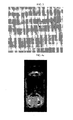
- FIG. 3 shows the shape of the cured composites of Comparative Example 1, and demonstrates that the composites lost their shape due to the formation of cracks during curing, unlike the composites prepared in Example 1.
- FIGs. 4a and 4b Optical microscopy images of the cured composites and monolith are shown in FIGs. 5 and 6 , respectively.
- FIGs. 4a and 4b demonstrate that shrinkage in the volume of the cured composites of Example 2 was much lower due to the presence of the long alkyl chains (as obtained from the bis(triethoxysilyl)octane used in the formation of the nanocrystal silica composite of Example 2)) than that of the cured monolith of Comparative Example 1.
- the images of FIGs. 5 and 6 show that no cracks were observed in the cured composites of Example 2 whereas cracks were observed in the cured monolith of Comparative Example 1.
Landscapes
- Chemical & Material Sciences (AREA)
- Engineering & Computer Science (AREA)
- Materials Engineering (AREA)
- Crystallography & Structural Chemistry (AREA)
- Organic Chemistry (AREA)
- Metallurgy (AREA)
- Inorganic Chemistry (AREA)
- Nanotechnology (AREA)
- General Physics & Mathematics (AREA)
- Physics & Mathematics (AREA)
- Condensed Matter Physics & Semiconductors (AREA)
- Dispersion Chemistry (AREA)
- General Chemical & Material Sciences (AREA)
- Manufacturing & Machinery (AREA)
- Chemical Kinetics & Catalysis (AREA)
- Composite Materials (AREA)
- Luminescent Compositions (AREA)
- Inorganic Compounds Of Heavy Metals (AREA)
Claims (14)
- Nanokristall-Metalloxid-Verbundwerkstoff, der einen Nanokristall und ein an den Nanokristall gebundenes Metalloxid umfasst, wobei das Metalloxid eine durch die Formel 1 dargestellte Verbindung ist:

R1 eine Alkylengruppe mit mindestens einem Kohlenstoffatom, eine Alkenylgruppe mit mindestens zwei Kohlenstoffatomen oder eine cyclische Gruppe mit mindestens drei Kohlenstoffatomen ist,
B eine oder mehrere sich wiederholende Einheit(en) ist, ausgewählt aus der Gruppe
bestehend aus

k eine ganze Zahl von1 bis 20 ist,
l, m und n jeweils unabhängig eine ganze Zahl einschließlich 0 ist und mindestens eines von l, m oder n größer als 0 ist und
x, y und z jeweils unabhängig eine ganze Zahl von 1 bis 3 ist. - Verbundwerkstoff nach Anspruch 1, wobei der Nanokristall ein Metall-Nanokristall oder ein Halbleiter-Nanokristall ist, ausgewählt aus der Gruppe bestehend aus Verbindungen der Gruppe 2-6, Verbindungen der Gruppe 3-5, Verbindungen der Gruppe 4-6, Verbindungen der Gruppe 4 und Gemischen derselben.
- Verbundwerkstoff nach Anspruch 2, wobei die Verbindungen der Gruppe 2-6 ausgewählt sind aus der Gruppe bestehend aus CdSe, CdTe, ZnS, ZnSe, ZnTe, ZnO, HgS,
HgSe, HgTe, CdSeS, CdSeTe, CdSTe, ZnSeS, ZnSeTe, ZnSTe, HgSeS, HgSeTe, HgSTe, CdZnS, CdZnSe, CdZnTe, CdHgS, CdHgSe, CdHgTe, HgZnS, HgZnSe, CdZnSeS, CdZnSeTe, CdZnSTe, CdHgSeS, CdHgSeTe, CdHgSTe, HgZnSeS, HgZnSeTe und HgZnSTe; die Verbindungen der Gruppe III-V ausgewählt sind aus der Gruppe bestehend aus GaN, GaP, GaAs, GaSb, AIN, AlP, AlAs, AlSb, InN, InP, InAs, InSb, GaNP, GaNAs, GaNSb, GaPAs, GaPSb, AINP, AINAs, AINSb, AIPAs, AIPSb, InNP, InNAs, InNSb, InPAs, InPSb, GaAlNP, GaAlNAs, GaAINSb, GaAlPAs, GaAIPSb, GalnNP, GalnNAs, GalnNSb, GalnPAs, GalnPSb, InAlNP, InAlNAs, InAlNSb, InAlPAs und InAlPSb; die Verbindungen der Gruppe IV-VI ausgewählt sind aus der Gruppe bestehend aus SnS, SnSe, SnTe, PbS, PbSe, PbTe, SnSeS, SnSeTe, SnSTe, PbSeS, PbSeTe, PbSTe, SnPbS, SnPbSe, SnPbTe, SnPbSSe, SnPbSeTe und SnPbSTe; und die Verbindungen der Gruppe IV ausgewählt sind aus der Gruppe bestehend aus Si, Ge, SiC und SiGe. - Leuchtdiodenvorrichtung, die Nanokristall-Metalloxid-Verbundwerkstoffe nach einem der Ansprüche 1 bis 3 umfasst.
- Verfahren zur Herstellung von Nanokristall-Metalloxid-Verbundwerkstoffen, wobei das Verfahren umfasst: Modifizieren der Oberfläche von Nanokristallen mit einem grenzflächenaktiven Stoff und Mischen des oberflächenmodifizierten Nanokristalls mit einem Metalloxidvorläufer mit organischen Gruppen, einem Lösungsmittel und Wasser zwecks Ausbildung eines Sol-Gels, wobei der grenzflächenaktive Stoff zur Reaktion mit dem Metalloxidvorläufer fähig ist und wobei das Metalloxid eine durch die Formel 1 dargestellte Verbindung ist:

R1 eine Alkylengruppe mit mindestens einem Kohlenstoffatom, eine Alkenylgruppe mit mindestens zwei Kohlenstoffatomen oder eine cyclische Gruppe mit mindestens drei Kohlenstoffatomen ist,
B eine oder mehrere sich wiederholende Einheit(en) ist, ausgewählt aus der Gruppe
bestehend aus

k eine ganze Zahl von1 bis 20 ist,
l, m und n jeweils unabhängig eine ganze Zahl einschließlich 0 ist und mindestens eines von l, m oder n größer als 0 ist und
x, y und z jeweils unabhängig eine ganze Zahl von 1 bis 3 ist. - Verfahren nach Anspruch 5, wobei die im ersten Schritt verwendeten Nanokristalle die von einem hydrophoben grenzflächenaktiven Stoff umgebenen sind.
- Verfahren nach Anspruch 5 oder 6, wobei während des Mischens ein zusätzlicher Metalloxidvorläufer zugegeben wird.
- Verfahren nach einem der Ansprüche 5-7, wobei das im zweiten Schritt verwendete Lösungsmittel ein polares Lösungsmittel ist, ausgewählt aus der Gruppe bestehend aus Alkanolen, Aceton, Ethylacetat, Dichlormethan, Chloroform, DMF, THF, DMSO, Pyridin und Alkylaminen.
- Verfahren nach einem der Ansprüche 5-8, wobei der Metalloxidvorläufer mit organischen Gruppen ausgewählt ist aus der Gruppe bestehend aus Organosiloxanverbindungen, Organosilanverbindungen, Silsesquioxanverbindungen, Titanoxiden, Aluminiumoxiden, Vanadiumoxiden, Zinkoxiden, Zinnoxiden, Tantaloxiden, Ceroxiden und Chromoxiden, mit organischen Gruppen.
- Verfahren nach Anspruch 9, wobei die Organosiloxanverbindungen ausgewählt sind aus der Gruppe bestehend aus Bis(triethoxysilyl)ethan, Bis(triethoxysilyl)butan, Bis(triethoxysilyl)octan, Bis(trimethoxysilyl)ethan, Bis(trimethoxysilyl)butan, Bis(trimethoxysilyl)octan, Bis-(triethoxysilyl)ethylen, Bis(trimethoxysilyl)ethylen, Bis(triethoxysilyl)acetylen, Bis(trimethoxysilyl)acetylen, 1,3,5-Tris(diethoxysila)cyclohexan und 1,3,5-Tris(triethoxysilyl)benzen.
- Verfahren nach Anspruch 9, wobei die Organosilanverbindungen ausgewählt sind aus der Gruppe bestehend aus Methyltrimethoxysilan, Dimethyldimethoxysilan, Propyltrimethoxysilan, Propyltriethoxysilan, Dipropyldimethoxysilan, Octyltrimethoxysilan, Octyltriethoxysilan, Dioctyldimethoxysilan und Hexadecyltriethoxysilan.
- Verfahren nach Anspruch 9, wobei die Silsesquioxanverbindung 2,4,6,8-Tetramethyl-2,4,6,8-tetra(trimethoxysilylethoxy)cyclotetrasiloxan ist.
- Verfahren nach einem der Ansprüche 5-12, wobei die Nanokristalle Metall-Nanokristalle oder Halbleiter-Nanokristalle sind, ausgewählt aus der Gruppe bestehend aus Verbindungen der Gruppe 2-6, Verbindungen der Gruppe 3-5, Verbindungen der Gruppe 4-6, Verbindungen der Gruppe 4 und Gemischen derselben.
- Verfahren zur Ausbildung eines Nanokristall-Metalloxid-Monolithen durch Verfestigen der durch das Verfahren nach einem der Ansprüche 5-13 hergestellten Verbundwerkstoffe in Sol-Gel-Form.
Applications Claiming Priority (3)
| Application Number | Priority Date | Filing Date | Title |
|---|---|---|---|
| KR20070089535 | 2007-09-04 | ||
| KR20070114329 | 2007-11-09 | ||
| KR1020080077613A KR101462654B1 (ko) | 2007-09-04 | 2008-08-07 | 나노결정-금속 산화물 복합체 및 그의 제조방법 |
Publications (3)
| Publication Number | Publication Date |
|---|---|
| EP2034002A2 EP2034002A2 (de) | 2009-03-11 |
| EP2034002A3 EP2034002A3 (de) | 2011-03-02 |
| EP2034002B1 true EP2034002B1 (de) | 2013-07-17 |
Family
ID=40042600
Family Applications (1)
| Application Number | Title | Priority Date | Filing Date |
|---|---|---|---|
| EP20080163169 Active EP2034002B1 (de) | 2007-09-04 | 2008-08-28 | Nanokristall-Metalloxid-Verbundstoffe und Herstellungsverfahren dafür |
Country Status (1)
| Country | Link |
|---|---|
| EP (1) | EP2034002B1 (de) |
Families Citing this family (9)
| Publication number | Priority date | Publication date | Assignee | Title |
|---|---|---|---|---|
| US7939363B1 (en) | 2010-10-27 | 2011-05-10 | General Electric Company | Systems and methods of intermixing cadmium sulfide layers and cadmium telluride layers for thin film photovoltaic devices |
| US7943415B1 (en) | 2010-10-27 | 2011-05-17 | Primestar Solar Inc. | Methods of sputtering cadmium sulfide layers for use in cadmium telluride based thin film photovoltaic devices |
| US8241930B2 (en) | 2011-05-31 | 2012-08-14 | Primestar Solar, Inc. | Methods of forming a window layer in a cadmium telluride based thin film photovoltaic device |
| US8247686B2 (en) | 2011-05-31 | 2012-08-21 | Primestar Solar, Inc. | Multi-layer N-type stack for cadmium telluride based thin film photovoltaic devices and methods of making |
| US8188562B2 (en) | 2011-05-31 | 2012-05-29 | Primestar Solar, Inc. | Multi-layer N-type stack for cadmium telluride based thin film photovoltaic devices and methods of making |
| US9054245B2 (en) | 2012-03-02 | 2015-06-09 | First Solar, Inc. | Doping an absorber layer of a photovoltaic device via diffusion from a window layer |
| DE102012102859A1 (de) | 2012-04-02 | 2013-11-14 | Osram Opto Semiconductors Gmbh | Optoelektronisches Bauelement umfassend eine Konverterträgerschicht, und Verfahren zur Herstellung eines optoelektronischen Bauelements umfassend eine Konverterträgerschicht |
| KR101463602B1 (ko) * | 2012-07-03 | 2014-11-20 | 주식회사 엘엠에스 | 캡슐화된 양자점 및 이를 이용한 장치 |
| CN110240126B (zh) * | 2019-06-14 | 2021-01-19 | 西安交通大学 | 一种纳米花结构的二硒化锡及其制备方法 |
Family Cites Families (5)
| Publication number | Priority date | Publication date | Assignee | Title |
|---|---|---|---|---|
| US5990479A (en) * | 1997-11-25 | 1999-11-23 | Regents Of The University Of California | Organo Luminescent semiconductor nanocrystal probes for biological applications and process for making and using such probes |
| US6207392B1 (en) * | 1997-11-25 | 2001-03-27 | The Regents Of The University Of California | Semiconductor nanocrystal probes for biological applications and process for making and using such probes |
| US7056471B1 (en) * | 2002-12-16 | 2006-06-06 | Agency For Science Technology & Research | Ternary and quarternary nanocrystals, processes for their production and uses thereof |
| EP1733077B1 (de) * | 2004-01-15 | 2018-04-18 | Samsung Electronics Co., Ltd. | Nanokristalldotierte matrizes |
| US20100119697A1 (en) * | 2006-05-10 | 2010-05-13 | 3M Innovative Properties Company | Compositions and coatings containing fluorescent, inorganic nanoparticles |
-
2008
- 2008-08-28 EP EP20080163169 patent/EP2034002B1/de active Active
Also Published As
| Publication number | Publication date |
|---|---|
| EP2034002A2 (de) | 2009-03-11 |
| EP2034002A3 (de) | 2011-03-02 |
Similar Documents
| Publication | Publication Date | Title |
|---|---|---|
| EP2034002B1 (de) | Nanokristall-Metalloxid-Verbundstoffe und Herstellungsverfahren dafür | |
| KR101874413B1 (ko) | 무기 리간드를 갖는 양자점 및 그의 제조방법 | |
| KR101462655B1 (ko) | 나노결정-금속 산화물 복합체의 제조방법 및 그에 의해 제조된 나노결정-금속 산화물 복합체 | |
| US8237154B2 (en) | Composite light-emitting material and light-emitting device comprising the same | |
| US9082982B2 (en) | Semiconductor nanocrystal-polymer composite, method of preparing the same, and composite film and optoelectronic device including the same | |
| CN108219769B (zh) | 发射性纳米晶体颗粒、其制备方法和包括发射性纳米晶体颗粒的器件 | |
| US7927515B2 (en) | Nanocrystal-metal oxide-polymer composites and preparation method thereof | |
| EP2028248A1 (de) | Nanokristallmischung und Leuchtdiode damit | |
| US9193900B2 (en) | Optoelectronic device and stacking structure | |
| KR101695005B1 (ko) | 나노결정/수지 조성물, 나노결정-수지 복합체 및 나노결정-수지 복합체의 제조방법 | |
| US8362504B2 (en) | Light emitting diode device using nanocrystal-metal oxide composite and method for fabricating the same | |
| US20070110816A1 (en) | Method of coating nanoparticles | |
| KR20150107469A (ko) | 나노입자 중합체 | |
| TW201807159A (zh) | 包括半導體奈米結晶之複合物及其製備方法 | |
| KR20150016436A (ko) | 마그네슘-셀레나이드 나노 결정 합성 방법 | |
| US8092719B2 (en) | Nanocrystal-metal oxide composites and preparation method thereof | |
| KR101841616B1 (ko) | 반도체 나노결정 실록산 복합체 수지 조성물 및 그 제조방법 | |
| KR102488237B1 (ko) | 양자점, 이를 포함하는 양자점 발광다이오드, 양자점 필름, 광 변환 수지 조성물, 상기 광 변환 수지 조성물을 이용하여 형성되는 컬러필터, 광 변환 적층기재 및 상기 컬러필터 또는 상기 광 변환 적층기재를 포함하는 화상표시장치 | |
| KR20210033160A (ko) | 양자점-고분자 복합체 입자 및 이의 제조방법 | |
| KR101823546B1 (ko) | 반도체 나노결정-고분자 조성물, 반도체 나노결정-고분자 복합체, 이의 제조방법 및 이를 포함하는 필름과 광전자 소자 | |
| KR102488238B1 (ko) | 양자점, 이를 포함하는 양자점 발광다이오드, 양자점 필름, 광 변환 수지 조성물, 상기 광 변환 수지 조성물을 이용하여 형성되는 컬러필터, 광 변환 적층기재 및 상기 컬러필터 또는 상기 광 변환 적층기재를 포함하는 화상표시장치 | |
| KR101755656B1 (ko) | 나노결정/수지 조성물 또는 나노결정-수지 복합체를 포함하는 소자 | |
| KR102193724B1 (ko) | 표면 개질된 무기나노발광체 및 이의 제조방법 | |
| KR102488304B1 (ko) | 양자점, 이를 포함하는 양자점 발광다이오드, 양자점 필름, 광 변환 수지 조성물, 상기 광 변환 수지 조성물을 이용하여 형성되는 컬러필터, 광 변환 적층기재 및 상기 컬러필터 또는 상기 광 변환 적층기재를 포함하는 화상표시장치 |
Legal Events
| Date | Code | Title | Description |
|---|---|---|---|
| PUAI | Public reference made under article 153(3) epc to a published international application that has entered the european phase |
Free format text: ORIGINAL CODE: 0009012 |
|
| AK | Designated contracting states |
Kind code of ref document: A2 Designated state(s): AT BE BG CH CY CZ DE DK EE ES FI FR GB GR HR HU IE IS IT LI LT LU LV MC MT NL NO PL PT RO SE SI SK TR |
|
| AX | Request for extension of the european patent |
Extension state: AL BA MK RS |
|
| PUAL | Search report despatched |
Free format text: ORIGINAL CODE: 0009013 |
|
| AK | Designated contracting states |
Kind code of ref document: A3 Designated state(s): AT BE BG CH CY CZ DE DK EE ES FI FR GB GR HR HU IE IS IT LI LT LU LV MC MT NL NO PL PT RO SE SI SK TR |
|
| AX | Request for extension of the european patent |
Extension state: AL BA MK RS |
|
| RIC1 | Information provided on ipc code assigned before grant |
Ipc: C09K 11/88 20060101AFI20081203BHEP Ipc: C30B 5/00 20060101ALI20110126BHEP Ipc: C30B 29/54 20060101ALI20110126BHEP Ipc: C09K 11/56 20060101ALI20110126BHEP Ipc: C30B 7/00 20060101ALI20110126BHEP Ipc: C30B 29/46 20060101ALI20110126BHEP Ipc: C30B 29/48 20060101ALI20110126BHEP Ipc: C30B 29/50 20060101ALI20110126BHEP |
|
| 17P | Request for examination filed |
Effective date: 20110902 |
|
| AKX | Designation fees paid |
Designated state(s): DE FR GB |
|
| GRAC | Information related to communication of intention to grant a patent modified |
Free format text: ORIGINAL CODE: EPIDOSCIGR1 |
|
| GRAP | Despatch of communication of intention to grant a patent |
Free format text: ORIGINAL CODE: EPIDOSNIGR1 |
|
| RIC1 | Information provided on ipc code assigned before grant |
Ipc: C09K 11/88 20060101AFI20120530BHEP Ipc: C09K 11/59 20060101ALI20120530BHEP Ipc: C30B 7/00 20060101ALI20120530BHEP Ipc: B82Y 30/00 20110101ALI20120530BHEP Ipc: B82Y 40/00 20110101ALI20120530BHEP Ipc: C30B 29/54 20060101ALI20120530BHEP Ipc: C09K 11/56 20060101ALI20120530BHEP Ipc: C30B 29/46 20060101ALI20120530BHEP Ipc: C30B 29/60 20060101ALI20120530BHEP Ipc: C30B 5/00 20060101ALI20120530BHEP Ipc: C30B 29/50 20060101ALI20120530BHEP Ipc: C30B 7/14 20060101ALI20120530BHEP Ipc: C30B 29/48 20060101ALI20120530BHEP |
|
| RAP1 | Party data changed (applicant data changed or rights of an application transferred) |
Owner name: SAMSUNG ELECTRONICS CO., LTD. |
|
| GRAP | Despatch of communication of intention to grant a patent |
Free format text: ORIGINAL CODE: EPIDOSNIGR1 |
|
| GRAS | Grant fee paid |
Free format text: ORIGINAL CODE: EPIDOSNIGR3 |
|
| GRAA | (expected) grant |
Free format text: ORIGINAL CODE: 0009210 |
|
| AK | Designated contracting states |
Kind code of ref document: B1 Designated state(s): DE FR GB |
|
| REG | Reference to a national code |
Ref country code: GB Ref legal event code: FG4D |
|
| REG | Reference to a national code |
Ref country code: DE Ref legal event code: R096 Ref document number: 602008026019 Country of ref document: DE Effective date: 20130912 |
|
| PLBE | No opposition filed within time limit |
Free format text: ORIGINAL CODE: 0009261 |
|
| STAA | Information on the status of an ep patent application or granted ep patent |
Free format text: STATUS: NO OPPOSITION FILED WITHIN TIME LIMIT |
|
| 26N | No opposition filed |
Effective date: 20140422 |
|
| REG | Reference to a national code |
Ref country code: DE Ref legal event code: R097 Ref document number: 602008026019 Country of ref document: DE Effective date: 20140422 |
|
| REG | Reference to a national code |
Ref country code: FR Ref legal event code: PLFP Year of fee payment: 9 |
|
| REG | Reference to a national code |
Ref country code: FR Ref legal event code: PLFP Year of fee payment: 10 |
|
| REG | Reference to a national code |
Ref country code: FR Ref legal event code: PLFP Year of fee payment: 11 |
|
| P01 | Opt-out of the competence of the unified patent court (upc) registered |
Effective date: 20230530 |
|
| PGFP | Annual fee paid to national office [announced via postgrant information from national office to epo] |
Ref country code: DE Payment date: 20250708 Year of fee payment: 18 |
|
| PGFP | Annual fee paid to national office [announced via postgrant information from national office to epo] |
Ref country code: GB Payment date: 20250710 Year of fee payment: 18 |
|
| PGFP | Annual fee paid to national office [announced via postgrant information from national office to epo] |
Ref country code: FR Payment date: 20250708 Year of fee payment: 18 |