EP2034505A2 - Écran d'affichage à plasma et procédé de formation de ces électrodes - Google Patents
Écran d'affichage à plasma et procédé de formation de ces électrodes Download PDFInfo
- Publication number
- EP2034505A2 EP2034505A2 EP08252941A EP08252941A EP2034505A2 EP 2034505 A2 EP2034505 A2 EP 2034505A2 EP 08252941 A EP08252941 A EP 08252941A EP 08252941 A EP08252941 A EP 08252941A EP 2034505 A2 EP2034505 A2 EP 2034505A2
- Authority
- EP
- European Patent Office
- Prior art keywords
- electrodes
- substrate
- plasma display
- display panel
- address
- Prior art date
- Legal status (The legal status is an assumption and is not a legal conclusion. Google has not performed a legal analysis and makes no representation as to the accuracy of the status listed.)
- Withdrawn
Links
Images


Classifications
-
- H—ELECTRICITY
- H01—ELECTRIC ELEMENTS
- H01J—ELECTRIC DISCHARGE TUBES OR DISCHARGE LAMPS
- H01J11/00—Gas-filled discharge tubes with alternating current induction of the discharge, e.g. alternating current plasma display panels [AC-PDP]; Gas-filled discharge tubes without any main electrode inside the vessel; Gas-filled discharge tubes with at least one main electrode outside the vessel
- H01J11/20—Constructional details
- H01J11/34—Vessels, containers or parts thereof, e.g. substrates
-
- H—ELECTRICITY
- H01—ELECTRIC ELEMENTS
- H01J—ELECTRIC DISCHARGE TUBES OR DISCHARGE LAMPS
- H01J9/00—Apparatus or processes specially adapted for the manufacture, installation, removal, maintenance of electric discharge tubes, discharge lamps, or parts thereof; Recovery of material from discharge tubes or lamps
- H01J9/02—Manufacture of electrodes or electrode systems
-
- H—ELECTRICITY
- H01—ELECTRIC ELEMENTS
- H01J—ELECTRIC DISCHARGE TUBES OR DISCHARGE LAMPS
- H01J11/00—Gas-filled discharge tubes with alternating current induction of the discharge, e.g. alternating current plasma display panels [AC-PDP]; Gas-filled discharge tubes without any main electrode inside the vessel; Gas-filled discharge tubes with at least one main electrode outside the vessel
- H01J11/10—AC-PDPs with at least one main electrode being out of contact with the plasma
- H01J11/12—AC-PDPs with at least one main electrode being out of contact with the plasma with main electrodes provided on both sides of the discharge space
-
- H—ELECTRICITY
- H01—ELECTRIC ELEMENTS
- H01J—ELECTRIC DISCHARGE TUBES OR DISCHARGE LAMPS
- H01J11/00—Gas-filled discharge tubes with alternating current induction of the discharge, e.g. alternating current plasma display panels [AC-PDP]; Gas-filled discharge tubes without any main electrode inside the vessel; Gas-filled discharge tubes with at least one main electrode outside the vessel
- H01J11/20—Constructional details
- H01J11/22—Electrodes, e.g. special shape, material or configuration
- H01J11/24—Sustain electrodes or scan electrodes
-
- H—ELECTRICITY
- H01—ELECTRIC ELEMENTS
- H01J—ELECTRIC DISCHARGE TUBES OR DISCHARGE LAMPS
- H01J11/00—Gas-filled discharge tubes with alternating current induction of the discharge, e.g. alternating current plasma display panels [AC-PDP]; Gas-filled discharge tubes without any main electrode inside the vessel; Gas-filled discharge tubes with at least one main electrode outside the vessel
- H01J11/20—Constructional details
- H01J11/22—Electrodes, e.g. special shape, material or configuration
- H01J11/26—Address electrodes
-
- H—ELECTRICITY
- H01—ELECTRIC ELEMENTS
- H01J—ELECTRIC DISCHARGE TUBES OR DISCHARGE LAMPS
- H01J2211/00—Plasma display panels with alternate current induction of the discharge, e.g. AC-PDPs
- H01J2211/20—Constructional details
- H01J2211/22—Electrodes
- H01J2211/24—Sustain electrodes or scan electrodes
- H01J2211/245—Shape, e.g. cross section or pattern
-
- H—ELECTRICITY
- H01—ELECTRIC ELEMENTS
- H01J—ELECTRIC DISCHARGE TUBES OR DISCHARGE LAMPS
- H01J2211/00—Plasma display panels with alternate current induction of the discharge, e.g. AC-PDPs
- H01J2211/20—Constructional details
- H01J2211/22—Electrodes
- H01J2211/26—Address electrodes
- H01J2211/265—Shape, e.g. cross section or pattern
-
- H—ELECTRICITY
- H01—ELECTRIC ELEMENTS
- H01J—ELECTRIC DISCHARGE TUBES OR DISCHARGE LAMPS
- H01J2211/00—Plasma display panels with alternate current induction of the discharge, e.g. AC-PDPs
- H01J2211/20—Constructional details
- H01J2211/22—Electrodes
- H01J2211/32—Disposition of the electrodes
- H01J2211/323—Mutual disposition of electrodes
Definitions
- the present invention relates to a plasma display panel, and more particularly, to a method of forming an electrode of a plasma display panel capable of preventing short circuit between electrodes, and a plasma display panel manufactured according to this method.
- Plasma display panel is an electron apparatus that displays an image using plasma discharge.
- the plasma display panel displays an image by applying a predetermined voltage to electrodes disposed in a discharge space of the plasma display panel to cause a plasma discharge between the electrodes and exciting a phosphor layer formed with a predetermined pattern by the ultraviolet rays generated during the plasma discharge.
- a plurality of row electrodes and a plurality of column electrodes are formed in the plasma display panel of the plasma display apparatus, and discharge cells are formed in positions where row electrodes and column electrodes are crossed with each other.
- Plasma display panels represent grey levels of the image by controlling a discharging state of the discharge cells.
- the offset printing process has a very high possibility that short circuit occurs between neighboring electrodes due to an expansion in volume of material forming electrodes at the end points of the electrodes during a transfer process.
- a plasma display panel as claimed in Claim 15.
- a preferred feature of this plasma display panel is set out in Claim 16.
- a plasma display panel including a first substrate and a second substrate disposed to face each other; address electrodes formed on the second substrate; a barrier rib for compartmentalizing a plurality of discharge cells disposed in a space between the first substrate and the second substrate to form a display region; a phosphor layer formed inside each of the discharge cells; and sustain electrodes and scan electrodes formed on the first substrate to extend in a direction that crosses a direction in which the address electrodes extend, wherein end points of the neighboring address electrodes extend to different longitudinal positions so as to be longitudinally offset relative to each other to have a longitudinal positional difference.
- the plasma display panel may further include address drivers coupled to the other ends of the address electrodes.
- the address electrodes may include even-numbered address electrodes and odd-numbered address electrodes where ends of the odd-numbered address electrodes have the longitudinal positional difference compared to the ends of the even-numbered address electrodes.
- the odd numbered address electrodes extend to a first longitudinal position and the even numbered address electrodes extend to a second longitudinal position different from the first longitudinal position, so that ends of the odd numbered address electrodes are longitudinally offset from ends of even numbered address electrodes by the longitudinal positional difference.
- the address electrodes may be formed using an offset printing process.
- a plasma display panel including a first substrate and a second substrate disposed to face each other; address electrodes formed on the second substrate; a barrier rib for compartmentalizing a plurality of discharge cells disposed in a space between the first substrate and the second substrate to form a display region; a phosphor layer formed inside each of the discharge cells; and sustain electrodes and scan electrodes formed on the first substrate to extend in a direction that crosses a direction in which the address electrodes extend and disposed to alternate a pair of scan electrodes and a pair of sustain electrodes, wherein ends of either the pair of the scan electrodes or the pair of the sustain electrodes or both extend to a different longitudinal position to be longitudinally offset relative to each other to have a longitudinal positional difference.
- the sustain electrodes and/or scan electrodes having said longitudinal positional difference are metallic bus electrodes, said scan and/or sustain electrodes each further comprising a transparent electrode electrically connected to the sustain and/or scan electrode respectively.
- the longitudinal positional difference may not be applied to these transparent electrodes.
- the plasma display panel may further include scan drivers coupled to the other ends of the scan electrodes; and sustain drivers coupled to the other ends of the sustain electrodes.
- the scan electrodes and the sustain electrodes may be formed using an offset printing process.
- a method of forming an electrode of a plasma display panel including steps of forming concave grooves, which are flat in one direction, that is they extend linearly in the one direction, in a gravure; filling the concave grooves with an electrode-forming paste; transiting the paste from the concave grooves to a print blanket; and transferring the paste from the print blanket onto a substrate of the plasma display panel, wherein ends of the neighboring concave grooves on the gravure have a longitudinal positional difference.
- the gravure may be a plate gravure or, a roller-type gravure.
- the electrodes may be address electrodes of the plasma display panel.
- the substrate becomes a lower substrate of the plasma display panel.
- the address electrodes are preferably made of metallic materials.
- the electrodes may be scan electrodes and sustain electrodes of the plasma display panel, or metallic bus electrodes included in the scan electrodes and sustain electrodes of the plasma display panel.
- the substrate becomes an upper substrate of the plasma display panel, and the plasma display panel may preferably have an electrode array disposed to alternate a pair of scan electrodes and a pair of sustain electrodes.
- FIG. 1 is a perspective view showing one exemplary embodiment of a plasma display panel
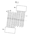
- FIG. 2 is a partial top view showing a configuration of an address electrode of a plasma display panel constructed according to one exemplary embodiment of the present invention
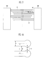
- FIG. 3 is a partial top view showing a configuration of scan and sustain electrodes of a plasma display panel constructed according to another exemplary embodiment of the present invention
- FIGS. 4A to 4C are conceptual diagrams comparing a positional difference between end points of electrodes in a longitudinal direction according to preferred embodiments of the present invention with that of the contemporary electrodes, and illustrating the preferable positional difference range;
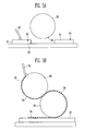
- FIG. 5A is a cross-sectional view showing one exemplary embodiment of an apparatus of forming an electrode of a plasma display panel that is applicable to still another embodiment of the present invention.
- FIG. 5B is a cross-sectional view showing another exemplary embodiment of an apparatus for forming an electrode of a plasma display panel.
- a plurality of discharge cells arranged in a matrix type are interposed between upper and lower substrates having scan electrodes and sustain electrodes causing mutual discharge and a plurality of address electrodes, all of which are disposed in the upper and lower substrates, and the facing upper and lower substrates are then attached to each other.
- a predetermined amount of discharge gas is injected between both substrates, and a predetermined discharge pulse is then applied between discharge electrodes to excite a phosphor applied inside the discharge cells. Then the excited phosphor is allowed to emit the visible light, and the plasma display panel uses the generated visible light to display a predetermined image.
- the electrodes of a plasma display panel may be easily formed at a low manufacturing cost by transferring an electrode-forming material to a substrate using an offset printing process. At this time, an expansion in volume of material forming electrode can occur in one end of the heated electrode-forming material. This end of the heated electrode-forming material accordingly has a greater width than other regions of the electrodes. If the expansion phenomenon occurs in two adjacent positions of two adjacent electrodes, there is an increasing risk of the short between the corresponding electrodes.
- ends of electrodes in the same group that are present in the same position in the art have a positional difference in length compared to ends of neighboring electrodes.
- adjacent electrodes from different groups extend to different longitudinal positions so as to be longitudinally offset relative to each other.
- the ends of the electrodes may be arranged in a variety of configurations.
- a configuration where ends of the electrodes having the positional difference in length are disposed in a zig-zag manner, is, however, preferred to reduce a wasted area of the substrate.
- Plasma display panels may be of AC type, DC type and a hybrid type, depending on their configuration.
- FIG. 1 shows an AC type plasma display panel.
- the plasma display panel includes a lower substrate 4; address electrodes 2 formed on lower substrate 4; a dielectric layer 6 formed on lower substrate 4 having address electrode 2 formed therein; a barrier rib 5 is formed on dielectric layer 6 to maintain a discharge distance and prevent cross talks between cells; and a phosphor layer 1 is formed on a surface of barrier rib 5.
- the plasma display panel includes scan electrodes 11 and sustain electrodes 12 formed in upper substrate 10. Scan electrodes 11 and sustain electrodes 12 are disposed perpendicular to address electrodes 2, and one discharge cell therefore corresponds to a pair of the crossed electrodes. A dielectric layer 9 and a passivation layer 3 are formed in order to cover scan electrodes 11 and sustain electrodes 12.
- Scan electrode 11 and sustain electrode 12 are disposed spaced apart at a predetermined distance along one direction of upper substrate 10.
- each of scan electrodes 11 and/or sustain electrodes 12 may be formed with combinations of transparent electrodes 11-2, 12-2 and metallic bus electrodes 11-1, 12-1 as shown in FIG. 1 , transparent electrodes 11-2, 12-2 being formed of transparent materials such ITO, and metallic bus electrodes 11-1, 12-1 being respectively electrically coupled to transparent electrodes 11-2, 12-2.
- This dual electrode structure has the advantage that the entire electrode resistance may be lowered by forming bus electrodes 11-1, 12-1 using highly conductive materials, such as Ag, as a raw material since it is difficult for transparent electrodes 11-2, 12-2 to transmit an electric current because transparent electrodes 11-2, 12-2 for transmitting discharge light in the discharge cells is thin and has a high resistance.
- a dielectric layer 9 and an MgO passivation layer 3 are laminated on upper substrate 10 while covering scan electrodes 11 and sustain electrodes 12.
- address electrodes 2 are formed on lower substrate 4 coupled to upper substrate 10, address electrodes 2 being crossed at a right angle with scan electrodes 11 and sustain electrodes 12, and a dielectric layer 6 is formed on lower substrate 4 while covering address electrodes 2.
- a barrier rib 5 that compartmentalize a plurality of discharge spaces is formed between upper substrate 10 and lower substrate 4, and phosphor layers 1 is formed on side walls of barrier rib 5 disposed inside the discharge space, and also formed on dielectric layer 6, with the phosphor layers being composed of R, G and B phosphors.
- the plasma display panel may be manufactured as one display device by applying frit as an adhesive means around upper substrate 10 and lower substrate 4 while each of the above-mentioned components is formed on either upper substrate 10 or lower substrate 4, followed by undergoing sealing and exhaust processes, etc.
- FIG. 2 shows a configuration of an address electrode of the plasma display panel constructed as one exemplary embodiment of the present invention.
- address electrodes 2 are grouped into a predetermined number of address electrodes and the ends of each group of address electrodes are coupled to one address driver 200.
- address drivers 200 may be alternately disposed in two opposite portions of a plasma display panel, i.e., an upper portion and a lower portion of a chassis base on which a plasma display panel is attached.
- This arrangement of the address drivers 200 serves merely to enhance drive uniformity of the address drivers 200 and facilitate the disposition of the address drivers 200 if it has a high resolution.It is, however, understood that the present invention is not limited to this arrangement and extends also to arrangements where address drivers are disposed only in either an upper portion or a lower portion of the panel.
- Each address electrode comes to an end on the substrate in an end point.
- the other end of each of the address electrodes is coupled to address driver 200.
- the ends of even-numbered electrodes and ends of odd-numbered electrodes extend to different longitudinal positions, so that even and odd numbered electrodes have a longitudinal positional difference.
- the longitudinal positional difference is maintained between the even and odd numbered electrodes in a longitudinal direction of the electrodes at a predetermined distance.
- the longitudinal positional difference of two neighboring electrodes in the end point of each of the address electrode pairs is preferably similar to the distance between two neighboring address electrodes.
- distance A1 may be similar to distance B1 as shown in FIG. 2 .
- a preferable value of the longitudinal positional difference will be calculated, as follows.
- FIG. 3 shows a configuration of scan/sustain electrodes of a 3-electrode surface discharge plasma display panel according to one exemplary embodiment of the present invention.
- a scan electrode pair and a sustain electrode pair have an alternating XXYY-type electrode array, a scan driver 300 electrically coupled to the scan electrodes to drive scan electrodes 11 is disposed in one side of the panel, and a sustain driver 400 coupled to sustain electrodes 12 to drive the sustain electrodes is disposed in an opposite side of the panel. That is to say, an end point where an electrode comes to an end on the substrate is formed in one end of each of the scan electrodes and the sustain electrodes, and the other ends of each of scan electrodes 11 and sustain electrodes 12 is respectively electrically coupled to scan drivers 300 and sustain driver 400.
- Each of the scan electrodes and sustain electrodes as shown in FIG. 3 may comprise a transparent electrode and a bus electrode, as shown in FIG. 1 .
- a transparent electrode and a bus electrode as shown in FIG. 1 .
- this expansion phenomenon causes a short circuit between the bus electrodes. Since materials of the bus electrode are opaque each of the bus electrode pairs is disposed toward the barrier rib as close as possible. This leads to a further increased risk of short circuiting in the case of the high-definition panel.
- end points of the bus electrodes are formed at different positions in a longitudinal direction of the electrodes. Therefore, although the bus electrodes are formed using an offset printing process, the short circuit induced by the solution lumping in the end points may be effectively prevented during the manufacturing process.
- the positional difference in a longitudinal direction of the electrodes in the end points of each of the bus electrode pairs is preferably similar to the distance between electrodes forming pairs. In other words, distance A2 may be similar to distance B2 as shown in FIG. 3 .
- the risk of a short circuit being created by solution lumping may be increased when the longitudinal positional difference in each of the bus electrodes of the HD plasma display panel is less than 20 ⁇ m, while an effect of preventing short circuits created through solution lumping may not be further improved when the longitudinal positional difference exceeds 100 ⁇ m.
- the expansion phenomenon occurs in the end point of the electrode, and therefore the end point of the electrode is created with a round shape that is wider than the (initial) width (d) of the electrode.
- an end point diffusion width (c) created by the expansion phenomenon is equal to or greater than half of the spacing distance (a0) between the electrodes a short circuit between the electrodes may be generated.
- the short circuit between the electrodes may be prevented until the end point diffusion width (c) created by the expansion phenomenon becomes equal to the spacing distance (a0) between the electrodes.
- Distance (a) refers to a distance between central longitudinal axes of two neighboring electrodes.
- the longitudinal positional difference (w) between end points of two electrodes is sufficient if the longitudinal positional difference (w) satisfies the following Equation (1):
- w longitudinal positional difference
- a is a distance between central axes of two neighboring electrodes
- c is a diffusion width created by solution lumping process
- d is an (initial) width of electrode.
- c can also be expressed as half the difference between d and the width of the enlarged end of the electrode.
- FIG. 5A is a cross-sectional view showing one exemplary embodiment of an apparatus of forming an electrode of a plasma display panel constructed to one embodiment of the present invention
- FIG. 5B is a cross-sectional view showing another exemplary embodiment of an apparatus of forming an electrode of a plasma display panel according to one embodiment of the present invention.
- scan/sustain electrodes and address electrodes are formed on upper or lower substrates by employing the following offset printing process.
- the scan/sustain electrodes have a dual electrode structure of transparent electrodes and bus electrodes, the offset printing process is applicable to the bus electrodes.
- the method of forming electrodes is carried out, including steps of forming concave grooves, which extend linearly in one direction, in a gravure; filling the concave grooves with an electrode-forming paste; transiting the paste from the concave grooves to a print blanket; and transferring the paste from the print blanket onto a substrate of the plasma display panel.
- a gravure having concave grooves for forming an electrode should be prepared in a gravure plate 31.
- One end, in which end points is formed, of each of the concave grooves formed on the gravure may be realized to have a predetermined longitudinal positional difference from ends of neighboring concave grooves.
- the concave grooves on gravure plate 31 are filled with an electrode-forming paste 34, and overflown paste 34 is removed using a blade 32.
- paste 34 filled in the concave groove 33 of gravure plate 31 is transited to a print blanket 35.
- Transited paste 34 is transferred to a glass substrate 37 constituting a panel.
- glass substrate 37 is dried and sintered to complete the electrode-forming process.
- FIG. 5A is a conceptual diagram schematically showing steps of forming a concave groove 33 in a gravure plate 31, filling concave groove 33 with paste and transferring the pasted into a glass substrate.
- FIG. 5B is a conceptual diagram schematically showing steps of forming a concave groove in a gravure roller 39, filling concave groove 33 with paste, transferring the paste onto printed blanket 35 and further onto glass substrate 37.
- the concave groove according to this exemplary embodiment is formed in a gravure plate 31 or a gravure roll 35, and then filled with paste, and the paste is transited to blanket 35, and then transferred to glass substrate 37.
- the glass substrate 37 constitutes an upper substrate or a lower substrate.
- the method of forming an electrode of a plasma display panel according to preferred embodiments of the present invention, as described above, may be useful to prevent the short of the electrode during the process.
- the method may be useful to prevent the short of the electrode in the process that is widely used for forming an electrode of the plasma display panel.
Landscapes
- Engineering & Computer Science (AREA)
- Physics & Mathematics (AREA)
- Plasma & Fusion (AREA)
- Chemical & Material Sciences (AREA)
- Materials Engineering (AREA)
- Manufacturing & Machinery (AREA)
- Gas-Filled Discharge Tubes (AREA)
Applications Claiming Priority (1)
| Application Number | Priority Date | Filing Date | Title |
|---|---|---|---|
| KR1020070090458A KR100893471B1 (ko) | 2007-09-06 | 2007-09-06 | 플라즈마 디스플레이 패널 및 그 전극 형성 방법 |
Publications (2)
| Publication Number | Publication Date |
|---|---|
| EP2034505A2 true EP2034505A2 (fr) | 2009-03-11 |
| EP2034505A3 EP2034505A3 (fr) | 2010-05-19 |
Family
ID=40085402
Family Applications (1)
| Application Number | Title | Priority Date | Filing Date |
|---|---|---|---|
| EP08252941A Withdrawn EP2034505A3 (fr) | 2007-09-06 | 2008-09-04 | Écran d'affichage à plasma et procédé de formation de ces électrodes |
Country Status (5)
| Country | Link |
|---|---|
| US (1) | US20090072739A1 (fr) |
| EP (1) | EP2034505A3 (fr) |
| JP (1) | JP2009064765A (fr) |
| KR (1) | KR100893471B1 (fr) |
| CN (1) | CN101383257B (fr) |
Family Cites Families (5)
| Publication number | Priority date | Publication date | Assignee | Title |
|---|---|---|---|---|
| FR2761510B1 (fr) * | 1997-03-27 | 1999-04-30 | Bull Sa | Ecran et montage des circuits de commande des pixels de l'ecran |
| KR100404200B1 (ko) * | 2001-07-12 | 2003-11-03 | 엘지전자 주식회사 | 유기 el 디스플레이 패널 |
| KR100573140B1 (ko) * | 2004-04-16 | 2006-04-24 | 삼성에스디아이 주식회사 | 플라즈마 디스플레이 패널 |
| KR100560485B1 (ko) * | 2004-06-30 | 2006-03-13 | 삼성에스디아이 주식회사 | 플라즈마 디스플레이 패널의 전극 인쇄장치 및 이를이용한 플라즈마 디스플레이 패널의 제조방법 |
| KR101057121B1 (ko) * | 2004-09-03 | 2011-08-16 | 엘지전자 주식회사 | 플라즈마 디스플레이 패널의 전극 패드 구조 |
-
2007
- 2007-09-06 KR KR1020070090458A patent/KR100893471B1/ko not_active Ceased
- 2007-11-09 JP JP2007292274A patent/JP2009064765A/ja not_active Withdrawn
-
2008
- 2008-09-04 US US12/230,804 patent/US20090072739A1/en not_active Abandoned
- 2008-09-04 EP EP08252941A patent/EP2034505A3/fr not_active Withdrawn
- 2008-09-08 CN CN2008102157628A patent/CN101383257B/zh not_active Withdrawn - After Issue
Also Published As
| Publication number | Publication date |
|---|---|
| CN101383257A (zh) | 2009-03-11 |
| CN101383257B (zh) | 2010-06-23 |
| KR100893471B1 (ko) | 2009-04-17 |
| EP2034505A3 (fr) | 2010-05-19 |
| KR20090025533A (ko) | 2009-03-11 |
| JP2009064765A (ja) | 2009-03-26 |
| US20090072739A1 (en) | 2009-03-19 |
Similar Documents
| Publication | Publication Date | Title |
|---|---|---|
| US5754003A (en) | Discharger display device having means for air-tight separation of discharge chambers by partition walls, and process of producing the same | |
| KR100794076B1 (ko) | 가스방전 표시장치와 그 제조방법 | |
| KR100326110B1 (ko) | 표시 패널 및 그 구동 방법 | |
| JP2003045337A (ja) | 表示管および表示装置 | |
| JPH052993A (ja) | 面放電型プラズマデイスプレイパネル及びその駆動方法 | |
| JP2001052623A (ja) | ガス放電表示装置とその製造方法 | |
| JPH07262930A (ja) | 面放電型ガス放電パネル | |
| US20070188413A1 (en) | Plasma display device | |
| JP2001243883A (ja) | ガス放電パネルおよびガス放電デバイスとその製造方法 | |
| EP2034505A2 (fr) | Écran d'affichage à plasma et procédé de formation de ces électrodes | |
| JP4664542B2 (ja) | ガス放電表示装置 | |
| KR100453163B1 (ko) | 플라즈마 디스플레이 패널 | |
| US7701414B2 (en) | Plasma display panel and method of driving the same | |
| EP1748461A1 (fr) | Panneau d'affichage plasma et son procede d'entrainement | |
| JP4465339B2 (ja) | 単色表示に適したプラズマディスプレイ装置 | |
| KR100719593B1 (ko) | 플라즈마 디스플레이 패널 | |
| KR100466278B1 (ko) | 플라즈마 디스플레이 패널 | |
| EP1734496A1 (fr) | Écran de type faisceau de tube à arc et sa méthode de direction | |
| JP4003873B2 (ja) | プラズマディスプレイパネル | |
| JP3937563B2 (ja) | Ac型プラズマディスプレイパネル | |
| KR100563054B1 (ko) | 플라즈마 디스플레이 패널 | |
| US20090026954A1 (en) | Plasma display panel | |
| KR100869412B1 (ko) | 플라즈마 디스플레이 패널 | |
| KR100426578B1 (ko) | 플라즈마 표시 패널 | |
| JP2008300297A (ja) | ディスプレイパネル |
Legal Events
| Date | Code | Title | Description |
|---|---|---|---|
| PUAI | Public reference made under article 153(3) epc to a published international application that has entered the european phase |
Free format text: ORIGINAL CODE: 0009012 |
|
| 17P | Request for examination filed |
Effective date: 20080910 |
|
| AK | Designated contracting states |
Kind code of ref document: A2 Designated state(s): AT BE BG CH CY CZ DE DK EE ES FI FR GB GR HR HU IE IS IT LI LT LU LV MC MT NL NO PL PT RO SE SI SK TR |
|
| AX | Request for extension of the european patent |
Extension state: AL BA MK RS |
|
| PUAL | Search report despatched |
Free format text: ORIGINAL CODE: 0009013 |
|
| AK | Designated contracting states |
Kind code of ref document: A3 Designated state(s): AT BE BG CH CY CZ DE DK EE ES FI FR GB GR HR HU IE IS IT LI LT LU LV MC MT NL NO PL PT RO SE SI SK TR |
|
| AX | Request for extension of the european patent |
Extension state: AL BA MK RS |
|
| RIC1 | Information provided on ipc code assigned before grant |
Ipc: H01J 17/49 20060101ALI20100414BHEP Ipc: H01J 9/02 20060101ALI20100414BHEP Ipc: H01J 17/04 20060101AFI20081215BHEP |
|
| STAA | Information on the status of an ep patent application or granted ep patent |
Free format text: STATUS: THE APPLICATION HAS BEEN WITHDRAWN |
|
| 18W | Application withdrawn |
Effective date: 20100615 |