EP2037461A2 - Mehrschichtige Speichervorrichtungen - Google Patents
Mehrschichtige Speichervorrichtungen Download PDFInfo
- Publication number
- EP2037461A2 EP2037461A2 EP08164176A EP08164176A EP2037461A2 EP 2037461 A2 EP2037461 A2 EP 2037461A2 EP 08164176 A EP08164176 A EP 08164176A EP 08164176 A EP08164176 A EP 08164176A EP 2037461 A2 EP2037461 A2 EP 2037461A2
- Authority
- EP
- European Patent Office
- Prior art keywords
- memory
- active circuit
- unit
- circuit unit
- layered
- Prior art date
- Legal status (The legal status is an assumption and is not a legal conclusion. Google has not performed a legal analysis and makes no representation as to the accuracy of the status listed.)
- Withdrawn
Links
Images


Classifications
-
- G—PHYSICS
- G11—INFORMATION STORAGE
- G11C—STATIC STORES
- G11C5/00—Details of stores covered by group G11C11/00
- G11C5/02—Disposition of storage elements, e.g. in the form of a matrix array
- G11C5/04—Supports for storage elements, e.g. memory modules; Mounting or fixing of storage elements on such supports
-
- G—PHYSICS
- G11—INFORMATION STORAGE
- G11C—STATIC STORES
- G11C11/00—Digital stores characterised by the use of particular electric or magnetic storage elements; Storage elements therefor
- G11C11/02—Digital stores characterised by the use of particular electric or magnetic storage elements; Storage elements therefor using magnetic elements
- G11C11/16—Digital stores characterised by the use of particular electric or magnetic storage elements; Storage elements therefor using magnetic elements using elements in which the storage effect is based on magnetic spin effect
- G11C11/165—Auxiliary circuits
- G11C11/1653—Address circuits or decoders
-
- G—PHYSICS
- G11—INFORMATION STORAGE
- G11C—STATIC STORES
- G11C5/00—Details of stores covered by group G11C11/00
- G11C5/02—Disposition of storage elements, e.g. in the form of a matrix array
-
- G—PHYSICS
- G11—INFORMATION STORAGE
- G11C—STATIC STORES
- G11C2213/00—Indexing scheme relating to G11C13/00 for features not covered by this group
- G11C2213/70—Resistive array aspects
- G11C2213/71—Three dimensional array
Definitions
- memory devices include an active circuit unit and a memory unit.
- the active circuit unit includes an address decoder, a reading/recording logic controller, a sense amplifier, an output buffer, a multiplexer, and other components to read and record data. These components are generally referred to as 'overhead', and occupy a portion of a physical memory area. If the area occupied by the overhead is relatively small, a larger area is usable as a memory area. In order to increase density of the memory devices, a research with the aim of forming a multi-layered memory device has been conducted.
- Example embodiments relate to multi-layered memory devices, for example, multi-layered memory devices having a multi-layer structure including one or more memory layers arranged on at least one surface of an active circuit unit.
- Example embodiments provide a more highly integrated multi-layered memory device, which may increase data storage density.
- the multi-layered memory device may include two or more memory units and an active circuit unit.
- the active circuit unit may include a decoder, and be formed between each of the two or more memory units.
- the multi-layered memory device may include a plurality of memory groups stacked on one another.
- the memory groups may include a memory unit and an active circuit configured to control the memory unit.
- the memory unit may include one or more memory layers.
- the one or more memory layers may be cross-point type memory arrays.
- the cross-point type memory array may have a structure in which adjacent memory array layers share an electrode.
- a plurality of sub-arrays may be formed on the one or more memory layers.
- the active circuit unit may be formed on a non-silicon substrate.
- the non-silicon substrate may be one of a plastic substrate, a glass substrate, a ceramic substrate, an oxide substrate, and a nitride substrate.
- Each active circuit unit and corresponding memory unit may be grouped into a memory group.
- a plurality of the memory groups may be stacked on one another.
- Each active circuit unit may include at least one of a column decoder (CD) and a row decoder (RD).
- column address lines extending from the CD may be connected to the memory unit through vias
- row address lines extending from the RD may be connected to the one or more memory layers through vias.
- an active circuit unit may include a first active circuit and a second active circuit.
- the first active circuit may include a CD
- the second active circuit may include a RD.
- the memory unit may be connected to each of the first active circuit and the second active circuit.
- Column address lines extending from the CD of the first active circuit may be connected to the memory unit through vias
- row address lines extending from the RD of the second active circuit may be connected to the one or more memory layers through vias.
- a logic unit may be formed on a surface of one of the active circuit unit and the memory unit.
- the multi-layered memory device may further include a memory area formed on a substrate.
- the memory area may include the memory units and the active circuit unit.
- An input/output (I/O) chip may be connected by the memory area and a parallel bus line.
- a serial bus line may connect the I/O chip and a master device.
- At least one other example embodiment provides a multi-layered memory device.
- the multi-layered memory device may include at least one active circuit and at least one memory unit.
- the at least one active circuit may include a decoder.
- Each of the at least one memory units may be connected to the decoder.
- the at least one memory unit may be separate from the at least one active circuit.
- the at least one active circuit may be arranged above or below the at least one memory unit.
- the at least one memory unit may include a plurality of memory layers stacked on one another. Each of the plurality of memory layers may be connected to the decoder.
- the decoder may include a column decoder and a row decoder.
- the column decoder may include a first column decoder circuit arranged at a first side of the at least one active circuit and a second column decoder circuit arranged at a second side of the at least one first active circuit.
- the row decoder may include a first row decoder circuit arranged at a third side of the at least one active circuit and a second row decoder circuit arranged at a fourth side of the at least one active circuit.
- the first and second sides may be opposite to each other, whereas the third and fourth sides may be opposite to each other.
- the decoder may be connected to each of the at least one memory units via address lines extending upward or downward from the at least one active circuit.
- the decoder may include a column decoder and a row decoder.
- the column decoder may be connected to each of the at least one memory unit via column address lines extending vertically upward or downward from the at least one active circuit.
- the column address lines may be connected to the at least one memory unit through vias arranged at at least one side of the first active circuit. The vias may be offset from one another in a direction perpendicular to the direction in which the at least one side extends.
- the row decoder may be connected to each of the at least one memory unit via row address lines extending vertically upward or downward from the at least one active circuit.
- the row address lines may be connected to the at least one memory unit through vias arranged at at least one side of the first active circuit.
- the vias may be offset from one another in a direction perpendicular to the direction in which the at least one side extends.
- the at least one memory unit may include at least one memory layer.
- the at least one memory layer may include at least one memory array.
- a plurality of sub-arrays may be formed on the memory layers.
- the active circuit unit may be formed on a non-silicon substrate.
- the non-silicon substrate may be one of a plastic substrate, a glass substrate, a ceramic substrate, an oxide substrate, and a nitride substrate.
- the decoder may include at least one of a column decoder and a row decoder.
- a multi-layered memory device comprising:
- At least one memory unit may include a plurality of memory layers stacked on one another, each of the plurality of memory layers being connected to the decoder.
- the decoder may be connected to each of the at least one memory unit via address lines extending vertically upward or downward from the at least one active circuit.
- the decoder may include a row decoder and a column decoder, the column decoder including a first column decoder circuit arranged at a first side of the at least one active circuit and a second column decoder circuit arranged at a second side of the at least one first active circuit, and the row decoder including a first row decoder circuit arranged at a third side of the at least one active circuit and a second row decoder circuit arranged at a fourth side of the at least one active circuit, wherein the first and second sides are opposite to each other, and the third and fourth sides are opposite to each other.
- the column decoder may be connected to each of the at least one memory unit via column address lines extending vertically upward or downward from the at least one active circuit.
- the column address lines may be connected to the at least one memory unit through vias arranged at at least one side of the first active circuit, the vias being offset from one another in a direction perpendicular to the direction in which the at least one side extends.
- the row decoder may be connected to each of the at least one memory unit via row address lines extending vertically upward or downward from the at least one active circuit.
- the row address lines may be connected to the at least one memory unit through vias arranged at at least one side of the first active circuit, the vias being offset from one another in a direction perpendicular to the direction in which the at least one side extends.
- At least one memory unit may include at least one memory layer, the at least one memory layer including at least one memory array.
- the multi-layered memory device may further comprise:
- a multi-layered memory device according to the present invention will now be described more fully with reference to the accompanying drawings, in which exemplary embodiments of the invention are shown.
- the thicknesses and widths of layers are exaggerated for clarity.
- Multi-layered memory devices may have a structure in which a plurality of memory units including one or more memory layers are formed.
- An active circuit unit may be included between each of the plurality of memory units.
- the one or more memory layers may be stacked to form each of the plurality of memory units.
- the active circuit unit may control each of the plurality of memory units.
- the active circuit unit and each of the plurality of memory units may be grouped into a memory group.
- the multi-layered memory device may have a structure in which a plurality of the memory groups are stacked on one another. By forming the active circuit unit on a non-silicon substrate, each of the plurality of memory units and the active circuit unit may be sequentially formed by a deposition process, not a bonding process.
- the active circuit unit may be formed in any desired position of the bottom, middle, or top of the plurality of memory units.
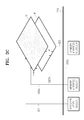
- FIG. 1A is a diagram illustrating a multi-layered memory device according to an example embodiment.
- a memory unit 12 may include a plurality of memory layers a1 through an formed on a surface of an active circuit unit 11.
- the active circuit unit 11 and the memory unit 12 formed on the surface of the active circuit unit 11 may constitute an example embodiment of a multi-layered memory device.
- the number of memory layers a1 through a n capable of being formed on the active circuit 11 is unlimited.
- the active circuit unit 11 may include a decoder.
- the decoder may further include a row decoder (RD) and a column decoder (CD).
- RD row decoder
- CD column decoder
- Each of the plurality of memorylayers a1 through a n may be formed to have an array structure including a plurality of memory cells.
- each of the plurality of memory layers a1 through a n may be a cross-point type memory array structure.
- an information storage unit 103 and a switch structure 104 e.g., a diode, transistor or the like
- the plurality of first electrode lines 101 and the plurality of second electrode lines 102 may be formed perpendicular or substantially perpendicular to one another.
- the information storage unit 103 may have a memory structure having various forms.
- the information storage unit 103 may be formed of a ferroelectric capacitor, a magnetoresistive element, a phase-change element, a variable-resistance element, an antifuse, and the like, which are memory elements in a reversible structure or an irreversible structure.
- adjacent memory layers from among the plurality of memory layers a1 through a n may be formed to share an electrode, and be stacked.
- Each of the plurality of memory layers a1 through a n may include a memory array.
- FIG. 1C illustrates an example embodiment of a memory array 120.
- FIG. 1D illustrates another example embodiment of a memory array including a plurality of sub-arrays 121.
- Each of the plurality of memory layers a1 through a n may include a memory array such as the memory arrays shown in FIGS. 1C and 1D .
- Each of the example embodiments shown in FIGS. 1C and 1D may be used in conjunction with one another or separate.
- memory layer a1 may be configured as shown in FIG. 1C
- memory layer a2 may be configured as shown in FIG. 1D .
- each of the memory layers a1 through a n may be configured as shown in FIG. 1C .
- each of the memory layers a1 through a n may be configured as shown in FIG. 1D .
- FIGS. 2A and 2B are diagrams illustrating a multi-layered memory device according to another example embodiment.
- FIGS. 2A and 2B illustrate a structure in which a memory group including an active circuit unit and a memory unit are stacked sequentially.
- the memory device may include a plurality of memory groups stacked on one another (e.g., vertically stacked). Each of the plurality of memory groups may include an active circuit and a memory unit. Each memory unit may include one or more memory layers.
- a first memory group may include a first active circuit unit 21 and a first memory unit 22.
- the first memory unit 22 may include a plurality of memory layers and may be arranged above (or on) the first active circuit 21.
- the first memory group may beformed on a logic circuit or unit 20.
- the logic unit 20 may also serve as an active circuit.
- a second memory group may include a second active circuit 23 and a memory unit 24 arranged above or on a surface of the second active circuit 23.
- the second memory group may be stacked on the first memory group.
- a third memory group may include a third active circuit 25 and a third memory unit 26 arranged above or on a surface of the third active circuit 25.
- the third memory group may be arranged on the second memory group.
- each of memory units 22, 24, and 26 may be formed on each of active circuit units 21, 23, and 25, respectively.
- the logic unit 20 may include a logic circuit, and may select one or more of the active circuit units 21, 23, and 25.
- Each of the active circuit units 21, 23, and 25 may include a decoder, and may select one or more of the memory units 22, 24, and 26.
- the decoder may include a row decoder (RD) and a column decoder (CD).
- Multi-layered memory devices may include a plurality of the active circuit units 21, 23, and 25 capable of selecting one or more memory units 22, 24, 26 and capable of recording and reproducing information.
- the multi-layered memory devices may further include the logic unit 20 controlling the active circuit units 21, 23, and 25.
- Conventional memory devices have a structure in which an active circuit unit is formed on a silicon substrate and a plurality of memory layers are formed on the active circuit unit.
- the active circuit unit is designed to be a single unit such that many via holes are necessary and a complicated line process is required.
- the multi-layered memory device groups a plurality of memory layers and an active circuit unit controlling the plurality of memory layers into a memory group, and a plurality of the memory groups are stacked each other, thus, there is no limit in the number of memory units, which may be stacked.
- the memory device may include a plurality of memory groups, each including an active circuit and a memory unit.
- Each memory unit may include a plurality of memory layers.
- the plurality of memory groups may be stackedon a logic circuit or unit.
- a first memory unit 201 may be formed on a logic unit 200.
- a first active circuit unit 202 may be formed on the first memory unit 201.
- the first memory unit 201 and the first active circuit 202 constitute a first memory group.
- a second memory unit 203 and a second active circuit unit 204 may be formed on the first active circuit unit 202.
- the second memory unit 203 and the second active circuit 204 constitute a second memory group.
- a third memory unit 205 and a second active circuit unit 206 may be formed on the second active circuit unit 204.
- the third memory unit 205 and the third active circuit 206 constitute a third memory group.
- active circuit units 202, 204, and 206 may be formed on memory units 201, 203, and 205, respectively, and a memory group including a memory unit and an active circuit unit may be sequentially stacked on the logic unit 200.
- the logic unit 200 may include a logic circuit, and may select one or more of the active circuit units 202, 204, and 206.
- Each of the active drcuit units 202, 204, and 206 may include a decoder, and may select one or more of the memory units 201, 203, and 205.
- the decoder may include a row decoder (RD) and a column decoder (CD).
- FIGS. 2C and 2D are diagrams for describing a driving principle of a multi-layered memory device according to example embodiments.
- the multi-layered memory device may have a structure in which a plurality of memory units M and a plurality of active circuit units D are formed on a logic unit 210 (e.g., as shown in FIGS. 2A or 2B ).
- the logic unit 210 may be connected to the plurality of active circuit units D through decoder selection lines 221, and may select a specific active circuit unit from among the plurality of active circuit units D.
- An address (a row and a column) of a desired memory cell may be input through a memory address selection line connected to the logic unit 210 and the plurality of active circuit units D.
- a memory address selection signal may be input through a row line 222a and a column line 222b.
- a specific memory layer of the plurality of memory units M may be selected through a memory level decoder. This will be described in detail below with reference to FIG. 2D .
- a plurality of memory units 211 and 213, and a plurality of active circuit units 212 and 214 may be formed on the logic unit 210.
- the first active circuit unit 212 may write and read data to and from the first memory unit 211.
- the second active circuit unit 214 may write and read data to and from the second memory unit 213.
- G When an active circuit unit and a memory unit are grouped into memory groups denoted by G in FIG. 2D , a plurality of (e.g., an unlimited number of) memory groups G may be formed on the second active circuit unit 214.
- the logic unit 210 may be connected to each of the active circuit units 212 and 214 through the decoder selection lines 221.
- the logic unit 210 may select a specific active circuit unit from among the active circuit units 212 and 214, through the decoder selection lines 221. For example, in the case where the first active circuit unit 212 is selected, a selection line s1 may be ON, whereas the rest of the decoder selection lines 221 may be OFF. Subsequently, an address (a row and a column) of a desired memory cell may be input through a memory selection line 222 connected to the logic unit 210 and the plurality of active circuit units 212 and 214.
- Only the first active circuit unit 212 may be in an ON-state, and thus, only an address of specific memory cells in each of memory layers of the first memory unit 211 may be input. Afterward only a specific memory layer of the first memory unit 211 may be selected through the memory level decoder. As a result, the desired memory cell may be selected.
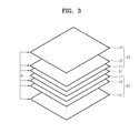
- FIG. 3 is a diagram illustrating a multi-layered memory device according to another example embodiment.
- a memory unit may be formed on each of a plurality of sides of an active circuit.
- memory units 32 and 33 may be formed on top and bottom (e.g., both) surfaces of an active circuit unit 31.
- the first memory unit 32 may include one or more (e.g., a plurality of) memory layers b1 through bn.
- the second memory unit 33 may include one or more (e.g., a plurality of) memory layers c1 through c n . There is no limit in the number of memory layers capable of being included in the memory units 32 and 33.
- the active circuit unit 31 may include a decoder capable of selecting one or more memory layers b1 through bn of memory unit 32 and/or one or more of memory layers c1 through c n of memory unit 33.
- the active circuit 31 may include a sense amplifier, a buffer, a step-down circuit, a boosting circuit, a detecting circuit, and/or a reference voltage circuit.
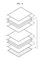
- FIG. 4 is a diagram illustrating a multi-layered memory device according to another example embodiment.
- FIG. 4 illustrates a structure in which a plurality of the memory groups, each of which includes an active circuit unit and one or more memory units formed on both (e.g., opposite) surfaces of the active circuit unit, may be stacked on one another.
- a first memory group may be arranged on a logic circuit 40.
- the first memory group may include a first active circuit unit 42 and a second memory unit 43 formed on opposite surfaces of a first memory unit 41.
- a second memory group may be formed above the first memory group.
- the second memory group may include a third memory unit 44 and a fourth memory unit 45 formed on opposite surfaces of a second active circuit unit 45.
- the logic unit 40 may include a logic circuit, and may select one or more of the active circuit units42 and 45.
- Each of the active circuit units 42 and 45 may include a decoder.
- the active circuit unit 42 may select one or more of the memory units 41 and 43 formed on surfaces of the active circuit unit 42.
- the active circuit unit 45 may select one or more of the memory units 44 and 46 formed on surfaces of the active circuit unit 45.
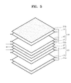
- FIG. 5 is a diagram illustrating a multi-layered memory device according to another example embodiment.
- a column decoder (CD) and a row decoder (RD) may be formed on separate layers so as to select a memory unit.
- a first memory unit 53 may be formed on a first active circuit unit 51 a.
- a second active circuit unit 52a, a second memory unit 54, and a third active circuit unit 51 b may be formed on the first memory unit 53.
- the first active circuit unit 51 a and the third active circuit unit 51 b may include one of the CD and the RD. If the first active circuit unit 51a and the third active circuit unit 51b include the CD, the second active circuit unit 52a may include the RD. Alternatively, if the first and third active circuit units 51 a and 51 b include the RD, then the second active circuit 52a may include the CD.
- the first memory unit 53 may include one or more memory layers d1 through dn
- the second memory unit 54 may include one or more memory layers e1 through en. There is no limit in the number of memory layers capable of being formed on the active circuit units.
- Each of the active circuit units 51a, 52a,and 51b may be connected to one or more of the first and second memory units 53 and 54 in upper and lower directions so as to select the one or more memory layers d1 through dn of the first memory unit 53 or the one or more memory layers e1 through en of the second memory unit 54.
- the first and second active circuit units 51 a and 52a may be used to select the one or more memory layers d1 through dn of the first memory unit 53.
- the third active circuit unit 51 b includes the CD and the second active circuit unit 52a includes the RD, the second and third active circuit units 52a and 51 b may be used to select the one or more memory layers e1 through en of the second memory unit 53
- FIG. 6 is a diagram illustrating a multi-layered memory device according to another example embodiment.
- a first active circuit unit 61 and a first memory unit 64 may be formed on a logic unit 60.
- a second active circuit unit 62 and a second memory unit 65 may be formed on the first memory unit 64.
- a third active circuit unit 63 and a third memory unit 66 may be formed above the second memory unit 65.
- the logic unit 60 may include a logic circuit, and may select one or more of the active circuit units 61, 62, and 63.
- Each of the active circuit units 61, 62, and 63 may include one of a CD and a RD, and may respectively select one or more of the memory units 64, 65, and 66.
- the first memory unit 64 may be formed on a second surface of the active circuit unit 61 and on a first surface of the second active circuit 62.
- the second memory unit 65 may be formed on a second surface of the second active circuit unit 62 and a first surface of the third active circuit unit 63.
- the third memory unit 66 may be formed on a second surface of the third active circuit unit 63.
- each of the active circuit units 61, 62, and 63 may include both the CD and the RD.
- the CD of the first active circuit unit 61 and the RD of the second active circuit unit 62 may be used to address the first memory unit 64.
- the CD of the second active circuit unit 62 and the RD of the third active circuit unit 63 may be used to address the second memory unit 65.
- the RD of the first active circuit unit 61 and the CD of the second active circuit unit 62 may be used to address the first memory unit 64
- the RD of the second active circuit unit 62 and the CD of the third active circuit unit 63 may be used to address the second memory unit 65.
- memory layers of the multi-layered memory device may be formed as a cross-point type memory array.
- a plurality of lower electrode lines and a plurality of upper electrode lines crossing the plurality of lower electrode lines may be formed in each of the memory layers, and a switch structure and an electric charge storage structure may be sequentially formed in an area where the plurality of lower and upper electrode lines cross each other.
- the plurality of lower electrode lines and the plurality of upper electrode lines may be individually connected to the RD or the CD of the active circuit unit.
- the logic unit 60 may be formed on a silicon substrate or a non-silicon substrate.
- an interlayer dielectrics (ILD) process may be performed.
- the memory unit and the active circuit unit may then be formed repeatedly on the logic unit 60.
- the non-silicon substrate are a plastic substrate, a glass substrate, a ceramic substrate, an oxide substrate, or a nitride substrate.
- the active circuit unit may include a decoder, and optionally, a sense amplifier, a buffer, a step-down circuit, a boosting circuit, a detecting circuit, and/or a reference voltage circuit.
- the active circuit unit is formed on the silicon substrate such that an area is limited, a processable memory cell area is also limited, and the number of stackable memory layers is limited.
- the active circuit unit may be formed between each of memory units so that such limits may be overcome.
- FIGS. 7A and 7B are diagrams illustrating an array structure of a decoder circuit of an active circuit unit in a structure in which a memory unit is formed on one surface of the active circuit unit of a multi-layered memory device according to another example embodiment.
- Each decoder circuit may include a RD and a CD.
- a RD and a CD may be formed on an active circuit unit 71.
- Row address lines r extending upward from the RD connect the active circuit unit 71 to a memory unit 72 arranged above the active circuit unit 71 through vias V.
- Column address lines c extending upward from the CD also connect the active circuit unit 71 to the memory unit 72 through vias V. If the memory unit 72 includes one or more memory layers, the row address lines r and the column address lines c may be connected to each of the one or more memory layers.
- an active circuit unit 701 may include a RD and a CD.
- Row address lines r extending downward from the RD connect the active circuit unit 701 to a memory unit 702 arranged below the active circuit unit 701 through vias V.
- Column address lines c extending downward from the CD also connect the active circuit unit 701 to the memory unit 702 through vias V. If the memory unit 702 includes one or more memory layers, the row address lines r and the column address lines c may be connected to each of the one or more memory layers.
- the row address lines r and the column address lines c may be connected to each of the plurality of memory layers.
- FIGS. 8A and 8B are diagrams illustrating a structure of a multi-layered memory device in which one of a RD circuit and a CD circuit is formed below a memory unit, and the other one of the RD circuit and the CD circuit is formed above the memory unit, such that information is recorded in and read from multi-layered memory devices according to example embodiments.
- a memory unit 82 and a second active circuit unit 83 may be sequentially formed on a first active circuit unit 81.
- a CD may be formed on the first active circuit unit 81, and a RD may be formed on the second active circuit unit 83.
- Column address lines c extending upward from the CD of the first active circuit unit 81 may be connected to the memory unit 82 through vias V.
- the CD of the first active circuit unit 81 may be connected to memory unit 82 in an alternating manner such that adjacent columns of the memory array are connected to different sides of the CD.
- a first of two adjacent columns may be connected to a via V at a first side of the first active circuit unit 81, whereas a second of two adjacent columns of the memory unit 82 may be connected to a second, opposite side of the CD.
- Row address lines r extending downward from the RD of the second active circuit unit 83 may be connected to the memory unit 82 through vias V.
- the RD of the second active circuit unit 83 may be connected to memory unit 82 in an alternating manner such that adjacent rows of the memory array are connected to different sides of the RD.
- a first of two adjacent rows may be connected to a via V at a first side of the second active circuit unit 83, whereas a second of two adjacent rows of the memory unit 82 may be connected to a second, opposite side of the second active circuit unit 83.
- the first and second side to which the row address lines r are connected may be different from the first and second sides that the column address lines c are connected.
- the row address lines r and the column address lines c may be connected to each of the plurality of memory layers.
- column address lines c extending upward from a CD of a first active circuit unit 801 may be connected to a memory unit 802 through vias V on only one side end of the first active circuit unit 801.
- Row address lines r extending from a RD of a second active circuit unit 803 may be connected to the memory unit 802 through vias V at only a front end of the second active circuit unit 803. If the memory unit 802 includes a plurality of memory layers, the row address lines r and the column address lines c may be connected to each of the plurality of memory layers.
- FIGS. 9A and 9B are diagrams illustrating a structure of a multi-layered memory device in which vias V are formed alternately to increase density of address lines extending from a CD and a RD in the multi-layered memory device according to another example embodiment.
- a RD and a CD may be formed on ends of respective first and second sides of an active circuit unit 91.
- a memory unit 92 may be formed below the active circuit unit 91.
- Row address lines r and column address lines c extending from the RD and the CD, respectively, of the active circuit unit 91, may be connected to the memory unit 92 through vias V.
- the vias V may be formed alternately offset from one another in a given direction.
- the vias V connected to the row address lines r may be offset from one another in a direction that is perpendicular to a direction in which the first side of the active circuit unit 91 extends.
- the vias V connected to the column address lines c may be offset from one another in a direction that is perpendicular to a direction in which the second side of the active circuit unit 91 extends.
- an active circuit unit 901 may include a RD and a CD.
- a CD may be formed on ends of first and second sides of the active circuit unit 901
- the RD may be formed on ends of third and fourth sides of the active circuit unit 901.
- the first and second sides may be opposite to one another, and the third and fourth sides may be opposite to one another.
- a memory unit 902 may be formed below the active circuit unit 901.
- Row address lines r and column address lines c extending from the RD and the CD, respectively, of the active circuit unit 901 may be connected to the memory unit 902 through vias V.
- the vias V may be formed alternately offset from one another in a given direction.
- the vias V connected to the row address lines r may be offset from one another in a direction that is perpendicular to a direction in which the first and second sides of the active circuit unit 901 extends.
- the vias V connected to the column address lines c may be offset from one another in a direction that is perpendicular to a direction in which the third and fourth sides of the active circuit unit 901 extends.
- the position and shape of vias Via V may be selectively determined according to configuration and/or density of an array device of the memory units 92 and 902, but example embodiments are not limited thereto.
- the active circuit unit and the memory unit illustrated in each of FIGS. 7A through 9B may be grouped into a memory group, and the memory group may be stacked repeatedly.
- connection lines may be simplified to reduce the number of vias as compared to a conventional memory device using only a single active circuit unit.
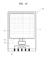
- FIG. 10 is a diagram illustrating a multi-layered memory device according to another example embodiment.
- the multi-layered memory device 100 may include a memory area 102 formed on a substrate 101, an input/output (I/O) chip 104, a parallel bus line 103 connecting the memory area 102 and the I/O chip 104, and a serial bus line 105 connecting the I/O chip 104 and a master device or module (not shown).
- the memory area 102 may have a multi-layered structure, for example, as discussed above.
- Multi-layered memory devices may be used as, for example, media devices for various products, such as, mobile or cellular phones, smart phones, personal digital assistants (PDAs), laptop or desktop computers, digital cameras, digital camcorders, MP3 or other portable music player, etc.
- PDAs personal digital assistants
- laptop or desktop computers digital cameras
- digital camcorders digital camcorders
- MP3 or other portable music player etc.
Landscapes
- Engineering & Computer Science (AREA)
- Computer Hardware Design (AREA)
- Semiconductor Memories (AREA)
- Read Only Memory (AREA)
- Dram (AREA)
Applications Claiming Priority (2)
| Application Number | Priority Date | Filing Date | Title |
|---|---|---|---|
| KR20070092651 | 2007-09-12 | ||
| KR1020080047092A KR100935936B1 (ko) | 2007-09-12 | 2008-05-21 | 적층 메모리 장치 |
Publications (2)
| Publication Number | Publication Date |
|---|---|
| EP2037461A2 true EP2037461A2 (de) | 2009-03-18 |
| EP2037461A3 EP2037461A3 (de) | 2009-10-28 |
Family
ID=39884760
Family Applications (1)
| Application Number | Title | Priority Date | Filing Date |
|---|---|---|---|
| EP08164176A Withdrawn EP2037461A3 (de) | 2007-09-12 | 2008-09-11 | Mehrschichtige Speichervorrichtungen |
Country Status (3)
| Country | Link |
|---|---|
| US (3) | US7898893B2 (de) |
| EP (1) | EP2037461A3 (de) |
| JP (1) | JP2009071313A (de) |
Cited By (6)
| Publication number | Priority date | Publication date | Assignee | Title |
|---|---|---|---|---|
| EP2175453A1 (de) | 2008-10-10 | 2010-04-14 | Samsung Electronics Co., Ltd. | Gestapelte Speichervorrichtung und Verfahren dafür |
| EP2234112A1 (de) | 2009-03-25 | 2010-09-29 | Samsung Electronics Co., Ltd. | Gestapelte Speichervorrichtungen mit hierarchischer Dekodierungs-Struktur |
| EP2249348A3 (de) * | 2009-05-04 | 2011-01-19 | Samsung Electronics Co., Ltd. | Gestapelte Speichervorrichtungen |
| JP2015207761A (ja) * | 2014-04-11 | 2015-11-19 | 株式会社半導体エネルギー研究所 | 半導体装置及び電子機器 |
| US11968820B2 (en) | 2019-02-22 | 2024-04-23 | Semiconductor Energy Laboratory Co., Ltd. | Semiconductor device and electronic device including the semiconductor device |
| US12069846B2 (en) | 2019-01-29 | 2024-08-20 | Semiconductor Energy Laboratory Co., Ltd. | Memory device |
Families Citing this family (17)
| Publication number | Priority date | Publication date | Assignee | Title |
|---|---|---|---|---|
| US7990762B2 (en) * | 2008-02-06 | 2011-08-02 | Unity Semiconductor Corporation | Integrated circuits to control access to multiple layers of memory |
| US8254191B2 (en) | 2008-10-30 | 2012-08-28 | Micron Technology, Inc. | Switched interface stacked-die memory architecture |
| TWI492432B (zh) * | 2009-12-17 | 2015-07-11 | Hitachi Ltd | Semiconductor memory device and manufacturing method thereof |
| JP5289353B2 (ja) * | 2010-02-05 | 2013-09-11 | 株式会社東芝 | 半導体記憶装置 |
| TW201207852A (en) * | 2010-04-05 | 2012-02-16 | Mosaid Technologies Inc | Semiconductor memory device having a three-dimensional structure |
| KR20110135299A (ko) * | 2010-06-10 | 2011-12-16 | 삼성전자주식회사 | 반도체 메모리 장치 |
| CN104380382A (zh) | 2012-03-26 | 2015-02-25 | 英特尔公司 | 三维存储器控制电路 |
| US20150287706A1 (en) * | 2012-10-24 | 2015-10-08 | Mitsunari Sukekawa | Semiconductor device and method for manufacturing the same |
| US9875789B2 (en) * | 2013-11-22 | 2018-01-23 | Taiwan Semiconductor Manufacturing Company, Ltd. | 3D structure for advanced SRAM design to avoid half-selected issue |
| US9558791B2 (en) * | 2013-12-05 | 2017-01-31 | Taiwan Semiconductor Manufacturing Company Limited | Three-dimensional static random access memory device structures |
| WO2017126014A1 (ja) | 2016-01-18 | 2017-07-27 | ウルトラメモリ株式会社 | 積層型半導体装置及びその製造方法 |
| JP7391874B2 (ja) * | 2018-11-08 | 2023-12-05 | 株式会社半導体エネルギー研究所 | 半導体装置 |
| WO2020136464A1 (ja) * | 2018-12-28 | 2020-07-02 | 株式会社半導体エネルギー研究所 | メモリデバイス、当該メモリデバイスを有する半導体装置 |
| CN114258586A (zh) | 2019-08-22 | 2022-03-29 | 株式会社半导体能源研究所 | 存储单元及存储装置 |
| CN113257296B (zh) * | 2021-05-11 | 2025-06-24 | 北京灵汐科技有限公司 | 存储阵列 |
| US11974422B2 (en) * | 2021-11-04 | 2024-04-30 | Taiwan Semiconductor Manufacturing Company, Ltd. | Semiconductor device |
| CN116741227B (zh) * | 2023-08-09 | 2023-11-17 | 浙江力积存储科技有限公司 | 一种三维存储器架构及其操作方法和存储器 |
Citations (2)
| Publication number | Priority date | Publication date | Assignee | Title |
|---|---|---|---|---|
| EP0387834A2 (de) * | 1989-03-14 | 1990-09-19 | Kabushiki Kaisha Toshiba | Halbleiterstruktur zur Datenverarbeitung und -speicherung |
| KR20010088672A (ko) * | 2001-08-20 | 2001-09-28 | 심재택 | 반도체 적층 구조 및 이를 이용한 반도체 |
Family Cites Families (23)
| Publication number | Priority date | Publication date | Assignee | Title |
|---|---|---|---|---|
| JPH0372664A (ja) | 1989-08-11 | 1991-03-27 | Olympus Optical Co Ltd | 光入力型三次元集積メモリ |
| JPH05102430A (ja) * | 1991-04-23 | 1993-04-23 | Mitsubishi Electric Corp | 半導体装置およびその製造方法 |
| US5561622A (en) * | 1993-09-13 | 1996-10-01 | International Business Machines Corporation | Integrated memory cube structure |
| JPH06208796A (ja) * | 1993-11-01 | 1994-07-26 | Hitachi Ltd | 半導体メモリ |
| US5687108A (en) * | 1996-04-10 | 1997-11-11 | Proebsting; Robert J. | Power bussing layout for memory circuits |
| US5835396A (en) * | 1996-10-17 | 1998-11-10 | Zhang; Guobiao | Three-dimensional read-only memory |
| US5915167A (en) | 1997-04-04 | 1999-06-22 | Elm Technology Corporation | Three dimensional structure memory |
| NO308149B1 (no) * | 1998-06-02 | 2000-07-31 | Thin Film Electronics Asa | Skalerbar, integrert databehandlingsinnretning |
| US6185121B1 (en) * | 1998-02-26 | 2001-02-06 | Lucent Technologies Inc. | Access structure for high density read only memory |
| US5991224A (en) | 1998-05-22 | 1999-11-23 | International Business Machines Corporation | Global wire management apparatus and method for a multiple-port random access memory |
| US6034882A (en) | 1998-11-16 | 2000-03-07 | Matrix Semiconductor, Inc. | Vertically stacked field programmable nonvolatile memory and method of fabrication |
| WO2000038234A1 (en) * | 1998-12-04 | 2000-06-29 | Thin Film Electronics Asa | Scalable data processing apparatus |
| JP2002251884A (ja) | 2001-02-21 | 2002-09-06 | Toshiba Corp | 半導体記憶装置及びそのシステム装置 |
| EP1408508A1 (de) * | 2001-07-17 | 2004-04-14 | Mitsubishi Denki Kabushiki Kaisha | Speicherbaustein |
| US6504742B1 (en) | 2001-10-31 | 2003-01-07 | Hewlett-Packard Company | 3-D memory device for large storage capacity |
| JP4419049B2 (ja) | 2003-04-21 | 2010-02-24 | エルピーダメモリ株式会社 | メモリモジュール及びメモリシステム |
| US7327600B2 (en) * | 2004-12-23 | 2008-02-05 | Unity Semiconductor Corporation | Storage controller for multiple configurations of vertical memory |
| US20070132049A1 (en) * | 2005-12-12 | 2007-06-14 | Stipe Barry C | Unipolar resistance random access memory (RRAM) device and vertically stacked architecture |
| TW200802369A (en) * | 2005-12-30 | 2008-01-01 | Hynix Semiconductor Inc | Nonvolatile semiconductor memory device |
| US20070253245A1 (en) * | 2006-04-27 | 2007-11-01 | Yadav Technology | High Capacity Low Cost Multi-Stacked Cross-Line Magnetic Memory |
| US7619945B2 (en) * | 2006-08-18 | 2009-11-17 | Unity Semiconductor Corporation | Memory power management |
| KR100819005B1 (ko) * | 2007-02-16 | 2008-04-03 | 삼성전자주식회사 | 저항체를 이용한 비휘발성 메모리 장치 |
| US7996600B2 (en) * | 2007-08-30 | 2011-08-09 | Unity Semiconductor Corporation | Memory emulation in an electronic organizer |
-
2008
- 2008-09-11 US US12/232,146 patent/US7898893B2/en active Active
- 2008-09-11 EP EP08164176A patent/EP2037461A3/de not_active Withdrawn
- 2008-09-12 JP JP2008235606A patent/JP2009071313A/ja active Pending
-
2011
- 2011-01-19 US US12/929,354 patent/US8514653B2/en active Active
- 2011-01-19 US US12/929,355 patent/US8526263B2/en active Active
Patent Citations (2)
| Publication number | Priority date | Publication date | Assignee | Title |
|---|---|---|---|---|
| EP0387834A2 (de) * | 1989-03-14 | 1990-09-19 | Kabushiki Kaisha Toshiba | Halbleiterstruktur zur Datenverarbeitung und -speicherung |
| KR20010088672A (ko) * | 2001-08-20 | 2001-09-28 | 심재택 | 반도체 적층 구조 및 이를 이용한 반도체 |
Cited By (11)
| Publication number | Priority date | Publication date | Assignee | Title |
|---|---|---|---|---|
| EP2175453A1 (de) | 2008-10-10 | 2010-04-14 | Samsung Electronics Co., Ltd. | Gestapelte Speichervorrichtung und Verfahren dafür |
| US8547719B2 (en) | 2008-10-10 | 2013-10-01 | Samsung Electronics Co., Ltd. | Stacked memory device and method thereof |
| EP2234112A1 (de) | 2009-03-25 | 2010-09-29 | Samsung Electronics Co., Ltd. | Gestapelte Speichervorrichtungen mit hierarchischer Dekodierungs-Struktur |
| JP2010232653A (ja) * | 2009-03-25 | 2010-10-14 | Samsung Electronics Co Ltd | 積層メモリ素子 |
| US8054665B2 (en) | 2009-03-25 | 2011-11-08 | Samsung Electronics Co., Ltd. | Stacked memory device including a pre-decoder/pre-driver sandwiched between a plurality of inter-decoders/inter-drivers |
| EP2249348A3 (de) * | 2009-05-04 | 2011-01-19 | Samsung Electronics Co., Ltd. | Gestapelte Speichervorrichtungen |
| US8611121B2 (en) | 2009-05-04 | 2013-12-17 | Samsung Electronics Co., Ltd. | Stacked memory devices |
| JP2015207761A (ja) * | 2014-04-11 | 2015-11-19 | 株式会社半導体エネルギー研究所 | 半導体装置及び電子機器 |
| US12069846B2 (en) | 2019-01-29 | 2024-08-20 | Semiconductor Energy Laboratory Co., Ltd. | Memory device |
| US11968820B2 (en) | 2019-02-22 | 2024-04-23 | Semiconductor Energy Laboratory Co., Ltd. | Semiconductor device and electronic device including the semiconductor device |
| US12593432B2 (en) | 2019-02-22 | 2026-03-31 | Semiconductor Energy Laboratory Co., Ltd. | Semiconductor device including layer comprising memory cell |
Also Published As
| Publication number | Publication date |
|---|---|
| US20110116297A1 (en) | 2011-05-19 |
| JP2009071313A (ja) | 2009-04-02 |
| US8526263B2 (en) | 2013-09-03 |
| US20090086525A1 (en) | 2009-04-02 |
| US20110116336A1 (en) | 2011-05-19 |
| US8514653B2 (en) | 2013-08-20 |
| EP2037461A3 (de) | 2009-10-28 |
| US7898893B2 (en) | 2011-03-01 |
Similar Documents
| Publication | Publication Date | Title |
|---|---|---|
| US7898893B2 (en) | Multi-layered memory devices | |
| CN101388236B (zh) | 多层存储装置 | |
| CN102150267B (zh) | 用于制造3d存储器阵列的共享x-线掩模和共享y-线掩模 | |
| US6687147B2 (en) | Cubic memory array with diagonal select lines | |
| CN101939838B (zh) | 多个存储器单元和方法 | |
| JP5016151B2 (ja) | 抵抗変化型不揮発性記憶装置 | |
| US8243493B2 (en) | Resistance change memory device | |
| US7986545B2 (en) | Non-volatile memory device and method of operating the same | |
| US11469214B2 (en) | Stacked architecture for three-dimensional NAND | |
| EP2234112B1 (de) | Gestapelte Speichervorrichtungen mit hierarchischer Dekodierungs-Struktur | |
| JP2003209222A (ja) | 大記憶容量のための3−dメモリ素子 | |
| CN103069496A (zh) | 用于控制三维存储器元件阵列的单器件驱动器电路 | |
| JP2009004725A (ja) | 抵抗変化型不揮発性記憶装置 | |
| US8295070B2 (en) | Resistance change memory | |
| US9336877B2 (en) | Nonvolatile memory device using variable resistive element | |
| CN112119462A (zh) | 2叠层3d pcm存储器的分布式阵列和cmos架构的编程和读取偏置方案 | |
| JP2007242735A (ja) | 不揮発性半導体記憶装置 | |
| US8089797B2 (en) | Information storage devices including vertical nano wires | |
| US20110026301A1 (en) | Semiconductor memory device | |
| EP4567797A1 (de) | 3d dram mit bitleitungsauswahl- und vorladetransistoren | |
| US7139183B2 (en) | Logical arrangement of memory arrays | |
| CN100431040C (zh) | 存储器电路 | |
| WO2026065684A1 (zh) | 一种存储器及其访问控制方法、电子设备 | |
| CN119451132A (zh) | 高速三维存储器及系统 | |
| WO2024174309A1 (zh) | 熔丝阵列电路和存储器 |
Legal Events
| Date | Code | Title | Description |
|---|---|---|---|
| PUAI | Public reference made under article 153(3) epc to a published international application that has entered the european phase |
Free format text: ORIGINAL CODE: 0009012 |
|
| AK | Designated contracting states |
Kind code of ref document: A2 Designated state(s): AT BE BG CH CY CZ DE DK EE ES FI FR GB GR HR HU IE IS IT LI LT LU LV MC MT NL NO PL PT RO SE SI SK TR |
|
| AX | Request for extension of the european patent |
Extension state: AL BA MK RS |
|
| PUAL | Search report despatched |
Free format text: ORIGINAL CODE: 0009013 |
|
| AK | Designated contracting states |
Kind code of ref document: A3 Designated state(s): AT BE BG CH CY CZ DE DK EE ES FI FR GB GR HR HU IE IS IT LI LT LU LV MC MT NL NO PL PT RO SE SI SK TR |
|
| AX | Request for extension of the european patent |
Extension state: AL BA MK RS |
|
| 17P | Request for examination filed |
Effective date: 20100203 |
|
| 17Q | First examination report despatched |
Effective date: 20100303 |
|
| AKX | Designation fees paid |
Designated state(s): DE FR GB |
|
| RAP1 | Party data changed (applicant data changed or rights of an application transferred) |
Owner name: SAMSUNG ELECTRONICS CO., LTD. |
|
| STAA | Information on the status of an ep patent application or granted ep patent |
Free format text: STATUS: THE APPLICATION IS DEEMED TO BE WITHDRAWN |
|
| 18D | Application deemed to be withdrawn |
Effective date: 20140212 |