EP2037493A2 - Procédé d'assemblage de balle conductrice et appareil d'assemblage de balle conductrice - Google Patents
Procédé d'assemblage de balle conductrice et appareil d'assemblage de balle conductrice Download PDFInfo
- Publication number
- EP2037493A2 EP2037493A2 EP08161922A EP08161922A EP2037493A2 EP 2037493 A2 EP2037493 A2 EP 2037493A2 EP 08161922 A EP08161922 A EP 08161922A EP 08161922 A EP08161922 A EP 08161922A EP 2037493 A2 EP2037493 A2 EP 2037493A2
- Authority
- EP
- European Patent Office
- Prior art keywords
- mask
- ball
- conductive
- conductive balls
- mounting
- Prior art date
- Legal status (The legal status is an assumption and is not a legal conclusion. Google has not performed a legal analysis and makes no representation as to the accuracy of the status listed.)
- Granted
Links
Images


Classifications
-
- H—ELECTRICITY
- H10—SEMICONDUCTOR DEVICES; ELECTRIC SOLID-STATE DEVICES NOT OTHERWISE PROVIDED FOR
- H10W—GENERIC PACKAGES, INTERCONNECTIONS, CONNECTORS OR OTHER CONSTRUCTIONAL DETAILS OF DEVICES COVERED BY CLASS H10
- H10W70/00—Package substrates; Interposers; Redistribution layers [RDL]
- H10W70/01—Manufacture or treatment
- H10W70/05—Manufacture or treatment of insulating or insulated package substrates, or of interposers, or of redistribution layers
- H10W70/093—Connecting or disconnecting other interconnections thereto or therefrom, e.g. connecting bond wires or bumps
-
- B—PERFORMING OPERATIONS; TRANSPORTING
- B23—MACHINE TOOLS; METAL-WORKING NOT OTHERWISE PROVIDED FOR
- B23K—SOLDERING OR UNSOLDERING; WELDING; CLADDING OR PLATING BY SOLDERING OR WELDING; CUTTING BY APPLYING HEAT LOCALLY, e.g. FLAME CUTTING; WORKING BY LASER BEAM
- B23K3/00—Tools, devices or special appurtenances for soldering, e.g. brazing, or unsoldering, not specially adapted for particular methods
- B23K3/06—Solder feeding devices; Solder melting pans
- B23K3/0607—Solder feeding devices
- B23K3/0623—Solder feeding devices for shaped solder piece feeding, e.g. preforms, bumps, balls, pellets, droplets
-
- H—ELECTRICITY
- H05—ELECTRIC TECHNIQUES NOT OTHERWISE PROVIDED FOR
- H05K—PRINTED CIRCUITS; CASINGS OR CONSTRUCTIONAL DETAILS OF ELECTRIC APPARATUS; MANUFACTURE OF ASSEMBLAGES OF ELECTRICAL COMPONENTS
- H05K3/00—Apparatus or processes for manufacturing printed circuits
- H05K3/30—Assembling printed circuits with electric components, e.g. with resistors
- H05K3/32—Assembling printed circuits with electric components, e.g. with resistors electrically connecting electric components or wires to printed circuits
- H05K3/34—Assembling printed circuits with electric components, e.g. with resistors electrically connecting electric components or wires to printed circuits by soldering
- H05K3/3465—Application of solder
- H05K3/3478—Application of solder preforms; Transferring prefabricated solder patterns
-
- H—ELECTRICITY
- H10—SEMICONDUCTOR DEVICES; ELECTRIC SOLID-STATE DEVICES NOT OTHERWISE PROVIDED FOR
- H10W—GENERIC PACKAGES, INTERCONNECTIONS, CONNECTORS OR OTHER CONSTRUCTIONAL DETAILS OF DEVICES COVERED BY CLASS H10
- H10W72/00—Interconnections or connectors in packages
- H10W72/01—Manufacture or treatment
- H10W72/011—Apparatus therefor
- H10W72/0112—Apparatus for manufacturing bump connectors
-
- B—PERFORMING OPERATIONS; TRANSPORTING
- B23—MACHINE TOOLS; METAL-WORKING NOT OTHERWISE PROVIDED FOR
- B23K—SOLDERING OR UNSOLDERING; WELDING; CLADDING OR PLATING BY SOLDERING OR WELDING; CUTTING BY APPLYING HEAT LOCALLY, e.g. FLAME CUTTING; WORKING BY LASER BEAM
- B23K2101/00—Articles made by soldering, welding or cutting
- B23K2101/36—Electric or electronic devices
- B23K2101/40—Semiconductor devices
-
- H—ELECTRICITY
- H05—ELECTRIC TECHNIQUES NOT OTHERWISE PROVIDED FOR
- H05K—PRINTED CIRCUITS; CASINGS OR CONSTRUCTIONAL DETAILS OF ELECTRIC APPARATUS; MANUFACTURE OF ASSEMBLAGES OF ELECTRICAL COMPONENTS
- H05K2203/00—Indexing scheme relating to apparatus or processes for manufacturing printed circuits covered by H05K3/00
- H05K2203/01—Tools for processing; Objects used during processing
- H05K2203/0104—Tools for processing; Objects used during processing for patterning or coating
- H05K2203/0139—Blade or squeegee, e.g. for screen printing or filling of holes
-
- H—ELECTRICITY
- H05—ELECTRIC TECHNIQUES NOT OTHERWISE PROVIDED FOR
- H05K—PRINTED CIRCUITS; CASINGS OR CONSTRUCTIONAL DETAILS OF ELECTRIC APPARATUS; MANUFACTURE OF ASSEMBLAGES OF ELECTRICAL COMPONENTS
- H05K2203/00—Indexing scheme relating to apparatus or processes for manufacturing printed circuits covered by H05K3/00
- H05K2203/01—Tools for processing; Objects used during processing
- H05K2203/0191—Using tape or non-metallic foil in a process, e.g. during filling of a hole with conductive paste
-
- H—ELECTRICITY
- H05—ELECTRIC TECHNIQUES NOT OTHERWISE PROVIDED FOR
- H05K—PRINTED CIRCUITS; CASINGS OR CONSTRUCTIONAL DETAILS OF ELECTRIC APPARATUS; MANUFACTURE OF ASSEMBLAGES OF ELECTRICAL COMPONENTS
- H05K2203/00—Indexing scheme relating to apparatus or processes for manufacturing printed circuits covered by H05K3/00
- H05K2203/04—Soldering or other types of metallurgic bonding
- H05K2203/041—Solder preforms in the shape of solder balls
-
- H—ELECTRICITY
- H05—ELECTRIC TECHNIQUES NOT OTHERWISE PROVIDED FOR
- H05K—PRINTED CIRCUITS; CASINGS OR CONSTRUCTIONAL DETAILS OF ELECTRIC APPARATUS; MANUFACTURE OF ASSEMBLAGES OF ELECTRICAL COMPONENTS
- H05K2203/00—Indexing scheme relating to apparatus or processes for manufacturing printed circuits covered by H05K3/00
- H05K2203/05—Patterning and lithography; Masks; Details of resist
- H05K2203/0548—Masks
- H05K2203/0557—Non-printed masks
-
- H—ELECTRICITY
- H10—SEMICONDUCTOR DEVICES; ELECTRIC SOLID-STATE DEVICES NOT OTHERWISE PROVIDED FOR
- H10W—GENERIC PACKAGES, INTERCONNECTIONS, CONNECTORS OR OTHER CONSTRUCTIONAL DETAILS OF DEVICES COVERED BY CLASS H10
- H10W72/00—Interconnections or connectors in packages
- H10W72/01—Manufacture or treatment
- H10W72/012—Manufacture or treatment of bump connectors, dummy bumps or thermal bumps
- H10W72/01204—Manufacture or treatment of bump connectors, dummy bumps or thermal bumps using temporary auxiliary members, e.g. using sacrificial coatings or handle substrates
-
- H—ELECTRICITY
- H10—SEMICONDUCTOR DEVICES; ELECTRIC SOLID-STATE DEVICES NOT OTHERWISE PROVIDED FOR
- H10W—GENERIC PACKAGES, INTERCONNECTIONS, CONNECTORS OR OTHER CONSTRUCTIONAL DETAILS OF DEVICES COVERED BY CLASS H10
- H10W72/00—Interconnections or connectors in packages
- H10W72/01—Manufacture or treatment
- H10W72/012—Manufacture or treatment of bump connectors, dummy bumps or thermal bumps
- H10W72/01221—Manufacture or treatment of bump connectors, dummy bumps or thermal bumps using local deposition
- H10W72/01225—Manufacture or treatment of bump connectors, dummy bumps or thermal bumps using local deposition in solid form, e.g. by using a powder or by stud bumping
-
- H—ELECTRICITY
- H10—SEMICONDUCTOR DEVICES; ELECTRIC SOLID-STATE DEVICES NOT OTHERWISE PROVIDED FOR
- H10W—GENERIC PACKAGES, INTERCONNECTIONS, CONNECTORS OR OTHER CONSTRUCTIONAL DETAILS OF DEVICES COVERED BY CLASS H10
- H10W90/00—Package configurations
- H10W90/701—Package configurations characterised by the relative positions of pads or connectors relative to package parts
- H10W90/721—Package configurations characterised by the relative positions of pads or connectors relative to package parts of bump connectors
- H10W90/724—Package configurations characterised by the relative positions of pads or connectors relative to package parts of bump connectors between a chip and a stacked insulating package substrate, interposer or RDL
Definitions
- the present invention relates to a method of mounting a conductive ball and a conductive ball mounting apparatus, more particularly, a method of mounting a conductive ball and a conductive ball mounting apparatus, for mounting a conductive ball on a wiring substrate or the like to form a bump electrode.
- a method of forming a solder ball on a connection pad of a wiring substrate on which a semiconductor chip or the like is to be mounted, and thereby forming a bump electrode In such a method of mounting a solder ball, firstly, as shown in FIG. 1A , a wiring substrate 100 on which solder balls are to be mounted is prepared. In the wiring substrate 100, connection pads 200 are provided on an upper surface of a substrate 110, and a solder resist 300 in which opening portions 300a are provided on the connection pads 200 is formed. Moreover, a flux 400 is coated on the connection pads 200.
- a mask 500 to be used for mounting solder balls is disposed on the wiring substrate 100.
- the mask 500 has a configuration in which a mesh portion 540 is attached to a periphery of a metal mask portion 520, and in which a frame portion 560 is provided on the outer edge of the mesh portion 540. Moreover, opening portions 500a through which solder balls pass are formed in parts of the mask portion 520, the parts corresponding to the connection pads 200 of the wiring substrate 100.
- solder balls 600 are supplied onto the mask 500 and then swept to move to one end side of the mask 500 by a brush 700.
- the solder balls 600 pass through the opening portions 500a of the mask 500 and are arranged to be bonded to the fluxes 400 on the connection pads 200 of the wiring substrate 100.
- the mask 500 is moved upward to be removed from the wiring substrate 100.
- FIG. 2 there is another method using an air supply 750 instead of the use of the brush 700.
- this method by blowing air to the solder balls 600 from an air supply 750 to move the solder balls 600 to one end side of the mask 500, the solder balls 600 is arranged on the connection pads 200 of the wiring substrate 100 while causing the solder balls 600 to pass through the opening portions 500a of the mask 500.
- Patent Literature 1 Japanese Patent Application Publication No. 2004-186286
- a print mask is disposed on a silicon substrate having columnar electrodes, then a large number of solder balls are supplied on the print mask, then air is moderately blown to the solder balls while a squeegee is moved, thereby, solder balls pass through the print mask, and are arranged on the columnar electrodes.
- Patent Literature 2 Japanese Patent Application Publication No. 2006-173195
- a large number of solder balls are supplied on a mask disposed on a wafer, then the solder balls are moved by a filling head provided with a sweep member, to arrange the solder balls in opening portions in the mask, then the solder balls remaining on the mask are swept to the outside of the mask by a removal head provided with a soft squeegee, and are removed consequently.
- solder balls 600 the number of which is considerably larger than that of the opening portions 500a of the mask 500 are supplied on the mask 500. Accordingly, although some of the solder balls 600 pass through the opening portions 500a of the mask 500, some other solder balls 600 remain around the opening portions 500a of the mask 500 in many cases. Such being the case, it is necessary to move the excess solder balls 600 to one end side of the mask 500, or to remove the excess solder balls 600 from the mask 500.
- the excess solder balls 600 remaining on the mask 500 may pass through the opening portions 500a of the mask 500 when the mask 500 is moved upward from the wiring substrate 100 to be separated therefrom, and consequently, multiple solder balls are likely to be mounted on the connection pads 200 of the wiring substrate 100, in some cases.
- the brush In the method in which the excess solder balls on the mask are moved by the brush, the brush needs to be moved repeatedly with many times in order to remove all the excess solder balls. Consequently, a long time is required for the operation, and, hence, the manufacturing efficiency is low. Furthermore, solder balls sometimes adhere to the brush, which is likely to complicate the maintenance.
- the wind pressure needs to be set relatively high in order to efficiently move the solder balls.
- solder balls on the mask sometimes fly to the outside of the mask in some cases.
- the wind pressure is set low enough to prevent solder balls from flying to the outside, it is extremely difficult to move all the excess solder balls.
- a method of mounting a conductive ball which method includes the steps of: disposing a mask on a substrate including connection pads, the mask having opening portions corresponding to the connection pads; supplying conductive balls on the mask; arranging the conductive balls on the connection pad of the substrate through the opening portion of the mask, by moving the conductive balls to one end side of the mask by a ball moving member; and removing excess conductive balls remaining on a region of the mask where the opening portions are provided, by bonding the excess conductive balls to a ball removal film.
- a mask is disposed on a substrate (such as a wiring substrate, or a semiconductor wafer in which semiconductor element is made) having connection pads, the mask having opening portions corresponding to the connection pads. Thereafter, a larger number of conductive balls (solder balls or the like) than that of the opening portions are supplied on the mask.
- the conductive balls are swept and moved to one end side of the mask by moving ball moving member (a brush or the like) in a horizontal direction. Thereby, the conductive balls pass through the opening portions of the mask, and are arranged respectively on the connection pads of the substrate. At this stage, some of the conductive balls remain as excess in regions in which the opening portions are formed, on the mask.
- moving ball moving member a brush or the like
- the excess conductive balls on the mask are bonded to a ball removing film (such as an adhesive film or an electrostatic adsorption film), thereby the excess conductive balls are removed from the mask consequently.
- a ball removing film such as an adhesive film or an electrostatic adsorption film
- this method prevents the excess conductive balls from being mounted on the substrate through the opening portions of the mask when the mask is moved upward to be removed from the substrate. Accordingly, a single conductive ball can be mounted on each of the connection pads of the substrate with high reliability.
- the ball removal film is placed in parallel with the mask in a state that a roll-like film is pulled out. After the conductive balls adhere to the ball removal film and are then removed, a used part of the film is wound, and a new part of the ball removal film is placed on the mask.
- a protrusion portion protruding upward may be provided on an upper surface of the mask. According to this embodiment, even when the ball removal film is displaced closer to the mask, the protrusion portion serves as a stopper, so that the height position of the ball removal film is controlled to be a desired position. Thus, only the excess conductive balls on the mask are selectively removed in a stable manner without removing the conductive balls passing through the opening portions of the mask.
- conductive balls can be mounted on a substrate with high reliability while excess conductive balls on the mask are removed efficiently.
- FIGS. 3 to 9 are cross-sectional views showing a method of mounting a conductive ball, according to a first embodiment of the present invention
- FIGS. 10 to 12 are cross-sectional views showing a method of mounting a semiconductor chip on a wiring substrate on which conductive balls are mounted
- FIG. 13 is a cross-sectional view showing a conductive ball mounting apparatus similarly.
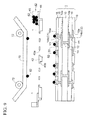
- a wiring substrate 1 on which conductive balls are to be mounted is prepared.
- through holes TH are formed in a core substrate 10 made of glass epoxy resin or the like, and the through holes TH are filled respectively with through-hole electrodes 12 made of copper or the like.
- first wiring layers 14a connected to each other via through-hole electrode 12 and made of copper, are respectively formed on both surfaces of the core substrate 10.
- the first wiring layers 14a which are formed on the both surfaces of the core substrate 10 may be connected to each other with a through-hole plated layer formed on an inner wall of the through holes TH, and the opening in the through holes TH may be filled with resin.
- interlayer insulating films 16 for covering the first wiring layers 14a are formed respectively.
- the interlayer insulating films 16 are formed by affixing resin films made of epoxy, polyimide or the like to the core substrate 10, for example.
- connection pads C1 and C2 are shown as the second wiring layers 14b.
- a solder resist 18 in which an opening portion 18a is provided on each of the connection pads C1, C2 is formed on the second wiring layers 14b on both surfaces of the core substrate 10 respectively.
- fluxes 20 are formed respectively on the connection pads C1 of the second wiring layers 14b on the upper surface of the core substrate 10. The fluxes 20 are coated to be patterned on the connection pads C1 of the second wiring layers 14b by means of printing or a dispenser.
- a rigid substrate is given as an example of the wiring substrate 1.
- a flexible wiring substrate which uses a film as a substrate, may be used as the wiring substrate 1.
- a semiconductor wafer (silicon wafer) on which a semiconductor element (a transistor or the like) and multilayer wiring layers connected to the semiconductor element are formed and connection pads are provided on an uppermost layer, may be used.
- semiconductor wafer is diced after the conductive balls are mounted on the connection pads thereof, thereby an individual semiconductor chip such as a CPU, a memory, or the like is obtained.
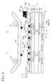
- a conductive ball mounting apparatus 2 for mounting a conductive ball on the connection pad C1 of the second wiring layers 14b on the upper surface of the wiring substrate 1 shown in Fig. 3 will be explained hereunder.
- a conductive ball mounting apparatus 2 includes a stage 30 for placing a substrate 5, and the substrate 5 is fixed on the stage 30 by vacuum contact or the like.
- the conductive ball mounting apparatus 2 also includes a mask 40 having opening portions 40a through which conductive balls pass. The mask 40 is disposed above the substrate 5.
- the mask 40 is composed of a metal mask portion 42 in which opening portions 40a are formed, a mesh portion 44 which is provided on a periphery of the metal mask portion 42, and which is made of resin or the like, and a frame portion 46 which is provided on the outer edge of the mesh portion 44.
- the mask 40 is connected to moving means (not illustrated), and is thereby capable of moving in the vertical directions and horizontal directions with high accuracy.
- the conductive ball mounting apparatus 2 includes ball supply portion 60 for supplying conductive balls 62, and the ball supply portion 60 is disposed above the mask 40.
- the conductive ball mounting apparatus 2 also includes a brush 50 (ball moving member) for sweeping and moving the large number of conductive balls 62 supplied on the mask 40 in the horizontal directions.
- the brush 50 is disposed above the mask 40.
- the brush 50 is connected to moving means (not illustrated), and is thereby capable of moving in the vertical directions and horizontal directions.
- the brush 50 is made to abut to the mask 40, and is then moved in a horizontal direction. Thereby, the conductive balls 62 on the mask 40 are transferred into the opening portions 40a of the mask 40.
- the brush 50 is given as an example of the ball moving member.
- a cylindrical brush may be moved while rotating, or a plate-like squeegee may be employed.
- the ball supply portion 60 and the ball moving member (brush 50) may be integrally provided.
- the conductive ball mounting apparatus 2 of the first embodiment further includes an adhesive film 70 (ball removing film) which removes to bond the excess conductive balls 62 remaining on the mask 40 after the conductive balls 62 are swept into the opening portions 40a of the mask 40.
- the adhesive film 70 is disposed above the mask 40.
- the adhesive film 70 is conveyed by means of a reel-to-reel system. Specifically, a roll-like film wound onto a reel (not illustrated) provided at one end side is pulled out, and is then wound onto a reel (not illustrated) provided at the other end side in a state that the film is pulled to a lower side of the two rollers 72.
- the rollers 72 or the like are connected to moving means (not illustrated), and are thereby capable of moving in the vertical directions and horizontal directions with high accuracy.
- the adhesive film 70 is disposed to be controlled at a predetermined height position from on the mask 40. Also the adhesive film 70 between the two rollers 72 is set to have a size corresponding to that of the area of the mask 40, the area in which the plural opening portions 40a are arranged. The adhesive film 70 is disposed in parallel with the mask 40. Thereafter, the excess conductive balls 62 on the mask 40 are bonded to the adhesive film 70, and the adhesive film 70 is then moved upward. Thereby, the excess conductive balls 62 are removed from the mask 40.
- the adhesive film 70 is wound onto the reel at the other end side, and the rollers 72 rotate. Thereby, the adhesive film 70 on which the conductive balls 62 are boned is moved, so that a new part of adhesive film 70 is placed under the two rollers 72.
- the adhesive film 70 is given as an example of the ball removing film.
- an electrostatic adsorption film which adsorbs the conductive balls 62 thereon by static electricity, may be employed.
- any kind of films can be employed as long as being capable of bonding the conductive balls 62 thereto and removing the conductive balls consequently.
- the conductive ball mounting apparatus 2 also includes an image recognition camera 35 which recognizes an alignment mark provided on the substrate 5, and thus has an alignment function to align such that the opening portions 40a of the mask 40 are disposed respectively above the connection pads of the substrate 5, on the basis of recognizing the alignment mark on the substrate 5.
- the wiring substrate 1 is fixed to be placed on the upper surface of the stage 30 (omitted in FIG. 4 ) of the conductive ball mounting apparatus 2 shown in FIG. 13 .
- the mask 40 having the opening portions 40a described above is disposed on the wiring substrate 1.
- the image recognition camera 35 FIG. 13
- the mask 40 is aligned with the wiring substrate 1 so that the opening portions 40a of the mask 40 can correspond to the connection pads C1 of the wiring substrate 1 respectively.
- a collective recessed portion 40b is provided in the lower portion of the mask 40, the lower portion corresponding to an area where the connection pads C1 of the wiring substrate 1 are arranged with an area array type. Thereby the mask 40 is prevented from coming in contact with the fluxes 20 on the connection pads C1 of the wiring substrate 1.
- the conductive balls 62 are supplied on the mask 40 from the ball supply portion 60.
- the number of the supplied conductive balls 62 is considerably larger than that of the opening portions 40a (corresponding to the connection pads C1 of the wiring substrate 1) of the mask 40.
- a mode in which a semiconductor chip is flip-chip connected to the connection pads C1 of the wiring substrate 1 is illustrated.
- the conductive balls 62 solder balls entirely made of solder, balls composed of a core ball and a solder layer covering the outer surface of the core ball, or balls composed of a core ball made of copper and a solder layer covering the outer surface of the core ball, or the like are used.
- the conductive balls made of various conductive materials can be used depending on the usage of the substrate (work) on which conductive balls are mounted.
- the conductive balls 62 are set to have a diameter of 100 ⁇ m or less (the lower limit is 10 ⁇ m or more, for example). That is, the conductive balls 62 having a relatively small diameter, that a handling thereof is difficult in a method in which all conductive balls are mounted collectively by an adsorption tool or the like, are used.
- the large number of conductive balls 62 are moved to be swept to one end side of the mask 40 (outside the product area) by the brush 50 (ball moving member).
- the conductive balls 62 moved by the brush 50 are transferred into the opening portions 40a of the mask 40 by the brush, and are arranged to be bonded respectively to the fluxes 20 on the connection pads C1 below the opening portions 40a.
- the opening portions 40a of the mask 40 are set to have a size slightly larger than that of the conductive balls 62. Accordingly, the conductive balls 62 can easily pass through the opening portions 40a of the mask 40. In this manner, one of the conductive balls 62 is transferred into each of the opening portions 40a of the mask 40 respectively, and is arranged on the connection pad C1 of the wiring substrate 1 below the mask 40.
- the adhesive film 70 placed under the two rollers 72 described above is moved toward the mask 40. Then, as shown in FIG. 7 , the adhesive film 70 is disposed above the mask 40 while controlling the position in an extent that the adhesive film 70 does not come in contact with the mask 40, and the adhesive film 70 is made to abut onto the excess conductive balls 62 remaining on the mask 40. Thereby the excess conductive balls 62 are bonded to the adhesive film 70. Thereafter, as shown in FIG. 8 , the excess conductive balls 62 are removed from the mask 40 by moving the adhesive film 70 on which the conductive balls 62 are bonded upward.
- the conductive ball mounting apparatus 2 is provided with the adhesive film 70 disposed in parallel with the mask 40. Accordingly, although the excess conductive balls remain on the mask 40, the excess conductive balls 62 can be removed by the adhesive film 70 collectively.
- the excess conductive balls 62 can be removed collectively without repeating the movement of the brush 50 until no excess conductive balls 62 remain on the mask 40. Accordingly, the manufacturing efficiency can be remarkably improved. Moreover, unlike a method in which the conductive balls 62 are moved by blowing air, no conductive balls 62 can fly to the outside since the conductive balls are made to bond onto the adhesive film 70.
- the conductive balls 62 which are moved to the one end side of the mask 40 are left thereon as it is, and are used as part of the conductive balls to be mounted on a wiring substrate which is processed next.
- the mask 40 is also moved upward, and is consequently removed from the wiring substrate 1. Then, the adhesive film 70 is wound by the reel (not illustrated) at the other end side, and the rollers 72 are rotated, thereby a new part of adhesive film 70 is placed under the two rollers 72.
- one of the conductive balls 62 is arranged to bond to the flux 20 on each of the connection pads C1 of the wiring substrate 1 with high reliability. It should be noted that conductive balls can be mounted on the connection pads of the above-mentioned semiconductor wafer as well as the wiring substrate 1, by means of the same method.
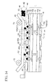
- solder bumps 22 are obtained.
- solder bumps 80a are prepared.
- the solder bumps 80a of the semiconductor chip 80 are placed on the solder bumps 22 of the wiring substrate 1, and they are flip-chip bonding by reflow-heating.
- solder bumps 22 of the wiring substrate 1 and the solder bumps 80a of the semiconductor chip 80 are respectively fused to form bump electrodes 24.
- the semiconductor chip 80 is electrically connected to the connection pads C1 of the wiring substrate 1 via the bump electrodes 24.
- solder balls or the like are mounted on the connection pads C2 on the lower surface of the wiring substrate 1 to form external connection terminals 26.
- the timing at which the external connection terminals 26 are formed may be after the step shown in FIG. 10 (i.e. after the conductive balls 62 are mounted), or may be after the semiconductor chip 80 is mounted.
- a semiconductor device 3 according to the first embodiment is obtained.
- the wiring substrate 1 is divided to be cut, before or after the semiconductor chip 80 is mounted.
- the conductive balls 62 are arranged on the connection pads C1 of the wiring substrate 1 through the opening portions 40a of the mask 40. Thereafter, before the mask 40 is separated upward to be removed from the wiring substrate 1, the excess conductive balls 62 remaining around the opening portions 40 of the mask 40 are bonded to the adhesive film 70, and are removed consequently.
- the conductive balls 62 on the mask 40 are removed by the adhesive film 70 collectively, the conductive balls 62 can be removed more efficiently and stably than a case of employing a method in which the excess conductive balls 62 are moved on the mask 40 by a brush or air.
- the conductive balls 62 can be mounted on the wiring substrate 1 with high reliability.
- FIGS. 14 and 15 are cross-sectional views showing a method of mounting a conductive ball according to a second embodiment of the present invention.
- the same elements as those in the first embodiment are denoted by the same reference numerals, and the detailed description of those elements are omitted.
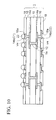
- protrusion portions 48 which protrude upward are provided on the upper surface of the mask 40.
- the protrusion portions 48 serve as stoppers for the adhesive film 70, so that the adhesive film 70 is not placed lower than the upper surfaces of the protrusion portions 48.
- the height of the protrusion portions 48 is set to be lower than the height (diameter) of the conductive balls 62.
- the height of the protrusion portions 48 is set to 20 ⁇ m to 50 ⁇ m.
- the adhesive film 70 can make the excess conductive balls 62 bond by abutting to only the excess conductive balls 62 that should be removed without coming in contact with the metal mask portion 42 of the mask 40.
- the adhesive film 70 is moved upward from the wiring substrate 1, so that the excess conductive balls 62 are removed from the mask 40, as in the first embodiment.
- the protrusion portions 48 for controlling the height position at which the adhesive film 70 is placed are provided on the mask 40, there is no possibility that the adhesive film 70 is displaced toward the mask 40. Accordingly, when the excess conductive balls 62 on the mask 40 are removed by the adhesive film 70, such a situation can be prevented that the conductive balls 62 transferred into the opening portions 40a of the mask 40 are removed simultaneously.
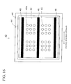
- FIG. 16 shows a state in which the mask 40 provided with the protrusion portions 48 is seen from the above.
- the opening portions 40a of the mask 40 aligned with an area array type are arranged to be divided in four areas.
- the protrusion portions 48 are provided in belt-like shapes (in stripes) so as to partition the groups of opening portions 40a located upside and downside.
- the protrusion portions 48 are each formed in a belt-like shape so as to extend in the same direction as the moving direction of the brush 50. Accordingly, the conductive balls 62 are swept to a longitudinal direction of the protrusion portions 48, and are moved to the one end side of the mask 40. Thus, there is no possibility that the protrusion portions 48 become obstacles when the conductive balls 62 are moved.
- the protrusion portions 48 may be formed integrally with the metal mask portion 42 of the mask 40, or may be formed separately from the mask 40 to be disposed on the mask 40 as spacer parts.
- the second embodiment provides the same effects as those of the first embodiment, and can improve the reliability when the excess conductive balls are removed by the adhesive film, compared to the first embodiment.
Landscapes
- Engineering & Computer Science (AREA)
- Manufacturing & Machinery (AREA)
- Microelectronics & Electronic Packaging (AREA)
- Mechanical Engineering (AREA)
- Electric Connection Of Electric Components To Printed Circuits (AREA)
Applications Claiming Priority (1)
| Application Number | Priority Date | Filing Date | Title |
|---|---|---|---|
| JP2007239045A JP4444322B2 (ja) | 2007-09-14 | 2007-09-14 | 導電性ボールの搭載方法及び導電性ボール搭載装置 |
Publications (3)
| Publication Number | Publication Date |
|---|---|
| EP2037493A2 true EP2037493A2 (fr) | 2009-03-18 |
| EP2037493A3 EP2037493A3 (fr) | 2011-09-14 |
| EP2037493B1 EP2037493B1 (fr) | 2013-11-13 |
Family
ID=40278956
Family Applications (1)
| Application Number | Title | Priority Date | Filing Date |
|---|---|---|---|
| EP08161922.3A Active EP2037493B1 (fr) | 2007-09-14 | 2008-08-06 | Procédé d'assemblage de balle conductrice et appareil d'assemblage de balle conductrice |
Country Status (3)
| Country | Link |
|---|---|
| US (1) | US7854366B2 (fr) |
| EP (1) | EP2037493B1 (fr) |
| JP (1) | JP4444322B2 (fr) |
Families Citing this family (18)
| Publication number | Priority date | Publication date | Assignee | Title |
|---|---|---|---|---|
| JP4828595B2 (ja) * | 2007-12-19 | 2011-11-30 | 新光電気工業株式会社 | 導電性ボール除去方法及び導電性ボール除去装置 |
| JP5181390B2 (ja) * | 2008-06-30 | 2013-04-10 | 澁谷工業株式会社 | ボール搭載装置 |
| JP2010021445A (ja) * | 2008-07-11 | 2010-01-28 | Nippon Steel Materials Co Ltd | 微細ボール除去方法及び除去装置、並びに微細ボール一括搭載方法及び一括搭載装置 |
| US8561880B2 (en) * | 2012-02-11 | 2013-10-22 | International Business Machines Corporation | Forming metal preforms and metal balls |
| US8875978B2 (en) * | 2012-02-11 | 2014-11-04 | International Business Machines Corporation | Forming constant diameter spherical metal balls |
| JP5886120B2 (ja) * | 2012-04-25 | 2016-03-16 | 富士機械製造株式会社 | スキージおよび、スキージを備えた導電性ボール供給装置 |
| US8523046B1 (en) * | 2012-10-18 | 2013-09-03 | International Business Machines Corporation | Forming an array of metal balls or shapes on a substrate |
| KR102029077B1 (ko) | 2013-02-04 | 2019-10-07 | 삼성전자주식회사 | 패키지의 외부접속단자 형성 방법 및 이를 수행하기 위한 장치 |
| JP6109609B2 (ja) * | 2013-03-14 | 2017-04-05 | Aiメカテック株式会社 | ハンダボール印刷機およびハンダボール印刷方法 |
| KR102100867B1 (ko) * | 2013-06-26 | 2020-04-14 | 삼성전자주식회사 | 솔더 볼 탑재 장치 |
| JP6381322B2 (ja) * | 2014-07-07 | 2018-08-29 | マクセルホールディングス株式会社 | 配列用マスク |
| US9905525B1 (en) | 2016-08-18 | 2018-02-27 | Semiconductor Components Industries, Llc | Semiconductor wafer and method of ball drop on thin wafer with edge support ring |
| JP2019206088A (ja) * | 2018-05-28 | 2019-12-05 | 株式会社ボンマーク | ボール配列用マスク及びその製造方法 |
| KR102078935B1 (ko) * | 2018-11-07 | 2020-02-19 | 주식회사 프로텍 | 도전성 볼 탑재 장치 |
| KR102078936B1 (ko) * | 2018-11-07 | 2020-02-19 | 주식회사 프로텍 | 도전성 볼 탑재 방법 |
| CN114531785B (zh) * | 2022-02-21 | 2024-05-14 | 深圳市华星光电半导体显示技术有限公司 | 印锡钢网及印刷锡膏的方法 |
| CN116053149A (zh) * | 2022-12-19 | 2023-05-02 | 海光信息技术股份有限公司 | 一种电子封装方法及电子封装结构 |
| JP7468943B1 (ja) | 2023-01-30 | 2024-04-16 | アスリートFa株式会社 | ボール搭載装置及びボール搭載方法 |
Citations (2)
| Publication number | Priority date | Publication date | Assignee | Title |
|---|---|---|---|---|
| JP2004186286A (ja) | 2002-12-02 | 2004-07-02 | Casio Comput Co Ltd | 金属ボールの形成方法 |
| JP2006173195A (ja) | 2004-12-13 | 2006-06-29 | Athlete Fa Kk | 微小粒子の配置方法および装置 |
Family Cites Families (6)
| Publication number | Priority date | Publication date | Assignee | Title |
|---|---|---|---|---|
| US6191022B1 (en) * | 1999-04-18 | 2001-02-20 | Cts Corporation | Fine pitch solder sphere placement |
| SG99331A1 (en) * | 2000-01-13 | 2003-10-27 | Hitachi Ltd | Method of producing electronic part with bumps and method of producing elctronic part |
| JP2005056901A (ja) * | 2003-08-04 | 2005-03-03 | Nippon Steel Corp | 半導体装置の製造装置及び半導体装置の製造方法 |
| JP2005158944A (ja) * | 2003-11-25 | 2005-06-16 | Renesas Technology Corp | 半導体装置の製造方法 |
| DE102004025279B4 (de) | 2004-05-19 | 2011-04-28 | Infineon Technologies Ag | Anlage für ein Bestücken von Substraten mit Kugelkontakten und Verfahren zum Bestücken von Substraten mit Kugelkontakten |
| WO2007123384A1 (fr) * | 2006-04-25 | 2007-11-01 | Gutierrez Garcia Jose Luis | Outil de lavage à sec de cartes électroniques mal imprimées |
-
2007
- 2007-09-14 JP JP2007239045A patent/JP4444322B2/ja active Active
-
2008
- 2008-08-06 EP EP08161922.3A patent/EP2037493B1/fr active Active
- 2008-08-08 US US12/188,556 patent/US7854366B2/en active Active
Patent Citations (2)
| Publication number | Priority date | Publication date | Assignee | Title |
|---|---|---|---|---|
| JP2004186286A (ja) | 2002-12-02 | 2004-07-02 | Casio Comput Co Ltd | 金属ボールの形成方法 |
| JP2006173195A (ja) | 2004-12-13 | 2006-06-29 | Athlete Fa Kk | 微小粒子の配置方法および装置 |
Also Published As
| Publication number | Publication date |
|---|---|
| EP2037493A3 (fr) | 2011-09-14 |
| JP2009071109A (ja) | 2009-04-02 |
| EP2037493B1 (fr) | 2013-11-13 |
| US20090072011A1 (en) | 2009-03-19 |
| US7854366B2 (en) | 2010-12-21 |
| JP4444322B2 (ja) | 2010-03-31 |
Similar Documents
| Publication | Publication Date | Title |
|---|---|---|
| EP2037493B1 (fr) | Procédé d'assemblage de balle conductrice et appareil d'assemblage de balle conductrice | |
| US8178978B2 (en) | Support mounted electrically interconnected die assembly | |
| JP5014853B2 (ja) | 半導体装置の製造方法 | |
| JP4393538B2 (ja) | 磁性はんだボールの配列装置および配列方法 | |
| US8115300B2 (en) | Wiring substrate and manufacturing method thereof, and semiconductor apparatus | |
| CN100438001C (zh) | 倒装芯片型半导体器件及其制造工艺和电子产品制造工艺 | |
| KR20110103413A (ko) | 전기 전도성 물질의 에어로졸 응용에 의해 형성된 반도체 다이 배선 | |
| US10236242B2 (en) | Chip package and package substrate | |
| US20090130838A1 (en) | Method of forming conductive bumps | |
| US7432114B2 (en) | Semiconductor device manufacturing method | |
| US8141770B2 (en) | Conductive ball mounting method and surplus ball removing apparatus | |
| KR101605610B1 (ko) | 반도체 디바이스의 제조 방법 및 이에 따른 반도체 디바이스 | |
| JP2009188260A (ja) | 半導体装置および実装基板 | |
| JP4206779B2 (ja) | 半導体装置の製造方法 | |
| JP2005026346A (ja) | 半導体チップの積層方法 | |
| KR100652440B1 (ko) | 반도체 패키지, 그 패키지를 이용한 스택 패키지 및 그스택 패키지 형성 방법 | |
| TW201842632A (zh) | 穿透封膠層形成導電路徑之封裝方法 | |
| US20210249373A1 (en) | Semiconductor device and semiconductor device manufacturing method | |
| JP2009147250A (ja) | 導電性ボールの搭載方法及び導電性ボール搭載装置 | |
| JP2009146963A (ja) | 導電性ボールの搭載方法及び導電性ボール搭載装置 | |
| US12087612B2 (en) | Micro device structure and display apparatus | |
| US12191362B2 (en) | Stacked semiconductor devices in sealants and interconnected with pillar electrodes | |
| TW201030935A (en) | Semiconductor die interconnect formed by aerosol application of electrically conductive material | |
| JP2007005832A (ja) | 半導体装置 | |
| JP2007049183A (ja) | 半導体装置 |
Legal Events
| Date | Code | Title | Description |
|---|---|---|---|
| PUAI | Public reference made under article 153(3) epc to a published international application that has entered the european phase |
Free format text: ORIGINAL CODE: 0009012 |
|
| AK | Designated contracting states |
Kind code of ref document: A2 Designated state(s): AT BE BG CH CY CZ DE DK EE ES FI FR GB GR HR HU IE IS IT LI LT LU LV MC MT NL NO PL PT RO SE SI SK TR |
|
| AX | Request for extension of the european patent |
Extension state: AL BA MK RS |
|
| PUAL | Search report despatched |
Free format text: ORIGINAL CODE: 0009013 |
|
| AK | Designated contracting states |
Kind code of ref document: A3 Designated state(s): AT BE BG CH CY CZ DE DK EE ES FI FR GB GR HR HU IE IS IT LI LT LU LV MC MT NL NO PL PT RO SE SI SK TR |
|
| AX | Request for extension of the european patent |
Extension state: AL BA MK RS |
|
| RIC1 | Information provided on ipc code assigned before grant |
Ipc: B23K 3/06 20060101ALI20110811BHEP Ipc: H05K 3/34 20060101ALI20110811BHEP Ipc: H01L 21/48 20060101AFI20110811BHEP |
|
| 17P | Request for examination filed |
Effective date: 20120307 |
|
| AKX | Designation fees paid |
Designated state(s): DE |
|
| RIC1 | Information provided on ipc code assigned before grant |
Ipc: H05K 3/34 20060101ALI20130409BHEP Ipc: H01L 21/48 20060101AFI20130409BHEP Ipc: B23K 3/06 20060101ALI20130409BHEP |
|
| GRAP | Despatch of communication of intention to grant a patent |
Free format text: ORIGINAL CODE: EPIDOSNIGR1 |
|
| INTG | Intention to grant announced |
Effective date: 20130605 |
|
| GRAS | Grant fee paid |
Free format text: ORIGINAL CODE: EPIDOSNIGR3 |
|
| GRAA | (expected) grant |
Free format text: ORIGINAL CODE: 0009210 |
|
| AK | Designated contracting states |
Kind code of ref document: B1 Designated state(s): DE |
|
| REG | Reference to a national code |
Ref country code: DE Ref legal event code: R096 Ref document number: 602008028697 Country of ref document: DE Effective date: 20140109 |
|
| REG | Reference to a national code |
Ref country code: DE Ref legal event code: R097 Ref document number: 602008028697 Country of ref document: DE |
|
| PLBE | No opposition filed within time limit |
Free format text: ORIGINAL CODE: 0009261 |
|
| STAA | Information on the status of an ep patent application or granted ep patent |
Free format text: STATUS: NO OPPOSITION FILED WITHIN TIME LIMIT |
|
| 26N | No opposition filed |
Effective date: 20140814 |
|
| REG | Reference to a national code |
Ref country code: DE Ref legal event code: R097 Ref document number: 602008028697 Country of ref document: DE Effective date: 20140814 |
|
| REG | Reference to a national code |
Ref country code: DE Ref legal event code: R082 Ref document number: 602008028697 Country of ref document: DE Representative=s name: HL KEMPNER PATENTANWAELTE, SOLICITORS (ENGLAND, DE Ref country code: DE Ref legal event code: R082 Ref document number: 602008028697 Country of ref document: DE Representative=s name: HL KEMPNER PATENTANWALT, RECHTSANWALT, SOLICIT, DE Ref country code: DE Ref legal event code: R082 Ref document number: 602008028697 Country of ref document: DE Representative=s name: HL KEMPNER PARTG MBB, DE |
|
| PGFP | Annual fee paid to national office [announced via postgrant information from national office to epo] |
Ref country code: DE Payment date: 20250702 Year of fee payment: 18 |
|
| REG | Reference to a national code |
Ref country code: DE Ref legal event code: R079 Ref document number: 602008028697 Country of ref document: DE Free format text: PREVIOUS MAIN CLASS: H01L0021480000 Ipc: H10W0076010000 |