EP2037530A1 - Circuit RF commutable et séparateur de fréquences pour applications de bande passante de grande portée - Google Patents
Circuit RF commutable et séparateur de fréquences pour applications de bande passante de grande portée Download PDFInfo
- Publication number
- EP2037530A1 EP2037530A1 EP07291104A EP07291104A EP2037530A1 EP 2037530 A1 EP2037530 A1 EP 2037530A1 EP 07291104 A EP07291104 A EP 07291104A EP 07291104 A EP07291104 A EP 07291104A EP 2037530 A1 EP2037530 A1 EP 2037530A1
- Authority
- EP
- European Patent Office
- Prior art keywords
- frequency
- path
- switching
- block
- switchable
- Prior art date
- Legal status (The legal status is an assumption and is not a legal conclusion. Google has not performed a legal analysis and makes no representation as to the accuracy of the status listed.)
- Ceased
Links
- 230000002457 bidirectional effect Effects 0.000 claims description 4
- 238000010295 mobile communication Methods 0.000 claims description 2
- 230000000903 blocking effect Effects 0.000 description 6
- 230000003071 parasitic effect Effects 0.000 description 5
- 230000009466 transformation Effects 0.000 description 5
- 230000003044 adaptive effect Effects 0.000 description 3
- 239000003990 capacitor Substances 0.000 description 3
- 230000001419 dependent effect Effects 0.000 description 3
- 230000008901 benefit Effects 0.000 description 2
- 230000000694 effects Effects 0.000 description 2
- 230000002411 adverse Effects 0.000 description 1
- 230000005540 biological transmission Effects 0.000 description 1
- 230000003292 diminished effect Effects 0.000 description 1
- 238000003780 insertion Methods 0.000 description 1
- 230000037431 insertion Effects 0.000 description 1
Images


Classifications
-
- H—ELECTRICITY
- H01—ELECTRIC ELEMENTS
- H01P—WAVEGUIDES; RESONATORS, LINES, OR OTHER DEVICES OF THE WAVEGUIDE TYPE
- H01P1/00—Auxiliary devices
- H01P1/10—Auxiliary devices for switching or interrupting
Definitions
- a switchable RF-path with RF-blocks each comprising a quarter-wave line section shunt connected at its output side to the input of a switching element, which is itself ground connected at its output side is known from US2007 0155345 A1 .
- US2007 0155345 A1 also discloses a frequency splitter with RF-paths as described above.
- Switching RF signals become more and more challenging, if power and frequency increases.
- Three main limiting factors are the power handling capability, the linearity and parasitic effects caused by the package of the switching element or the switching component itself.
- Switching RF signals is conventionally realized with series switching elements. By switching ON or OFF said switch, the signal path is physically disconnected. In ON state, the entire power passes the switching element. Those switches have to withstand the whole passing power. Since available switches as MEMS or PIN diodes are able to handle RF power up to e.g. 10 Watts, usability is limited to low or medium power applications only. Further problems of series switching elements are unwanted parasitic effects and non-linearities caused by the switching elements used in series configuration.
- the RF-block known from US2007 0155345 A1 uses a switching element as a shunt element instead of a series element.
- Such RF-blocks are used in RF circuits where lines have to be switched on or off without affecting linearity e.g. for switching different paths frequency related. It provides a possibility of line on- and off-switching without the need to use switching elements in series configuration, which improves the power handling capability, and reduces the impact of unwanted parasitic and nonlinearity effects.
- the switching principle known from US2007 0155345 A1 enables switching an input signal adaptively and frequency dependent to two narrowband ports in an inexpensive and efficient manner.
- enhanced switching principles are required.
- the inventive switchable RF-path can be used in a multiband and/or multistandard module. It comprises an RF input port and an RF output port, wherein the RF input port and the RF output port limit the RF-path, and at least one RF-block, each RF-block consisting of a quarter-wave line section shunt connected at its output side to a a switching element which is connected to ground on an output side, whereby each quarter-wave line section is directly connected in series with the corresponding switching element, and wherein for each RF-block a predetermined frequency band is selected and the length of said quarter-wave line section is matched to said selected frequency band in order to block incoming signals in said selected frequency band if the switching element of the corresponding RF-block is switched on.
- Each RF-block which follows at least one other RF-block within an RF-path, comprises a quarter-wave line section consisting of the quarter-wave line section of all preceding RF-blocks within said RF-path and a further line segment.
- the length of said further line segment is calculated with respect to frequency to be blocked taking into account the length of line segments of all preceding RF-blocks.
- the inventive switchable RF-path comprises at least one conventional switching element which is used as shunt element and at least one quarter-wave line section in order to transform the shunt open/short into a series short/open for an intended frequency.
- the biasing point of the switching elements of the inventive switchable RF-path has to be adjustable.
- the switching element is provided with a suitable configuration for bias-adjustment. Thus in contrast to the known switchable RF-block no capacitor is needed.
- the switching element is connected directly to the quarter-wave line section.
- a multitude of switchable RF-blocks can be used for the inventive switchable RF-path while the impact of the above described limiting factors is reduced by using switching elements as shunt instead of series elements.
- the quarter-wave line section is used to transform the shunt short or open into the aimed series open or short.
- the inventive switching principle Further effective parasitic effects, insertion loss and effects on linearity can be reduced.
- the inventive switchable RF-path enables effective frequency selective switching and a choice of a wide range of switching elements.
- the RF-blocks are arranged symmetrically between input port and output port for bidirectional use. Possibly existing preceding quarter-wave line sections need to be taken into account for the quarter-wave line section of each RF-block.
- the invention further relates to an RF frequency splitter for switching n frequency bands, comprising n inventive switchable RF-paths as described above.
- each RF-path comprises n-1 RF blocks, whereby each of the n-1 RF-blocks within one of the RF-paths are matched to different frequencies, in order to block n-1 frequency bands and to let pass one frequency band in each RF-path.
- the frequency splitter allows switching any number of input frequencies to any number of output ports over a wide frequency range. Therefore a bandwidth enhancement and increase of number of switchable output ports can be achieved.
- the number of frequency bands to be switched is preferably ⁇ 2.
- the invention further relates to a switching module comprising an inventive switchable RF-path.
- inventive switching module comprises an inventive RF frequency splitter arrangement as described above.
- inventive switching module may further comprise for example amplifier stages or filter elements.
- Such switching modules can be used with a transmitter for mobile communication which is preferably part of a base station.
- the invention can be used with adaptive multiband/multistandard RF modules/systems in general, e.g. power amplifier modules, antenna modules, adaptive filter modules and adaptive circulator modules.
- the inventive switchable RF-path reduces the power limitation described above and additionally reduces the impact of the non-linearities and the adverse parasitic effects of the switching element.
- the improved RF switching principle is realized as follows.
- the inventive switchable RF-path is shown in figure 1 .
- At least one quarter-wave line section QW3 is terminated with at least one conventional shunt switching element S3 (e.g. RF relay, RF MEMS or PIN diode), whereby the quarter-wave line section QW3 is shunt connected at its output side to the input of a switching element S3, which is itself ground connected at its output side
- the quarter-wave line section QW3 transforms the shunt short/open into an open/short at position ⁇ for a specific frequency.
- the switching element S3 in OFF state acts as open which is transformed into a short at position ⁇ for the same specific frequency.
- the switching element S3 in ON state acts as short and is transformed into an open acting at the input of the circuit for the specific frequency. Due to the open, the input power is blocked and not passed to the output at position ⁇ for the specific, quarter wave line section related frequency.
- the inventive principle is in ON state as long as the switching element S3 itself is switched OFF, the power passing the switching element S3 is determined by the off impedance of the switching element S3 and thus significantly reduced compared to serial switches shown in figure 2 . Due to that, the power handling capability of the RF-block Sb3 itself increases and the principle enables switching higher power compared to maximum rated power of the switching element S3.
- Figure 4 shows a frequency splitter known from the state of the art which switches an input signal to an output port of a first RF-path P1, by blocking the input signal for every other RF-path P2, P3 at a common input node A.
- Blocking is realized by RF-blocks Sb', Sb'', Sb''' each comprising a quarter-wave line section QW', QW'', QW''' and a switching element S', S'', S'''. Since said blocking is realized by quarter-wave transformation, the principle is frequency dependent.
- an input signal at particular frequency f1 is switched for example to the output port of the first RF-path P1, the output ports of the other RF-paths P2, P3 have to block the input frequency f1 at input node A.
- the input signal at particular frequency f2 is switched for example to the output port of the second RF-path P2.
- the output ports of the first and third RF-path P1, P3 have to block the input frequency f2.
- the output port of the third RF-path P3 has to block frequency f2 and in the first exemplary case frequency f1.
- each RF-path P1, P2, P3 is realized by a single quarter-wave line section QW', QW'', QW''', e.g. the third quarter-wave line section QW''' in the third RF-path P3, said frequency splitter is frequency dependent and works only satisfactorily if frequency f1 and frequency f2 are close together or in case of only two output ports.
- the present invention extends the switching principle explained above, as it is exemplarily shown for three ports of the wideband frequency splitter in figure 5 .
- every of the three RF-paths P1, P2, P3 is provided with two different RF-blocks Sb1, Sb2, Sb3, blocking different frequencies f1, f2, f3 with f1 ⁇ f2 ⁇ f3 . Due to that, every RF-path P1, P2, P3 can block the two different frequency bands of the respective two other output ports. Due to that, e.g.
- an input signal of frequency f1 can be switched to the output port of the first RF-path P1 by switching on both switching blocks Sb1 in the second RF-path P2 and in the third RF-path P3, while all other switching blocks Sb2, Sb3 are switched off.
- n frequency bands can be switched to n ports using n-1 RF-blocks at each of n RF-paths (P1, P2, P3).
- An additional necessary benefit of the inventive configuration as shown in figure 5 is the reduced circuit effort. This is achieved by reusing a line segment L1a, L2a, L3a required for quarter-wave transformation for any following RF-block of the same RF-path. E.g. Length of line segment L3a is calculated with respect to frequency f2 respective wavelength ⁇ 2. Instead of adding an additional quarter-wavelength line for blocking frequency f1 only the difference in wavelength between 1 ⁇ 4 of the larger wavelength ⁇ 1 and 1 ⁇ 4 of the smaller wavelength ⁇ 2 is added with line segment L3b. Likewise the length of line segments L1b, L2b is chosen.
- the inventive frequency splitter is cheap, flexible and easy to integrate and allows frequency switching, which supports improved frequency band selection and thus e.g. improved matching of single band transistors, realization of multiband filter bank and of multiband circulator bank.
- multiband/multistandard power amplifier modules for a very wide frequency range (e.g. 800 MHz - 2.7 GHz) and for more than two frequency bands can be realized, among other things by common use of pre- and driver amplifier stages as well as improved matching of final transistors, resulting in improved efficiency and gain characteristic.
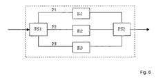
- An inventive multiband filter module for example comprises an inventive frequency splitter FS1 which is adapted to receive signals at different specific frequencies or within frequency bands (related to the frequencies which are addressed by the switch) and transfer said received signals to one of at least two RF-paths and at least one of the RF-paths being connected to a filter.
- Figure 6 shows an inventive multiband filter module with two inventive frequency splitters FS1, FS2 , three RF-paths P1, P2, P3, whereby each of the RF-paths P1, P2, P3 is connected to a filter Fi1, Fi2, Fi3.
- the RF-paths P1, P2, P3 merge in the second frequency splitter FS2, which directs the signal to the single output port of the filter module.
Landscapes
- Transmitters (AREA)
Priority Applications (1)
| Application Number | Priority Date | Filing Date | Title |
|---|---|---|---|
| EP07291104A EP2037530A1 (fr) | 2007-09-13 | 2007-09-13 | Circuit RF commutable et séparateur de fréquences pour applications de bande passante de grande portée |
Applications Claiming Priority (1)
| Application Number | Priority Date | Filing Date | Title |
|---|---|---|---|
| EP07291104A EP2037530A1 (fr) | 2007-09-13 | 2007-09-13 | Circuit RF commutable et séparateur de fréquences pour applications de bande passante de grande portée |
Publications (1)
| Publication Number | Publication Date |
|---|---|
| EP2037530A1 true EP2037530A1 (fr) | 2009-03-18 |
Family
ID=39061696
Family Applications (1)
| Application Number | Title | Priority Date | Filing Date |
|---|---|---|---|
| EP07291104A Ceased EP2037530A1 (fr) | 2007-09-13 | 2007-09-13 | Circuit RF commutable et séparateur de fréquences pour applications de bande passante de grande portée |
Country Status (1)
| Country | Link |
|---|---|
| EP (1) | EP2037530A1 (fr) |
Cited By (3)
| Publication number | Priority date | Publication date | Assignee | Title |
|---|---|---|---|---|
| RU2504869C2 (ru) * | 2012-04-06 | 2014-01-20 | Открытое акционерное общество "Концерн "Созвездие" | Свч переключатель на pin-диодах с фильтрующими свойствами |
| RU2632259C1 (ru) * | 2016-05-24 | 2017-10-03 | Акционерное общество "Научно-производственное предприятие "Исток" имени А.И. Шокина" (АО "НПП "Исток" им. Шокина") | Переключатель СВЧ мощности |
| CN108923791A (zh) * | 2018-06-29 | 2018-11-30 | Oppo广东移动通信有限公司 | 多路选择开关及相关产品 |
Citations (3)
| Publication number | Priority date | Publication date | Assignee | Title |
|---|---|---|---|---|
| EP1237222A1 (fr) * | 2001-02-27 | 2002-09-04 | TELEFONAKTIEBOLAGET LM ERICSSON (publ) | Etage de transformation à bandes multiples pour dispositif à haute fréquence de commutation multi-bande |
| US6496082B1 (en) * | 2001-09-25 | 2002-12-17 | Tyco Electronics Corporation | Matched broadband switch matrix with active diode isolation |
| EP1796203A1 (fr) * | 2005-12-12 | 2007-06-13 | Alcatel Lucent | Commutateur de fréquence pour des applications aux amplificateurs de puissance multibandes et module amplificateur de puissance multibande/multistandard |
-
2007
- 2007-09-13 EP EP07291104A patent/EP2037530A1/fr not_active Ceased
Patent Citations (4)
| Publication number | Priority date | Publication date | Assignee | Title |
|---|---|---|---|---|
| EP1237222A1 (fr) * | 2001-02-27 | 2002-09-04 | TELEFONAKTIEBOLAGET LM ERICSSON (publ) | Etage de transformation à bandes multiples pour dispositif à haute fréquence de commutation multi-bande |
| US6496082B1 (en) * | 2001-09-25 | 2002-12-17 | Tyco Electronics Corporation | Matched broadband switch matrix with active diode isolation |
| EP1796203A1 (fr) * | 2005-12-12 | 2007-06-13 | Alcatel Lucent | Commutateur de fréquence pour des applications aux amplificateurs de puissance multibandes et module amplificateur de puissance multibande/multistandard |
| US20070155345A1 (en) | 2005-12-12 | 2007-07-05 | Alcatel | Frequency switch for multiband power amplifier applications and multiband/multistandard power amplifier module |
Non-Patent Citations (1)
| Title |
|---|
| DE LOS SANTOS H J ET AL: "RF MEMS for ubiquitous wireless connectivity: Part 2 - application", IEEE MICROWAVE MAGAZINE, IEEESERVICE CENTER, PISCATAWAY, NJ, US, vol. 5, no. 4, December 2004 (2004-12-01), pages 50 - 65, XP011124828, ISSN: 1527-3342 * |
Cited By (4)
| Publication number | Priority date | Publication date | Assignee | Title |
|---|---|---|---|---|
| RU2504869C2 (ru) * | 2012-04-06 | 2014-01-20 | Открытое акционерное общество "Концерн "Созвездие" | Свч переключатель на pin-диодах с фильтрующими свойствами |
| RU2632259C1 (ru) * | 2016-05-24 | 2017-10-03 | Акционерное общество "Научно-производственное предприятие "Исток" имени А.И. Шокина" (АО "НПП "Исток" им. Шокина") | Переключатель СВЧ мощности |
| CN108923791A (zh) * | 2018-06-29 | 2018-11-30 | Oppo广东移动通信有限公司 | 多路选择开关及相关产品 |
| CN108923791B (zh) * | 2018-06-29 | 2020-09-25 | Oppo广东移动通信有限公司 | 多路选择开关及相关产品 |
Similar Documents
| Publication | Publication Date | Title |
|---|---|---|
| US8487713B2 (en) | Multiband matching circuit and multiband power amplifier | |
| EP1936814B1 (fr) | Circuit d'adaptation et amplificateur de puissance à double bande | |
| US8416035B2 (en) | Multiband matching circuit | |
| CN109565292B (zh) | 用于多频功率检测的电磁耦合器装置和包含其的设备 | |
| US7656228B2 (en) | Matching circuit and multi-band amplifier | |
| EP2159912A1 (fr) | Amplificateur de Doherty multibande | |
| KR100975607B1 (ko) | 정합 회로 | |
| US8049558B2 (en) | Switchable balanced amplifier | |
| US20070018758A1 (en) | Matching circuit | |
| US20090167458A1 (en) | Matching circuit | |
| US20120235735A1 (en) | Power amplifier circuit and front end circuit | |
| US20190214959A1 (en) | Radio frequency front end circuit and communication apparatus | |
| US7538609B2 (en) | Amplifier, transmitter arrangement having an amplifier and method for amplifying a signal | |
| EP2214311A1 (fr) | Correspondance de circuit multi-bande et d'amplificateur de puissance multi-bande | |
| KR20200039774A (ko) | 멀티플렉서 및 고주파 필터 | |
| KR101912288B1 (ko) | 파워 증폭 시스템의 밴드 선택 스위치 장치 | |
| CN100557955C (zh) | 多频带稳定电路和使用它的多频带放大电路 | |
| US6856187B2 (en) | High frequency switch module | |
| EP2023483B1 (fr) | Banc d'accélérateur destiné à une utilisation dans des modules d'amplificateur de puissance multibande | |
| KR100756221B1 (ko) | 격리 동작 간소화를 위한 시분할 다중 송수신 시스템 | |
| KR20030070198A (ko) | 다중 대역 정합 회로 | |
| KR20090051625A (ko) | 프런트 엔드 모듈 | |
| JP2009239682A (ja) | 周波数可変回路及び周波数可変増幅器 |
Legal Events
| Date | Code | Title | Description |
|---|---|---|---|
| PUAI | Public reference made under article 153(3) epc to a published international application that has entered the european phase |
Free format text: ORIGINAL CODE: 0009012 |
|
| AK | Designated contracting states |
Kind code of ref document: A1 Designated state(s): AT BE BG CH CY CZ DE DK EE ES FI FR GB GR HU IE IS IT LI LT LU LV MC MT NL PL PT RO SE SI SK TR |
|
| AX | Request for extension of the european patent |
Extension state: AL BA HR MK RS |
|
| 17P | Request for examination filed |
Effective date: 20090409 |
|
| AKX | Designation fees paid |
Designated state(s): AT BE BG CH CY CZ DE DK EE ES FI FR GB GR HU IE IS IT LI LT LU LV MC MT NL PL PT RO SE SI SK TR |
|
| 17Q | First examination report despatched |
Effective date: 20100504 |
|
| RAP1 | Party data changed (applicant data changed or rights of an application transferred) |
Owner name: ALCATEL LUCENT |
|
| STAA | Information on the status of an ep patent application or granted ep patent |
Free format text: STATUS: THE APPLICATION HAS BEEN REFUSED |
|
| RAP1 | Party data changed (applicant data changed or rights of an application transferred) |
Owner name: ALCATEL LUCENT |
|
| 18R | Application refused |
Effective date: 20120522 |