EP2037540A2 - Fassung - Google Patents
Fassung Download PDFInfo
- Publication number
- EP2037540A2 EP2037540A2 EP08164084A EP08164084A EP2037540A2 EP 2037540 A2 EP2037540 A2 EP 2037540A2 EP 08164084 A EP08164084 A EP 08164084A EP 08164084 A EP08164084 A EP 08164084A EP 2037540 A2 EP2037540 A2 EP 2037540A2
- Authority
- EP
- European Patent Office
- Prior art keywords
- socket
- contact member
- shell
- base shell
- electrode
- Prior art date
- Legal status (The legal status is an assumption and is not a legal conclusion. Google has not performed a legal analysis and makes no representation as to the accuracy of the status listed.)
- Granted
Links
Images


Classifications
-
- H—ELECTRICITY
- H01—ELECTRIC ELEMENTS
- H01R—ELECTRICALLY-CONDUCTIVE CONNECTIONS; STRUCTURAL ASSOCIATIONS OF A PLURALITY OF MUTUALLY-INSULATED ELECTRICAL CONNECTING ELEMENTS; COUPLING DEVICES; CURRENT COLLECTORS
- H01R33/00—Coupling devices specially adapted for supporting apparatus and having one part acting as a holder providing support and electrical connection via a counterpart which is structurally associated with the apparatus, e.g. lamp holders; Separate parts thereof
- H01R33/02—Single-pole devices, e.g. holder for supporting one end of a tubular incandescent or neon lamp
-
- H—ELECTRICITY
- H01—ELECTRIC ELEMENTS
- H01R—ELECTRICALLY-CONDUCTIVE CONNECTIONS; STRUCTURAL ASSOCIATIONS OF A PLURALITY OF MUTUALLY-INSULATED ELECTRICAL CONNECTING ELEMENTS; COUPLING DEVICES; CURRENT COLLECTORS
- H01R12/00—Structural associations of a plurality of mutually-insulated electrical connecting elements, specially adapted for printed circuits, e.g. printed circuit boards [PCB], flat or ribbon cables, or like generally planar structures, e.g. terminal strips, terminal blocks; Coupling devices specially adapted for printed circuits, flat or ribbon cables, or like generally planar structures; Terminals specially adapted for contact with, or insertion into, printed circuits, flat or ribbon cables, or like generally planar structures
- H01R12/70—Coupling devices
- H01R12/7076—Coupling devices for connection between PCB and component, e.g. display
-
- H—ELECTRICITY
- H01—ELECTRIC ELEMENTS
- H01R—ELECTRICALLY-CONDUCTIVE CONNECTIONS; STRUCTURAL ASSOCIATIONS OF A PLURALITY OF MUTUALLY-INSULATED ELECTRICAL CONNECTING ELEMENTS; COUPLING DEVICES; CURRENT COLLECTORS
- H01R13/00—Details of coupling devices of the kinds covered by groups H01R12/70 or H01R24/00 - H01R33/00
- H01R13/02—Contact members
- H01R13/22—Contacts for co-operating by abutting
- H01R13/24—Contacts for co-operating by abutting resilient; resiliently-mounted
- H01R13/2407—Contacts for co-operating by abutting resilient; resiliently-mounted characterized by the resilient means
- H01R13/2414—Contacts for co-operating by abutting resilient; resiliently-mounted characterized by the resilient means conductive elastomers
-
- H—ELECTRICITY
- H05—ELECTRIC TECHNIQUES NOT OTHERWISE PROVIDED FOR
- H05K—PRINTED CIRCUITS; CASINGS OR CONSTRUCTIONAL DETAILS OF ELECTRIC APPARATUS; MANUFACTURE OF ASSEMBLAGES OF ELECTRICAL COMPONENTS
- H05K3/00—Apparatus or processes for manufacturing printed circuits
- H05K3/30—Assembling printed circuits with electric components, e.g. with resistors
- H05K3/301—Assembling printed circuits with electric components, e.g. with resistors by means of a mounting structure
-
- H—ELECTRICITY
- H01—ELECTRIC ELEMENTS
- H01R—ELECTRICALLY-CONDUCTIVE CONNECTIONS; STRUCTURAL ASSOCIATIONS OF A PLURALITY OF MUTUALLY-INSULATED ELECTRICAL CONNECTING ELEMENTS; COUPLING DEVICES; CURRENT COLLECTORS
- H01R13/00—Details of coupling devices of the kinds covered by groups H01R12/70 or H01R24/00 - H01R33/00
- H01R13/66—Structural association with built-in electrical component
- H01R13/6608—Structural association with built-in electrical component with built-in single component
- H01R13/6641—Structural association with built-in electrical component with built-in single component with diode
-
- H—ELECTRICITY
- H05—ELECTRIC TECHNIQUES NOT OTHERWISE PROVIDED FOR
- H05K—PRINTED CIRCUITS; CASINGS OR CONSTRUCTIONAL DETAILS OF ELECTRIC APPARATUS; MANUFACTURE OF ASSEMBLAGES OF ELECTRICAL COMPONENTS
- H05K2201/00—Indexing scheme relating to printed circuits covered by H05K1/00
- H05K2201/10—Details of components or other objects attached to or integrated in a printed circuit board
- H05K2201/10007—Types of components
- H05K2201/10106—Light emitting diode [LED]
-
- H—ELECTRICITY
- H05—ELECTRIC TECHNIQUES NOT OTHERWISE PROVIDED FOR
- H05K—PRINTED CIRCUITS; CASINGS OR CONSTRUCTIONAL DETAILS OF ELECTRIC APPARATUS; MANUFACTURE OF ASSEMBLAGES OF ELECTRICAL COMPONENTS
- H05K2201/00—Indexing scheme relating to printed circuits covered by H05K1/00
- H05K2201/10—Details of components or other objects attached to or integrated in a printed circuit board
- H05K2201/10227—Other objects, e.g. metallic pieces
- H05K2201/10325—Sockets, i.e. female type connectors comprising metallic connector elements integrated in, or bonded to a common dielectric support
Definitions
- This invention relates to a socket for an element such as an LED (Light Emitting Diode) element.
- LED elements are generally robust and have high luminous efficiencies. However, they generate a large amount of heat that causes a problem. Therefore, heat dissipation should be considered.
- Heat dissipation technologies are disclosed in, for example, JP-A 2001-15186 and JP-A 2006-331801 .
- a socket is provided with a heat sink.
- the heat sink hinders miniaturization of the socket.
- a socket is provided with a heat dissipation member.
- a technique for connecting an LED element to the socket is not limited.
- a socket for an element with an element electrode comprising a base shell, a cover shell engaged with the base shell so that the base shell and the cover shell define a cavity, and a contact member comprising an elastic member and a contact electrode provided on the elastic member.
- the contact member is designed and arranged so that the element is mountable on the contact member within the cavity with the element electrode connected to the contact electrode.
- Fig. 1 is an exploded perspective view of a socket according to an embodiment of the present invention
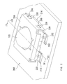
- Fig. 2 is a perspective view of the socket of Fig. 1 ;
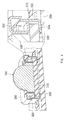
- Fig. 3 is a cross sectional view of the socket, taken along lines III-III of Fig. 2 ;
- Fig. 4 is a cross sectional view of the socket, taken along lines IV-IV of Fig. 3 .
- a socket 300 is used for connecting an LED (Light Emitting Diode) element 100 and a substrate 200.
- the LED element 100 comprises an anode 110 and a cathode 120.
- the substrate 200 is provided with two pads 210 and 214 and four ground pads 212.
- the socket 300 comprises a contact member 310, a base shell 330 and a cover shell 350.
- the cover shell 350 is engaged with the base shell 330 so that the base shell 330 and the cover shell 350 define a cavity that can accommodate the contact member 310 and the LED element 100 at least in part.
- the base shell 330 has a frame which is made of a high thermal-conductive material.
- the base shell 330 is provided with four hold down portions 332, heat-transfer fins 334, four position-fins 336 and four engage-tongues 338.
- Each hold down portion 332 extends outward from a bottom edge of the frame.
- the base shell 330 is fixed to the substrate 200 by soldering the hold down portions 332 to the ground pads 212.
- Each heat-transfer fin 334 extends inward from the bottom edge of the frame.
- Each position-fin 336 extends inward from a top edge of the frame.
- Each position-fin 336 has an inverted L-shape which has an end extending downwards.
- Each engage-tongue 338 projects outward from the frame by making an U-shaped cut on the frame followed by bending the cut portion outward.
- the contact member 310 of this embodiment comprises two plate-like elastic blocks 312, an insulation film 314 and two electrodes 316 and 318.
- Each elastic block 312 has an upper top surface and a lower surface.
- the insulation film 314 is attached to the elastic blocks 312.
- the electrodes 316 and 318 are made of conductive films which are formed on the insulation film 314 and correspond to the elastic blocks 312, respectively.
- the electrode 316 covers the upper surface and the lower surface of one of the elastic blocks 312 with the insulation film 314 interposed between the electrode 316 and the elastic block 312.
- the electrode 318 covers the upper surface and the lower surface of the other elastic blocks 312 with insulation film 314 interposed between the electrode 318 and the other elastic block 312.
- the contact member 310 is arranged in the frame of the base shell 330; the electrode 316 is electrically connected to the pad 214; the electrode 318 is electrically connected to the pad 210 and is brought into contact with the heat-transfer fin 334. As understood from Figs. 1 and 2 , the contact member 310 of the present embodiment allows various different arrangements of the pads 210 and 214 because the electrodes 318 and 316 have large areas.
- the cover shell 350 of this embodiment is made of a high thermal-conductive material similarly to the base shell 330.
- the cover shell 350 has two binding-fins 352, an opening 354 and four windows 356.
- the binding-fins 352 are formed to correspond to the heat-transfer fins 334, respectively.
- the opening 354 allows a part of the LED element 100 to project from the cover shell 350 when the LED element 100 is partially accommodated in the cavity.
- the four windows 356 correspond to the engage-tongues 338, respectively and are engaged with the four windows 356 so that the base shell 330 and the cover shell 350 are combined and define the aforementioned cavity.
- the LED element 100 is mounted on the contact member 310 so that the anode 110 and the cathode 120 are electrically connected to the pads 214 and 210 through the electrodes 316 and 318, respectively.
- the cover shell 350 is engaged with the base shell 330.
- the contact member 310 and the LED element 100 are accommodated within the cavity, while a part of the LED element 100 project from the cover shell 350, as shown in Fig. 2 .
- the contact member 310 is held between the binding-fins 352 and the heat-transfer fins 334.
- the binding fins 352 serve to adjust position of the LED element 100 in the cavity.
- the LED element 100 is thermally coupled to the contact member 310.
- the contact member is thermally coupled to the base shell 330 and the cover shell 350 through the heat-transfer fins 334 and the binding-fins 352, respectively. Therefore, even if the LED element 100 generates heat, the heat is transferred through the contact member 310 to the base shell 330 and the cover shell 350 so that they dissipate the heat.
- each of the base shell 330 and the cover shell 350 serves to a heat sink.
- the contact member 310 has a large area on which the LED element 100 is mounted. The large area of the contact member 310 can also dissipate the heat of the LED element 100.
- the socket 300 of this embodiment has a high improved heat-dissipation property.
- the contact member 310 of the embodiment comprises the elastic blocks 312, the contact member 310 may comprise packed gel-like elastic members instead thereof.
- Each of the elastic blocks 312 may be made of a material having a heat-dissipation property, such as a silicone rubber. The heat-dissipation material of the elastic blocks 312 further improve the heat-dissipation property of the socket 300.
Landscapes
- Engineering & Computer Science (AREA)
- Manufacturing & Machinery (AREA)
- Microelectronics & Electronic Packaging (AREA)
- Led Device Packages (AREA)
- Connecting Device With Holders (AREA)
- Led Devices (AREA)
Applications Claiming Priority (1)
| Application Number | Priority Date | Filing Date | Title |
|---|---|---|---|
| JP2007239803A JP4391555B2 (ja) | 2007-09-14 | 2007-09-14 | ソケット |
Publications (3)
| Publication Number | Publication Date |
|---|---|
| EP2037540A2 true EP2037540A2 (de) | 2009-03-18 |
| EP2037540A3 EP2037540A3 (de) | 2010-03-10 |
| EP2037540B1 EP2037540B1 (de) | 2012-11-21 |
Family
ID=39885113
Family Applications (1)
| Application Number | Title | Priority Date | Filing Date |
|---|---|---|---|
| EP08164084A Not-in-force EP2037540B1 (de) | 2007-09-14 | 2008-09-10 | Fassung |
Country Status (6)
| Country | Link |
|---|---|
| US (1) | US7771211B2 (de) |
| EP (1) | EP2037540B1 (de) |
| JP (1) | JP4391555B2 (de) |
| KR (1) | KR101007852B1 (de) |
| CN (1) | CN101388514B (de) |
| TW (1) | TWI374586B (de) |
Cited By (4)
| Publication number | Priority date | Publication date | Assignee | Title |
|---|---|---|---|---|
| GB2474268A (en) * | 2009-10-09 | 2011-04-13 | Su-Hsin Yeh | Replaceable LED Light Structure |
| WO2011086192A1 (de) * | 2010-01-18 | 2011-07-21 | Axelmeiselicht Gmbh | Vorrichtung zur fassung von led-leuchtmitteln |
| EP2040518A3 (de) * | 2007-09-18 | 2012-03-28 | Japan Aviation Electronics Industry, Limited | Wärmeübertragungselement und -verbinder |
| EP2362449B1 (de) * | 2010-02-18 | 2016-12-28 | LG Innotek Co., Ltd. | Elektrodenanordnung für eine lichtemittierende Vorrichtung und entsprechendes Gehäuse |
Families Citing this family (13)
| Publication number | Priority date | Publication date | Assignee | Title |
|---|---|---|---|---|
| JP5320181B2 (ja) * | 2009-06-19 | 2013-10-23 | 日本航空電子工業株式会社 | 電気接続部材およびそれを用いたソケットコネクタ |
| KR101047438B1 (ko) * | 2009-10-23 | 2011-07-08 | 주식회사 일흥 | 엘이디소켓 일체형 램프 구동장치 |
| KR101047437B1 (ko) * | 2009-10-23 | 2011-07-08 | 주식회사 일흥 | 엘이디소켓 일체형 램프 장치 |
| JP5517239B2 (ja) * | 2009-11-10 | 2014-06-11 | 日本航空電子工業株式会社 | コネクタ |
| US8210715B2 (en) * | 2009-12-09 | 2012-07-03 | Tyco Electronics Corporation | Socket assembly with a thermal management structure |
| US8226280B2 (en) * | 2010-04-28 | 2012-07-24 | Tyco Electronics Corporation | LED socket assembly |
| JP5340248B2 (ja) * | 2010-10-28 | 2013-11-13 | 京セラコネクタプロダクツ株式会社 | 発光半導体素子接続用コネクタ |
| JP5845029B2 (ja) * | 2011-09-16 | 2016-01-20 | 日本航空電子工業株式会社 | ハウジングレスコネクタ |
| JP5499005B2 (ja) | 2011-10-25 | 2014-05-21 | 京セラコネクタプロダクツ株式会社 | 半導体発光素子用ホルダ、半導体発光素子モジュール、及び、照明器具 |
| TWM461207U (zh) * | 2013-03-19 | 2013-09-01 | Tuton Technology Co Ltd | 可感測接近物的電源插座 |
| CN108847441B (zh) * | 2018-06-26 | 2019-10-29 | 浙江飞天光电股份有限公司 | 一种高效散热的发光二极管 |
| EP4475639A1 (de) * | 2023-06-05 | 2024-12-11 | Magna Electronics Sweden AB | Halter für eine oberflächenmontierbare vorrichtung, anordnung und schaltungsträger |
| JP2025178704A (ja) * | 2024-05-27 | 2025-12-09 | 株式会社日本マイクロニクス | 電気的接続装置、gnd端子接触部材及びハウジング部材 |
Citations (3)
| Publication number | Priority date | Publication date | Assignee | Title |
|---|---|---|---|---|
| JP2001015186A (ja) | 1999-06-30 | 2001-01-19 | Showa Alum Corp | 集積回路の接地構造 |
| EP1355384A2 (de) | 2002-04-09 | 2003-10-22 | Japan Aviation Electronics Industry, Limited | Kartensteckverbinder mit reduziertem Kraftaufwand bei der Benutzung |
| JP2006331801A (ja) | 2005-05-25 | 2006-12-07 | Matsushita Electric Works Ltd | 電子部品用ソケット |
Family Cites Families (12)
| Publication number | Priority date | Publication date | Assignee | Title |
|---|---|---|---|---|
| US3998512A (en) * | 1975-02-13 | 1976-12-21 | International Telephone And Telegraph Corporation | Electrical connector |
| US4761140A (en) | 1987-02-20 | 1988-08-02 | Augat Inc. | Minimum insertion force self-cleaning anti-overstress PLCC receiving socket |
| US5273440A (en) * | 1992-05-19 | 1993-12-28 | Elco Corporation | Pad array socket |
| JP3281180B2 (ja) | 1994-06-02 | 2002-05-13 | 株式会社アドバンテスト | Icソケット構造 |
| JP2876292B2 (ja) | 1995-01-20 | 1999-03-31 | 信越ポリマー株式会社 | コネクタおよびコネクタの製造方法 |
| JP2004006199A (ja) | 2001-12-27 | 2004-01-08 | Moldec Kk | 集積回路用コネクタと、集積回路装着用組立体 |
| US20030236007A1 (en) * | 2002-06-25 | 2003-12-25 | Lye Poh Huat | Connector for an electronic component |
| JP3842223B2 (ja) | 2003-01-23 | 2006-11-08 | 日本航空電子工業株式会社 | コネクタ |
| TW200536204A (en) * | 2004-04-16 | 2005-11-01 | Top Yang Technology Entpr Co | Electric connector |
| US7814024B2 (en) * | 2004-05-14 | 2010-10-12 | Ching Peter N | Multi-way transactions related data exchange apparatus and methods |
| JP4179620B2 (ja) * | 2005-04-28 | 2008-11-12 | 日本航空電子工業株式会社 | コネクタ |
| FR2885263B1 (fr) | 2005-04-29 | 2007-07-13 | Johnson Controls Tech Co | Dispositif electronique comportant un connecteur elastomere feuillete, et procede d'assemblage |
-
2007
- 2007-09-14 JP JP2007239803A patent/JP4391555B2/ja not_active Expired - Fee Related
-
2008
- 2008-09-03 TW TW097133706A patent/TWI374586B/zh not_active IP Right Cessation
- 2008-09-04 US US12/231,645 patent/US7771211B2/en not_active Expired - Fee Related
- 2008-09-05 KR KR1020080087619A patent/KR101007852B1/ko not_active Expired - Fee Related
- 2008-09-10 EP EP08164084A patent/EP2037540B1/de not_active Not-in-force
- 2008-09-12 CN CN2008101491344A patent/CN101388514B/zh not_active Expired - Fee Related
Patent Citations (3)
| Publication number | Priority date | Publication date | Assignee | Title |
|---|---|---|---|---|
| JP2001015186A (ja) | 1999-06-30 | 2001-01-19 | Showa Alum Corp | 集積回路の接地構造 |
| EP1355384A2 (de) | 2002-04-09 | 2003-10-22 | Japan Aviation Electronics Industry, Limited | Kartensteckverbinder mit reduziertem Kraftaufwand bei der Benutzung |
| JP2006331801A (ja) | 2005-05-25 | 2006-12-07 | Matsushita Electric Works Ltd | 電子部品用ソケット |
Cited By (5)
| Publication number | Priority date | Publication date | Assignee | Title |
|---|---|---|---|---|
| EP2040518A3 (de) * | 2007-09-18 | 2012-03-28 | Japan Aviation Electronics Industry, Limited | Wärmeübertragungselement und -verbinder |
| GB2474268A (en) * | 2009-10-09 | 2011-04-13 | Su-Hsin Yeh | Replaceable LED Light Structure |
| GB2474268B (en) * | 2009-10-09 | 2012-01-18 | Su-Hsin Yeh | LED light structure |
| WO2011086192A1 (de) * | 2010-01-18 | 2011-07-21 | Axelmeiselicht Gmbh | Vorrichtung zur fassung von led-leuchtmitteln |
| EP2362449B1 (de) * | 2010-02-18 | 2016-12-28 | LG Innotek Co., Ltd. | Elektrodenanordnung für eine lichtemittierende Vorrichtung und entsprechendes Gehäuse |
Also Published As
| Publication number | Publication date |
|---|---|
| TWI374586B (en) | 2012-10-11 |
| KR20090028415A (ko) | 2009-03-18 |
| KR101007852B1 (ko) | 2011-01-14 |
| CN101388514B (zh) | 2012-02-29 |
| US7771211B2 (en) | 2010-08-10 |
| CN101388514A (zh) | 2009-03-18 |
| EP2037540B1 (de) | 2012-11-21 |
| EP2037540A3 (de) | 2010-03-10 |
| JP4391555B2 (ja) | 2009-12-24 |
| TW200915671A (en) | 2009-04-01 |
| US20090075510A1 (en) | 2009-03-19 |
| JP2009070738A (ja) | 2009-04-02 |
Similar Documents
| Publication | Publication Date | Title |
|---|---|---|
| EP2037540A2 (de) | Fassung | |
| EP2083214B1 (de) | Leuchtdiodenlampe | |
| US6966674B2 (en) | Backlight module and heat dissipation structure thereof | |
| TWI495143B (zh) | 功率式表面安裝之發光晶粒封裝 | |
| JP3736366B2 (ja) | 表面実装型発光素子およびそれを用いた発光装置 | |
| CN102187149B (zh) | 用于在两个可连接构件之间导热的系统 | |
| JP6768612B2 (ja) | 半導体装置 | |
| US4004195A (en) | Heat-sink assembly for high-power stud-mounted semiconductor device | |
| US20070098334A1 (en) | Light emitting device | |
| JP2002299700A (ja) | Led照明装置 | |
| WO2009110045A1 (ja) | 発熱体搭載部品の取付構造 | |
| GB0009879D0 (en) | Light emitting diode device | |
| US20080246383A1 (en) | LED-lamp heat-dissipation device | |
| US20090010011A1 (en) | Solid state lighting device with heat-dissipating capability | |
| JP5102455B2 (ja) | Led発光装置 | |
| JP2013211579A (ja) | 発光ダイオード装置 | |
| US7598535B2 (en) | Light-emitting diode assembly and method of fabrication | |
| JP2009021384A (ja) | 電子部品及び発光装置 | |
| JP7021444B2 (ja) | 発光モジュール | |
| KR102148846B1 (ko) | 인쇄회로기판 조립체 및 이를 포함하는 발광장치 | |
| JP3128613U (ja) | 発光ダイオード | |
| JP2006269782A (ja) | 発光ダイオード | |
| JP2009021383A (ja) | 電子部品 | |
| KR101801195B1 (ko) | 조명모듈 제조방법 및 이에 의하여 제조되는 조명모듈 | |
| JP3128614U (ja) | 発光ダイオード |
Legal Events
| Date | Code | Title | Description |
|---|---|---|---|
| PUAI | Public reference made under article 153(3) epc to a published international application that has entered the european phase |
Free format text: ORIGINAL CODE: 0009012 |
|
| AK | Designated contracting states |
Kind code of ref document: A2 Designated state(s): AT BE BG CH CY CZ DE DK EE ES FI FR GB GR HR HU IE IS IT LI LT LU LV MC MT NL NO PL PT RO SE SI SK TR |
|
| AX | Request for extension of the european patent |
Extension state: AL BA MK RS |
|
| PUAL | Search report despatched |
Free format text: ORIGINAL CODE: 0009013 |
|
| AK | Designated contracting states |
Kind code of ref document: A3 Designated state(s): AT BE BG CH CY CZ DE DK EE ES FI FR GB GR HR HU IE IS IT LI LT LU LV MC MT NL NO PL PT RO SE SI SK TR |
|
| AX | Request for extension of the european patent |
Extension state: AL BA MK RS |
|
| RIC1 | Information provided on ipc code assigned before grant |
Ipc: H01R 12/16 20060101ALI20100204BHEP Ipc: H01R 13/24 20060101AFI20100204BHEP |
|
| 17P | Request for examination filed |
Effective date: 20100910 |
|
| AKX | Designation fees paid |
Designated state(s): DE FR |
|
| 17Q | First examination report despatched |
Effective date: 20110118 |
|
| REG | Reference to a national code |
Ref country code: DE Ref legal event code: R079 Ref document number: 602008020213 Country of ref document: DE Free format text: PREVIOUS MAIN CLASS: H01R0013220000 Ipc: H01R0012700000 |
|
| GRAP | Despatch of communication of intention to grant a patent |
Free format text: ORIGINAL CODE: EPIDOSNIGR1 |
|
| RIC1 | Information provided on ipc code assigned before grant |
Ipc: H01R 13/24 20060101ALI20120611BHEP Ipc: H01R 12/70 20110101AFI20120611BHEP |
|
| GRAS | Grant fee paid |
Free format text: ORIGINAL CODE: EPIDOSNIGR3 |
|
| GRAA | (expected) grant |
Free format text: ORIGINAL CODE: 0009210 |
|
| AK | Designated contracting states |
Kind code of ref document: B1 Designated state(s): DE FR |
|
| REG | Reference to a national code |
Ref country code: DE Ref legal event code: R096 Ref document number: 602008020213 Country of ref document: DE Effective date: 20130117 |
|
| PLBE | No opposition filed within time limit |
Free format text: ORIGINAL CODE: 0009261 |
|
| STAA | Information on the status of an ep patent application or granted ep patent |
Free format text: STATUS: NO OPPOSITION FILED WITHIN TIME LIMIT |
|
| 26N | No opposition filed |
Effective date: 20130822 |
|
| PGFP | Annual fee paid to national office [announced via postgrant information from national office to epo] |
Ref country code: DE Payment date: 20130930 Year of fee payment: 6 |
|
| REG | Reference to a national code |
Ref country code: DE Ref legal event code: R097 Ref document number: 602008020213 Country of ref document: DE Effective date: 20130822 |
|
| PGFP | Annual fee paid to national office [announced via postgrant information from national office to epo] |
Ref country code: FR Payment date: 20130918 Year of fee payment: 6 |
|
| REG | Reference to a national code |
Ref country code: DE Ref legal event code: R119 Ref document number: 602008020213 Country of ref document: DE |
|
| REG | Reference to a national code |
Ref country code: FR Ref legal event code: ST Effective date: 20150529 |
|
| PG25 | Lapsed in a contracting state [announced via postgrant information from national office to epo] |
Ref country code: DE Free format text: LAPSE BECAUSE OF NON-PAYMENT OF DUE FEES Effective date: 20150401 |
|
| PG25 | Lapsed in a contracting state [announced via postgrant information from national office to epo] |
Ref country code: FR Free format text: LAPSE BECAUSE OF NON-PAYMENT OF DUE FEES Effective date: 20140930 |