EP2040328A1 - Dispositif d'antenne - Google Patents
Dispositif d'antenne Download PDFInfo
- Publication number
- EP2040328A1 EP2040328A1 EP07767927A EP07767927A EP2040328A1 EP 2040328 A1 EP2040328 A1 EP 2040328A1 EP 07767927 A EP07767927 A EP 07767927A EP 07767927 A EP07767927 A EP 07767927A EP 2040328 A1 EP2040328 A1 EP 2040328A1
- Authority
- EP
- European Patent Office
- Prior art keywords
- ground
- substrate
- antenna
- ground conductor
- conductor
- Prior art date
- Legal status (The legal status is an assumption and is not a legal conclusion. Google has not performed a legal analysis and makes no representation as to the accuracy of the status listed.)
- Granted
Links
Images


Classifications
-
- H—ELECTRICITY
- H01—ELECTRIC ELEMENTS
- H01Q—ANTENNAS, i.e. RADIO AERIALS
- H01Q1/00—Details of, or arrangements associated with, antennas
- H01Q1/12—Supports; Mounting means
- H01Q1/22—Supports; Mounting means by structural association with other equipment or articles
- H01Q1/24—Supports; Mounting means by structural association with other equipment or articles with receiving set
- H01Q1/241—Supports; Mounting means by structural association with other equipment or articles with receiving set used in mobile communications, e.g. GSM
- H01Q1/242—Supports; Mounting means by structural association with other equipment or articles with receiving set used in mobile communications, e.g. GSM specially adapted for hand-held use
- H01Q1/243—Supports; Mounting means by structural association with other equipment or articles with receiving set used in mobile communications, e.g. GSM specially adapted for hand-held use with built-in antennas
-
- H—ELECTRICITY
- H01—ELECTRIC ELEMENTS
- H01Q—ANTENNAS, i.e. RADIO AERIALS
- H01Q1/00—Details of, or arrangements associated with, antennas
- H01Q1/12—Supports; Mounting means
- H01Q1/22—Supports; Mounting means by structural association with other equipment or articles
- H01Q1/24—Supports; Mounting means by structural association with other equipment or articles with receiving set
-
- H—ELECTRICITY
- H01—ELECTRIC ELEMENTS
- H01Q—ANTENNAS, i.e. RADIO AERIALS
- H01Q1/00—Details of, or arrangements associated with, antennas
- H01Q1/36—Structural form of radiating elements, e.g. cone, spiral, umbrella; Particular materials used therewith
- H01Q1/362—Structural form of radiating elements, e.g. cone, spiral, umbrella; Particular materials used therewith for broadside radiating helical antennas
-
- H—ELECTRICITY
- H01—ELECTRIC ELEMENTS
- H01Q—ANTENNAS, i.e. RADIO AERIALS
- H01Q1/00—Details of, or arrangements associated with, antennas
- H01Q1/36—Structural form of radiating elements, e.g. cone, spiral, umbrella; Particular materials used therewith
- H01Q1/38—Structural form of radiating elements, e.g. cone, spiral, umbrella; Particular materials used therewith formed by a conductive layer on an insulating support
-
- H—ELECTRICITY
- H01—ELECTRIC ELEMENTS
- H01Q—ANTENNAS, i.e. RADIO AERIALS
- H01Q1/00—Details of, or arrangements associated with, antennas
- H01Q1/48—Earthing means; Earth screens; Counterpoises
-
- H—ELECTRICITY
- H01—ELECTRIC ELEMENTS
- H01Q—ANTENNAS, i.e. RADIO AERIALS
- H01Q9/00—Electrically-short antennas having dimensions not more than twice the operating wavelength and consisting of conductive active radiating elements
- H01Q9/04—Resonant antennas
- H01Q9/30—Resonant antennas with feed to end of elongated active element, e.g. unipole
- H01Q9/40—Element having extended radiating surface
Definitions
- the present invention relates to an antenna apparatus suitable for downsizing radio communication equipment.
- an antenna apparatus as disclosed in, for example, Japanese Patent No. 3758495 is proposed.
- a spiral conductor layer is formed on the surface of a base material made of a dielectric material or a magnetic material.
- a so-called chip antenna is installed on a substrate, and the chip antenna is grounded to a ground plane formed on the substrate.
- an RF ground conductor 3 to which a chip antenna 2 on a substrate 1 is grounded ideally requires the most area on the substrate 1 in order to gain sufficient antenna characteristics.
- a circuit ground conductor 4 to be used as a digital circuit ground has been formed on a substrate 1 together with an RF ground conductor 3 to which a chip antenna 2 is grounded, to thereby allow the coexistence of the RF ground conductor 3 and the circuit ground conductor 4 on the same substrate 1, as shown in FIG. 6 .
- the present invention has been achieved in view of the aforementioned problems, and has an object to provide an antenna apparatus that is capable of obtaining the antenna characteristics similar to those in a case where an RF ground conductor is formed wide on a substrate, and also allows coexistence of the RF ground conductor and a circuit ground conductor on the same substrate.
- the present invention adopts the following in order to solve the above problems.
- An antenna apparatus of the present invention includes: an RF ground conductor which is branched to extend in at least two directions, at least a part of which is formed on a surface of the substrate, the RF ground conductor functioning as an antenna ground plane; and an antenna portion, one end of which is connected to the RF ground conductor.
- the RF ground conductor is branched to extend in at least two directions. Therefore, in spite of the small ground area as a whole, the RF ground conductor extends in two directions to secure a length necessary for antenna characteristics. As a result, a radiation efficiency similar to that of a ground with one large area is obtained, making it possible to have sufficient antenna characteristics.
- the RF ground conductor be formed in an inverted L-shape branched in two directions orthogonal to each other.
- This antenna apparatus has the RF ground conductor branched in an inverted L-shape. Therefore, when a rectangular substrate is used, the RF ground conductor is arranged along a short edge and a long edge of the substrate. As a result, it is possible to effectively use the surface of the substrate. Furthermore, the RF ground conductor is branched in directions orthogonal to each other. This can contribute to antenna characteristics in an omnidirectional manner.
- the antenna portion be a chip antenna installed on the substrate, and that the RF ground conductor have, on the substrate: a first ground portion that extends along the chip antenna; and a second ground portion that extends in a direction orthogonal to an extension direction of the first ground portion and also in a direction of spacing apart from the first ground portion and the chip antenna.
- the RF ground conductor is made of: the first ground portion along the chip antenna; and the second ground portion perpendicular to the chip antenna. Therefore, the arrangement of the chip antenna in the arrangement relationship as described above makes it possible to obtain favorable antenna characteristics even in a small space.
- the RF ground conductor include: a substrate ground portion formed on the substrate; and an external ground portion, a base end of which is connected to the substrate ground portion and extends outside the substrate in a direction different from that of the substrate ground portion.
- the RF ground conductor is made of: the substrate ground portion; and the external ground portion. Therefore, in the case where a sufficient ground plane is not available on the surface of the substrate, it is possible to secure a ground length by use of the external ground portion such as a metal wire outside the substrate, to thereby obtain favorable antenna characteristics.
- a circuit ground conductor functioning as a digital circuit ground be formed on the surface of the substrate.
- the circuit ground conductor is formed on the substrate together with the RF ground conductor. This makes it possible to secure a sufficient area for the circuit ground conductor while maintaining the antenna characteristics.
- the RF ground conductor is branched to extend in at least two directions.
- a radiation efficiency similar to that of a ground with one large area is obtained, making it possible to have sufficient antenna characteristics. Therefore, even if a circuit ground conductor functioning as a digital circuit ground is brought into coexistence with an RF ground conductor on the same substrate, sufficient antenna characteristics are obtained. As a result, it is possible to achieve a high packaging density of parts and a downsizing of radio communication equipment.
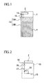
- An antenna apparatus 1 of the present embodiment includes: a rectangular substrate 1; an RF ground conductor 13; a chip antenna (antenna portion) 2; and a circuit ground conductor 4.
- the substrate 1 is made of an insulative material such as a resin.
- the RF ground conductor 13 is formed on a surface of the substrate 1, and functions as an antenna ground plane.
- the chip antenna 2 has its one end connected to the RF ground conductor 13.
- the circuit ground conductor 4 is formed on the surface of the substrate 1, and functions as a digital circuit ground.
- the above chip antenna 2 is an antenna element that functions as a loading element. It includes: a rectangular base material made of a dielectric such as, for example, an alumina; a linear conductor pattern that is wound in a spiral manner with respect to the longitudinal direction of a surface of this base material.
- This chip antenna 2 is installed at a position close to one of the short edges of the substrate 1 and spaced a predetermined distance apart from the RF ground conductor 13. It is fixed onto a land (not shown in the figure) formed at a predetermined position on the substrate 1. Furthermore, the chip antenna 2 is connected to the RF ground conductor 13 via a link conductor 14. Note that the conductor pattern of the chip antenna 2 has its one end connected to the link conductor 14.
- This frequency regulation circuit 15 includes: a first inductor 16 and a second inductor 17 that are chip inductors connected in series to the chip antenna 2; and a third inductor 18 that is a chip inductor whose one end is connected to the second inductor 17 and whose other end is connected to the RF ground conductor 13. Furthermore, between the second inductor 17 and the third inductor 18, there is provided a feeding point. Note that the first inductor 16 and the second inductor 17 are for regulating resonant frequencies, and that the third inductor 18 is provided for reducing reflections of incident powers.
- the above RF ground conductor 13 is for example pattern-formed on the substrate 1 with a copper foil or the like, and is also connected to a ground of a high-frequency circuit (not shown in the figure).
- the RF ground conductor 13 has a first ground portion 19A and a second ground portion 19B.
- the first ground portion 19A extends along the chip antenna 2.
- the second ground portion 19B extends in a direction orthogonal to an extension direction of the first ground portion 19A and also in a direction of spacing apart from the first ground portion 19A and the chip antenna 2. That is, the RF ground conductor 13 is formed in an inverted L-shape branched to extend in two directions orthogonal to each other.
- the second ground portion 19B is arranged on the link conductor 14 side (in the figure, on the left side of the circuit ground conductor 4) along the circuit ground conductor 4.
- the RF ground conductor 13 is branched to extend in two directions as the first ground portion 19A and the second ground portion 19B. Therefore, in spite of the small ground area as a whole, the RF ground conductor 13 extends in two directions to secure a length necessary for the antenna characteristics. As a result, a radiation efficiency similar to that of a ground with one large area is obtained, making it possible to have sufficient antenna characteristics. Note that in the RF ground conductor 13 branched in two directions, a combination with the chip antenna 2 as an antenna portion brings about a bipolar-antenna-like state. Therefore, it is assumed that a length close to 1/4 of an antenna operating wavelength is formed as an electrical length, thus improving the antenna characteristics.
- the antenna apparatus of the present embodiment has the RF ground conductor 13 branched in an inverted L-shape. Therefore, it is possible to effectively use the surface of the substrate 1 by arranging the first ground portion 19A and the second ground portion 19B respectively along a short edge and a long edge of the substrate 1.
- the circuit ground conductor 4 is formed on the substrate 1 together with the RF ground conductor 13. This makes it possible to secure a sufficient area of the circuit ground conductor 4 while maintaining the antenna characteristics.
- the RF ground conductor 13 is branched in directions orthogonal to each other. This can contribute to the antenna characteristics in an omnidirectional manner.
- the second ground portion 19B may be arranged on the opposite side of the link conductor 14 (in the figure, on the right side of the circuit ground conductor 4) along the circuit ground conductor 4, as shown in FIG. 3 .
- the antenna apparatus of the second embodiment is made of: a substrate ground portion 29A where an RF ground conductor 23 is formed on a substrate 1; and an external ground portion 29B a base end of which is connected to the substrate ground portion 29A and extends outside the substrate 1 in a direction different from that of the substrate ground portion 29A, as shown in FIG. 4 .
- the RF ground conductor 23 is made of: the substrate ground portion 29A that is pattern-formed on the substrate 1, similarly to the first ground portion 19A; and the external ground portion 29B whose base end is connected to the left edge of the substrate ground portion 29A and which extends along the circuit ground conductor 4 in a direction orthogonal to an extension direction of the substrate ground portion 29A.
- the RF ground conductor 23 is made of: the substrate ground portion 29A; and the external ground portion 29B. Therefore, in the case where a sufficient ground plane is not available on the surface of the substrate 1 for securing the circuit ground conductor 4 or for other purposes, it is possible to secure a ground length by use of the external ground portion 29B outside the substrate 1, to thereby obtain favorable antenna characteristics.
- the regulator circuit constants of the first inductor 16 to the third inductor 18 in the frequency regulation circuit 15 were respectively made A, B, and C. Furthermore, as constituent materials of the respective parts, an FR-4 with a specific inductive capacity of 4.9 was used in the substrate 1, and also an alumina base material with a specific inductive capacity of 9 was used in the chip antenna 2. The conductors in the conductor pattern and the surface of the substrate 1 were perfect conductors.
- Table 1 shows the results of the evaluation confirming the effect by the simulation tool performed on the above-mentioned first embodiment (Invention 1) and another example of the first embodiment (Invention 2) based on the above calculation conditions. Table 1 also shows the results of the simulation similarly performed on an ideal configuration (Ideal Example) shown in FIG. 5 and a conventional configuration (Conventional Example) shown in FIG. 6 .
- the first inductor 16 to the third inductor 18 with an inductance component as a lumped constant element are used.
- the component is not limited to an inductance component. Capacitors with a capacitance component may be used. Alternatively, these may be combined.
- an alumina which is a dielectric material.
- a magnetic material or a composite material combining a dielectric material and a magnetic material may be used.
- the above RF ground conductors 13 and 23 are branched to extend in two directions.
- the RF ground conductor may be branched to extend in three or more directions.
Landscapes
- Engineering & Computer Science (AREA)
- Computer Networks & Wireless Communication (AREA)
- Details Of Aerials (AREA)
- Support Of Aerials (AREA)
Applications Claiming Priority (2)
| Application Number | Priority Date | Filing Date | Title |
|---|---|---|---|
| JP2006180513A JP4688068B2 (ja) | 2006-06-29 | 2006-06-29 | アンテナ装置 |
| PCT/JP2007/063142 WO2008001899A1 (fr) | 2006-06-29 | 2007-06-29 | Dispositif d'antenne |
Publications (3)
| Publication Number | Publication Date |
|---|---|
| EP2040328A1 true EP2040328A1 (fr) | 2009-03-25 |
| EP2040328A4 EP2040328A4 (fr) | 2010-04-21 |
| EP2040328B1 EP2040328B1 (fr) | 2013-05-22 |
Family
ID=38845662
Family Applications (1)
| Application Number | Title | Priority Date | Filing Date |
|---|---|---|---|
| EP07767927.2A Not-in-force EP2040328B1 (fr) | 2006-06-29 | 2007-06-29 | Dispositif d'antenne |
Country Status (8)
| Country | Link |
|---|---|
| US (1) | US7982682B2 (fr) |
| EP (1) | EP2040328B1 (fr) |
| JP (1) | JP4688068B2 (fr) |
| KR (1) | KR101367586B1 (fr) |
| CN (1) | CN101479879B (fr) |
| ES (1) | ES2425369T3 (fr) |
| TW (1) | TWI440251B (fr) |
| WO (1) | WO2008001899A1 (fr) |
Cited By (1)
| Publication number | Priority date | Publication date | Assignee | Title |
|---|---|---|---|---|
| EP2168205A4 (fr) * | 2007-07-18 | 2012-06-06 | Nokia Corp | Arrangement d'antenne |
Families Citing this family (9)
| Publication number | Priority date | Publication date | Assignee | Title |
|---|---|---|---|---|
| FI20085304A0 (fi) | 2008-04-11 | 2008-04-11 | Polar Electro Oy | Resonaattorirakenne pienikokoisissa radiolaitteissa |
| JP5368730B2 (ja) | 2008-05-13 | 2013-12-18 | 三菱電線工業株式会社 | アンテナ装置 |
| JP5287805B2 (ja) * | 2010-08-12 | 2013-09-11 | カシオ計算機株式会社 | マルチバンドアンテナ及び電子機器 |
| WO2014021977A1 (fr) | 2012-07-30 | 2014-02-06 | Utc Fire & Security Americas Corporation, Inc. | Structure d'antenne de bande ism destinée à un système de sécurité |
| JP6181507B2 (ja) * | 2012-10-24 | 2017-08-16 | 株式会社Soken | アンテナ |
| TWI580111B (zh) * | 2015-07-09 | 2017-04-21 | 廣達電腦股份有限公司 | 通訊裝置 |
| JP6458690B2 (ja) * | 2015-09-10 | 2019-01-30 | 株式会社デンソーウェーブ | Rfid読取装置 |
| JP2018157244A (ja) * | 2017-03-15 | 2018-10-04 | 株式会社デンソーウェーブ | アンテナ装置のグランド接続構造 |
| SE1751340A1 (en) * | 2017-10-30 | 2019-03-26 | Smarteq Wireless Ab | Ground plane independent antenna |
Family Cites Families (13)
| Publication number | Priority date | Publication date | Assignee | Title |
|---|---|---|---|---|
| CN1094663C (zh) * | 1994-03-08 | 2002-11-20 | 泰利泰尔有限责任公司 | 手持式发送和/或接收装置 |
| US6288680B1 (en) * | 1998-03-18 | 2001-09-11 | Murata Manufacturing Co., Ltd. | Antenna apparatus and mobile communication apparatus using the same |
| JP3758495B2 (ja) | 1999-02-25 | 2006-03-22 | 三菱マテリアル株式会社 | アンテナ装置及びアンテナ装置の製造方法 |
| JP2001168625A (ja) * | 1999-12-08 | 2001-06-22 | Toshiba Corp | 無線通信装置および電子機器 |
| KR100702088B1 (ko) * | 2000-01-31 | 2007-04-02 | 미츠비시 마테리알 가부시키가이샤 | 안테나 장치 및 안테나 장치 조립체 |
| US6421016B1 (en) * | 2000-10-23 | 2002-07-16 | Motorola, Inc. | Antenna system with channeled RF currents |
| US6380903B1 (en) * | 2001-02-16 | 2002-04-30 | Telefonaktiebolaget L.M. Ericsson | Antenna systems including internal planar inverted-F antennas coupled with retractable antennas and wireless communicators incorporating same |
| EP1329985A3 (fr) | 2002-01-18 | 2004-12-22 | Matsushita Electric Industrial Co., Ltd. | Dispositif d antenne, appareil de communication et méthode de conception d' un tel dispositif d' antenne |
| JP2004241837A (ja) * | 2003-02-03 | 2004-08-26 | Taiyo Yuden Co Ltd | 無線通信装置 |
| JP4116508B2 (ja) * | 2003-08-29 | 2008-07-09 | 太陽誘電株式会社 | 通信装置 |
| EP1978595B1 (fr) | 2003-12-25 | 2011-03-23 | Mitsubishi Materials Corporation | Dispositif d'antenne et appareil de communication |
| US7330156B2 (en) * | 2004-08-20 | 2008-02-12 | Nokia Corporation | Antenna isolation using grounded microwave elements |
| TWM281308U (en) * | 2005-06-28 | 2005-11-21 | Wistron Neweb Corp | Antenna and application thereof |
-
2006
- 2006-06-29 JP JP2006180513A patent/JP4688068B2/ja not_active Expired - Fee Related
-
2007
- 2007-06-29 TW TW096123778A patent/TWI440251B/zh not_active IP Right Cessation
- 2007-06-29 CN CN2007800242013A patent/CN101479879B/zh not_active Expired - Fee Related
- 2007-06-29 ES ES07767927T patent/ES2425369T3/es active Active
- 2007-06-29 US US12/306,614 patent/US7982682B2/en not_active Expired - Fee Related
- 2007-06-29 KR KR1020087031720A patent/KR101367586B1/ko not_active Expired - Fee Related
- 2007-06-29 EP EP07767927.2A patent/EP2040328B1/fr not_active Not-in-force
- 2007-06-29 WO PCT/JP2007/063142 patent/WO2008001899A1/fr not_active Ceased
Cited By (2)
| Publication number | Priority date | Publication date | Assignee | Title |
|---|---|---|---|---|
| EP2168205A4 (fr) * | 2007-07-18 | 2012-06-06 | Nokia Corp | Arrangement d'antenne |
| US8378900B2 (en) | 2007-07-18 | 2013-02-19 | Nokia Corporation | Antenna arrangement |
Also Published As
| Publication number | Publication date |
|---|---|
| JP2008011281A (ja) | 2008-01-17 |
| CN101479879B (zh) | 2012-12-05 |
| TWI440251B (zh) | 2014-06-01 |
| ES2425369T3 (es) | 2013-10-15 |
| WO2008001899A1 (fr) | 2008-01-03 |
| US7982682B2 (en) | 2011-07-19 |
| TW200810236A (en) | 2008-02-16 |
| JP4688068B2 (ja) | 2011-05-25 |
| EP2040328A4 (fr) | 2010-04-21 |
| CN101479879A (zh) | 2009-07-08 |
| KR20090031689A (ko) | 2009-03-27 |
| US20090273535A1 (en) | 2009-11-05 |
| EP2040328B1 (fr) | 2013-05-22 |
| HK1128832A1 (en) | 2009-11-06 |
| KR101367586B1 (ko) | 2014-02-25 |
Similar Documents
| Publication | Publication Date | Title |
|---|---|---|
| EP2040328B1 (fr) | Dispositif d'antenne | |
| US20240222847A1 (en) | Antennaless Wireless Device | |
| US11139574B2 (en) | Antennaless wireless device | |
| US6680700B2 (en) | Miniaturized microwave antenna | |
| CA2644946C (fr) | Antenne modifiee en f inverse pour des communications sans fil | |
| CN101147294B (zh) | 具有多个谐振频率的天线 | |
| US8319691B2 (en) | Multi-band antenna | |
| US6946994B2 (en) | Dielectric antenna | |
| US20110148728A1 (en) | Chip antenna | |
| JPH08204438A (ja) | 携帯電話機用アンテナ | |
| JP4158704B2 (ja) | アンテナ装置 | |
| HK1128832B (en) | Antenna device | |
| CN117594986B (zh) | 一种小型化多频段天线 | |
| JP6004173B2 (ja) | アンテナ装置 | |
| Dou et al. | Miniature packaged microstrip antenna using wire-bonding technique | |
| HK1184276A (en) | Antenna apparatus | |
| KR20090023726A (ko) | 등각 및 소형 광대역 안테나 |
Legal Events
| Date | Code | Title | Description |
|---|---|---|---|
| PUAI | Public reference made under article 153(3) epc to a published international application that has entered the european phase |
Free format text: ORIGINAL CODE: 0009012 |
|
| 17P | Request for examination filed |
Effective date: 20081229 |
|
| AK | Designated contracting states |
Kind code of ref document: A1 Designated state(s): AT BE BG CH CY CZ DE DK EE ES FI FR GB GR HU IE IS IT LI LT LU LV MC MT NL PL PT RO SE SI SK TR |
|
| AX | Request for extension of the european patent |
Extension state: AL BA HR MK RS |
|
| DAX | Request for extension of the european patent (deleted) | ||
| RBV | Designated contracting states (corrected) |
Designated state(s): DE ES FI FR GB SE |
|
| REG | Reference to a national code |
Ref country code: HK Ref legal event code: DE Ref document number: 1128832 Country of ref document: HK |
|
| A4 | Supplementary search report drawn up and despatched |
Effective date: 20100322 |
|
| RIC1 | Information provided on ipc code assigned before grant |
Ipc: H01Q 9/40 20060101ALI20100316BHEP Ipc: H01Q 1/38 20060101ALI20100316BHEP Ipc: H01Q 9/14 20060101ALI20100316BHEP Ipc: H01Q 1/24 20060101AFI20080303BHEP Ipc: H01Q 1/36 20060101ALI20100316BHEP Ipc: H01Q 1/48 20060101ALI20100316BHEP |
|
| 17Q | First examination report despatched |
Effective date: 20100616 |
|
| GRAP | Despatch of communication of intention to grant a patent |
Free format text: ORIGINAL CODE: EPIDOSNIGR1 |
|
| GRAS | Grant fee paid |
Free format text: ORIGINAL CODE: EPIDOSNIGR3 |
|
| GRAA | (expected) grant |
Free format text: ORIGINAL CODE: 0009210 |
|
| AK | Designated contracting states |
Kind code of ref document: B1 Designated state(s): DE ES FI FR GB SE |
|
| REG | Reference to a national code |
Ref country code: GB Ref legal event code: FG4D |
|
| REG | Reference to a national code |
Ref country code: DE Ref legal event code: R096 Ref document number: 602007030629 Country of ref document: DE Effective date: 20130718 |
|
| REG | Reference to a national code |
Ref country code: SE Ref legal event code: TRGR |
|
| REG | Reference to a national code |
Ref country code: ES Ref legal event code: FG2A Ref document number: 2425369 Country of ref document: ES Kind code of ref document: T3 Effective date: 20131015 |
|
| REG | Reference to a national code |
Ref country code: HK Ref legal event code: GR Ref document number: 1128832 Country of ref document: HK |
|
| PLBE | No opposition filed within time limit |
Free format text: ORIGINAL CODE: 0009261 |
|
| STAA | Information on the status of an ep patent application or granted ep patent |
Free format text: STATUS: NO OPPOSITION FILED WITHIN TIME LIMIT |
|
| 26N | No opposition filed |
Effective date: 20140225 |
|
| REG | Reference to a national code |
Ref country code: DE Ref legal event code: R097 Ref document number: 602007030629 Country of ref document: DE Effective date: 20140225 |
|
| REG | Reference to a national code |
Ref country code: FR Ref legal event code: PLFP Year of fee payment: 10 |
|
| REG | Reference to a national code |
Ref country code: FR Ref legal event code: PLFP Year of fee payment: 11 |
|
| REG | Reference to a national code |
Ref country code: FR Ref legal event code: PLFP Year of fee payment: 12 |
|
| PGFP | Annual fee paid to national office [announced via postgrant information from national office to epo] |
Ref country code: SE Payment date: 20220620 Year of fee payment: 16 Ref country code: GB Payment date: 20220627 Year of fee payment: 16 |
|
| PGFP | Annual fee paid to national office [announced via postgrant information from national office to epo] |
Ref country code: FI Payment date: 20220621 Year of fee payment: 16 |
|
| PGFP | Annual fee paid to national office [announced via postgrant information from national office to epo] |
Ref country code: FR Payment date: 20220628 Year of fee payment: 16 |
|
| PGFP | Annual fee paid to national office [announced via postgrant information from national office to epo] |
Ref country code: ES Payment date: 20220829 Year of fee payment: 16 Ref country code: DE Payment date: 20220620 Year of fee payment: 16 |
|
| REG | Reference to a national code |
Ref country code: DE Ref legal event code: R119 Ref document number: 602007030629 Country of ref document: DE |
|
| REG | Reference to a national code |
Ref country code: SE Ref legal event code: EUG |
|
| PG25 | Lapsed in a contracting state [announced via postgrant information from national office to epo] |
Ref country code: FI Free format text: LAPSE BECAUSE OF NON-PAYMENT OF DUE FEES Effective date: 20230629 |
|
| GBPC | Gb: european patent ceased through non-payment of renewal fee |
Effective date: 20230629 |
|
| PG25 | Lapsed in a contracting state [announced via postgrant information from national office to epo] |
Ref country code: DE Free format text: LAPSE BECAUSE OF NON-PAYMENT OF DUE FEES Effective date: 20240103 Ref country code: GB Free format text: LAPSE BECAUSE OF NON-PAYMENT OF DUE FEES Effective date: 20230629 |
|
| PG25 | Lapsed in a contracting state [announced via postgrant information from national office to epo] |
Ref country code: SE Free format text: LAPSE BECAUSE OF NON-PAYMENT OF DUE FEES Effective date: 20230630 Ref country code: FR Free format text: LAPSE BECAUSE OF NON-PAYMENT OF DUE FEES Effective date: 20230630 |
|
| REG | Reference to a national code |
Ref country code: ES Ref legal event code: FD2A Effective date: 20240802 |
|
| PG25 | Lapsed in a contracting state [announced via postgrant information from national office to epo] |
Ref country code: ES Free format text: LAPSE BECAUSE OF NON-PAYMENT OF DUE FEES Effective date: 20230630 |
|
| PG25 | Lapsed in a contracting state [announced via postgrant information from national office to epo] |
Ref country code: ES Free format text: LAPSE BECAUSE OF NON-PAYMENT OF DUE FEES Effective date: 20230630 |