EP2040338A2 - Connecteur électrique - Google Patents
Connecteur électrique Download PDFInfo
- Publication number
- EP2040338A2 EP2040338A2 EP08253081A EP08253081A EP2040338A2 EP 2040338 A2 EP2040338 A2 EP 2040338A2 EP 08253081 A EP08253081 A EP 08253081A EP 08253081 A EP08253081 A EP 08253081A EP 2040338 A2 EP2040338 A2 EP 2040338A2
- Authority
- EP
- European Patent Office
- Prior art keywords
- latching
- electric connector
- connector
- arm parts
- circuit board
- Prior art date
- Legal status (The legal status is an assumption and is not a legal conclusion. Google has not performed a legal analysis and makes no representation as to the accuracy of the status listed.)
- Withdrawn
Links
Images





Classifications
-
- H—ELECTRICITY
- H01—ELECTRIC ELEMENTS
- H01R—ELECTRICALLY-CONDUCTIVE CONNECTIONS; STRUCTURAL ASSOCIATIONS OF A PLURALITY OF MUTUALLY-INSULATED ELECTRICAL CONNECTING ELEMENTS; COUPLING DEVICES; CURRENT COLLECTORS
- H01R13/00—Details of coupling devices of the kinds covered by groups H01R12/70 or H01R24/00 - H01R33/00
- H01R13/46—Bases; Cases
- H01R13/50—Bases; Cases formed as an integral body
-
- H—ELECTRICITY
- H01—ELECTRIC ELEMENTS
- H01R—ELECTRICALLY-CONDUCTIVE CONNECTIONS; STRUCTURAL ASSOCIATIONS OF A PLURALITY OF MUTUALLY-INSULATED ELECTRICAL CONNECTING ELEMENTS; COUPLING DEVICES; CURRENT COLLECTORS
- H01R12/00—Structural associations of a plurality of mutually-insulated electrical connecting elements, specially adapted for printed circuits, e.g. printed circuit boards [PCB], flat or ribbon cables, or like generally planar structures, e.g. terminal strips, terminal blocks; Coupling devices specially adapted for printed circuits, flat or ribbon cables, or like generally planar structures; Terminals specially adapted for contact with, or insertion into, printed circuits, flat or ribbon cables, or like generally planar structures
- H01R12/70—Coupling devices
- H01R12/7005—Guiding, mounting, polarizing or locking means; Extractors
- H01R12/7011—Locking or fixing a connector to a PCB
- H01R12/7017—Snap means
- H01R12/7023—Snap means integral with the coupling device
-
- H—ELECTRICITY
- H01—ELECTRIC ELEMENTS
- H01R—ELECTRICALLY-CONDUCTIVE CONNECTIONS; STRUCTURAL ASSOCIATIONS OF A PLURALITY OF MUTUALLY-INSULATED ELECTRICAL CONNECTING ELEMENTS; COUPLING DEVICES; CURRENT COLLECTORS
- H01R12/00—Structural associations of a plurality of mutually-insulated electrical connecting elements, specially adapted for printed circuits, e.g. printed circuit boards [PCB], flat or ribbon cables, or like generally planar structures, e.g. terminal strips, terminal blocks; Coupling devices specially adapted for printed circuits, flat or ribbon cables, or like generally planar structures; Terminals specially adapted for contact with, or insertion into, printed circuits, flat or ribbon cables, or like generally planar structures
- H01R12/70—Coupling devices
- H01R12/71—Coupling devices for rigid printing circuits or like structures
- H01R12/72—Coupling devices for rigid printing circuits or like structures coupling with the edge of the rigid printed circuits or like structures
- H01R12/721—Coupling devices for rigid printing circuits or like structures coupling with the edge of the rigid printed circuits or like structures cooperating directly with the edge of the rigid printed circuits
-
- H—ELECTRICITY
- H01—ELECTRIC ELEMENTS
- H01R—ELECTRICALLY-CONDUCTIVE CONNECTIONS; STRUCTURAL ASSOCIATIONS OF A PLURALITY OF MUTUALLY-INSULATED ELECTRICAL CONNECTING ELEMENTS; COUPLING DEVICES; CURRENT COLLECTORS
- H01R13/00—Details of coupling devices of the kinds covered by groups H01R12/70 or H01R24/00 - H01R33/00
- H01R13/648—Protective earth or shield arrangements on coupling devices, e.g. anti-static shielding
- H01R13/658—High frequency shielding arrangements, e.g. against EMI [Electro-Magnetic Interference] or EMP [Electro-Magnetic Pulse]
- H01R13/6581—Shield structure
- H01R13/6582—Shield structure with resilient means for engaging mating connector
Definitions
- the present invention relates to electrical connectors comprising a contact terminal and a connector housing in which the contact terminal is installed.
- Computers and the like electronic equipment are provided with electric connectors at their input/output (I/O) ports.
- Such connectors are constituted of an internal connector that is installed to a circuit board, and an external connector that is connected to an external cable.
- a receptacle connector is used for the internal connector, and a plug connector is used for the external connector.
- a typical example of the receptacle connector is set forth in JP-A-2003-347685 issued in Japan.
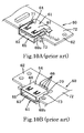
- Fig. 10 illustrates the connector set forth in this Japanese Patent Application Publication, Fig. 10A being a top view of the connector and Fig. 10B being a rear view thereof.
- a circuit module 60 is equipped with a USB connector 61 constituting a circuit component, and with a printed circuit board 62 to which the USB connector 61 is mounted.
- the USB connector 61 has a connector body 63 and a metallic shield cover 64 that covers the connector body 63.
- the connector body 63 has an insertion mouth 65 into which the plug of a USB cable is removably inserted, and multiple pin terminals 66.
- the insertion mouth 65 is formed at one end of the connector body 63.
- the pin terminals 66 are located at the opposite end to the insertion mouth 65, and are projected to the exterior of the connector body 63.
- the shield cover 64 has a top plate 67 that covers the connector body 63 from above, a bottom plate 68 that covers the connector body 63 from below, and left and right lateral plates 69a, 69b that cover the connector body 63 laterally. Further, the shield cover 64 takes the form of a flattened box having four sharply right-angled corners 70, these corners 70 being located on the peripheral surface of the USB connector 61.
- the lateral plates 69a, 69b of the shield cover 64 each have a conducting strip 71. The conducting strips 71 jut out to the sides of the shield cover 64 and are positioned on the printed circuit board 62.
- the printed circuit board 62 has an oblong substrate 72.
- the substrate 72 is formed by stacking insulating layers and conducting layers alternately, and applying pressure.
- the substrate 72 has a cut portion 73 which is formed by performing cutting or punch processing on the substrate 72.
- the cut portion 73 constitutes a recess that is formed so as to be open at the outer edge of the substrate 72 and is of a size such that the USB connector 61 will enter thereinto.
- a USB connector such as mentioned here is disclosed in JP-A-11-260489 .
- USB connectors of this kind are fixed to a printed circuit board by means of solder connections, and therefore, once fixed to the board, cannot be removed therefrom unless the solder is melted. This means that repair or replacement, etc., of the connector is not a simple matter.
- solder connections are fixed to a printed circuit board by means of solder connections, and therefore, once fixed to the board, cannot be removed therefrom unless the solder is melted.
- repair or replacement, etc., of the connector is not a simple matter.
- practices have arisen such as the use of solder that does not contain lead, and of what are termed "solderless" connections that do not use solder, these practices have the implicit issue of not being able to address the foregoing problems with this type of connector. Accordingly, in order to resolve such issues, connectors that can be connected to circuit boards without using solder have been developed. Examples of such connectors are those disclosed in JP-A-11-242971 and JP-A-7-245147 issued in Japan.
- USB connector disclosed in JP-A-2003-347685 is, as mentioned above, fixed to a circuit board by means of solder connections, and therefore, once fixed to the board, cannot be removed therefrom unless the solder is melted. This means that repair and replacement, etc., of this connector is not a simple matter.
- connectors such as disclosed in JP-A-11-242971 and JP-A-7-245147 do not require soldering. Nevertheless, in order to remove connector housings thereof from the circuit board, one must be unfasten such from the board by using a tool or the like at the reverse surface of the board. Thus, removal thereof is not a simple matter either. Further, these connectors are not shielded, and therefore are susceptible to the effects of external noise.
- An advantage of some aspects of the present invention is to provide an electric connector that has an attaching means enabling not only simple attachment to a board, but also simple removal therefrom.
- Another advantage is to provide an electric connector that is shielded and suitable as a USB connector.
- Another advantage is to provide an electric connector that has a low number of components and is simple to assemble, besides also being compact and low-cost.
- an electric connector includes a contact terminal, and a connector housing in which the contact terminal is installed, and has the advantageous features that the connector housing has a supporting base with front and rear surfaces of a particular size, a pair of arm parts of a particular length that extend outward, with a particular spacing therebetween, from the two ends of either the front or the rear surface of the supporting base, and a terminal attachment part to which the contact terminal is installed and which extends outward from a central portion of the other surface, front or rear, of the supporting base.
- the contact terminal is installed to the terminal attachment part, at each tip of the pair of arm parts there is provided a latching part with release finger which is detachably attached to a board to which the connector is installed; and the whole connector housing is formed as one integral molding.
- the connector housing is provided with latching parts with release fingers, and by manipulating the release fingers, the connector can be installed to and removed from a circuit board in a simple manner.
- the connector housing being so configured that the latching parts with release fingers project from one surface of the supporting base, and the terminal attachment part from another surface, has therefore a simple structure, is easy to mold, and can be manufactured at low cost.
- Embodiments of the present invention can therefore provide an electric connector, and more particularly an electric connector that has an attaching means enabling installation and removal in a simple manner to and from a printed circuit board, and which can be connected especially well to a plug connected to a USB cable.
- the latching parts with release fingers may be formed with the release fingers extending from the tips of the arm parts in one direction orthogonal to the longitudinal direction of the arm parts, and likewise with latching pieces extending from the tips of the arm parts in the other direction orthogonal to the longitudinal direction of the arm parts.
- the latching parts with release fingers can be formed on the connector housing in a simple manner.
- projections that will serve as rocking fulcrums will preferably be provided in the proximity of the boundary between the release fingers and the latching pieces.
- the projections serving as rocking fulcrums are provided in the proximity of the boundary between the release fingers and the latching pieces, so that when the pair of release fingers are brought closer together in order to remove the connector from the circuit board, the actuation motions of the latching pieces are centered on these projections, and thus the connector can be removed in a simple manner.
- the contact terminal may have a contacting portion at both ends, and may be so installed to the terminal attachment part that one contacting portion is positioned at the terminal attachment part and the other contacting portion is positioned beyond the supporting base, between the pair of arm parts.
- the contact terminal can be connected to the contacting portions of the circuit board without using solder.
- the terminal attachment part may preferably be covered by a shield cover that has a plug insertion mouth at one end.
- the terminal attachment part is covered by a shield cover with a plug insertion mouth at one end, and thereby the penetration of external noise will be prevented.
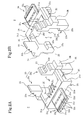
- FIG. 1 is an exploded perspective view of an electric connector in an embodiment of the invention
- Fig. 2 illustrates the housing of the electric connector in Fig. 1
- Fig. 2A being a perspective view thereof from one direction
- Fig. 2B a perspective view thereof from another direction
- Fig. 3 illustrates the assembled electric connector
- Fig. 3A being a top view thereof
- Fig. 3B a front view
- Fig. 3C a rear view
- Fig. 3D a side view.
- An electric connector 1 has multiple contact terminals 3, a connector housing 2 (hereinafter simply referred to as the "housing") in which the contact terminals 3 are installed, and a shield cover 4 that covers the contact terminals 3 installed inside the housing 2. Also, the housing 2 is provided with a terminal attachment part 2B for attachment of the contact terminals 3, and a pair of latching parts 2D 1 , 2D 1 with release fingers which are detachably attached to a printed circuit board 5. The structure of each of these members is described individually below.
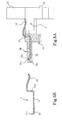
- the multiple contact terminals 3 all have the same shape and are formed by bend-processing strip-form pieces of a plate material with good conductivity. As shown in Figs. 1 and 5A , these contact terminals 3 are elongated strip-form pieces 31 provided with contacting portions 32, 33 at either end. Also, the strip-form piece 31 has a latching part 31a formed at one end, and is provided with a bend portion 31b midway along its length. Of the contacting portions 32, 33, the contacting portion 32 is connected to a plug (omitted from the drawings) and the other contacting portion 33 is connected to a contact 54 on the printed circuit board 5.
- the housing 2 has, as shown in Fig. 2 , a supporting base 2A located roughly in the center thereof, a terminal attachment part 2B to which the multiple contact terminals 3 are installed and which projects a particular distance outward from one side of the supporting base 2A, a pair of arm parts 2C, 2C that project a particular distance outward from the two longitudinal ends of the other side, and hand parts 2D, 2D provided on the tips of the arm parts 2C, 2C. Further, latching parts 2D 1 , 2D 1 with release fingers are provided on the hand parts 2D, 2D. Also, the housing 2 is formed as a single integral molding of electrically insulative synthetic resin.
- the supporting base 2A is formed as a plate-form body having particular width, length and thickness. Such plate-form body will be formed to the desired size according to the connector size.
- This supporting base 2A has top, bottom, left and right wall surfaces 21a, 21 b, 21 c, 21 d, as well as front and rear wall surfaces 21 e, 21 f.
- In the top wall surface 21 a there are formed multiple insertion holes 21 1 through which the bend portions 31b of the contact terminals 3 are inserted.
- the terminal attachment part 2B is formed as a plate-form body having particular width, length and thickness. The size of such plate-form body will be determined according to the size of the connector to which the electric connector 1 is connected, and the number of contact terminals 3 installed therein.
- This terminal attachment part 2B has top, bottom, left and right wall surfaces 22a, 22b, 22c, 22d, and one edge thereof is integrally joined to the front wall surface 21e of the supporting base 2A.
- In the bottom wall surface 22b there are formed multiple flat-bottomed grooves 22 1 into which the contact terminals 3 are fitted.
- latching holes 22 2 that penetrate from the top wall surface 22a through to the bottom wall surface 22b.
- the flat-bottomed grooves 22 1 communicate with the insertion holes 21 1 at one end, and at the other end communicate with the latching holes 22 2 .
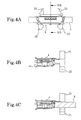
- Fig. 4 explicates the installation of the electric connector to the printed circuit board, Fig. 4A being a front view of the connector, Fig. 4B a cross-sectional view along line IVB - IVB in Fig. 4A, and Fig. 4C a cross-sectional view corresponding to that in Fig. 4B but prior to installation to the printed circuit board.
- Fig. 5 explicates the contact terminal, Fig. 5A being a side view of the contact terminal, and Fig. 5B a cross-sectional view of the contact terminal of Fig. 5A installed in the housing.
- the multiple contact terminals 3 are inserted into and fixed in the flat-bottomed grooves 22 1 in the terminal attachment part 2B.
- Such fixing operation is performed by inserting the strip-form pieces 31 of the contact terminals 3 into the flat-bottomed grooves 22 1 , inserting the bend portions 31b through the insertion holes 21 1 , and inserting the latching parts 31 a into the latching holes 22 2 so as to latch thereto.
- the contacting portions 32 at one end are positioned inside the flat-bottomed grooves 22 1 , and the contacting portions 33 at the other end are projected into the space S between the pair of arm parts 2C, 2C.
- each arm part 2C has a particular thickness, and projects almost perpendicularly from the rear wall surface 21 f of the supporting base 2A.
- the portions where the arm parts 2C, 2C join with the supporting base 2A are made thick, and high mechanical strength is thereby imparted thereto.
- the arm parts 2C, 2C oppose each other, approximately in parallel, and a space S is formed therebetween. Into this space S, the protrusion 52 in the printed circuit board 5 is inserted.
- the release fingers 23, 23 are formed as relatively long pieces having the same shape. Multiple step portions 23a, 23a are formed, stair-like, on the outside of each release finger 23, 23. Also, the spacing between the two release fingers 23, 23 is smaller than the width of the protrusion 52 in the printed circuit board 5. Thereby, when the electric connector 1 is installed to the printed circuit board 5, the inner bottom parts of the release fingers 23, 23 will rest on the top surface of the protrusion 52 in the printed circuit board 5, and good positioning will be effected. Also, since the release fingers 23, 23 are relatively long, it is easy to take hold thereof. Thus when one takes hold, with one's fingers, of the apexes of the release fingers 23, 23 and pushes them closer together, the latching pieces 25, 25 will open outward, with the projections 24, 24 serving as rocking fulcrums therefor.
- the pair of latching pieces 25, 25 have the same shape. At the mutually opposed faces of the end portions of the latching pieces 25, 25 there are formed latching ledges 25a, 25a. Below the latching ledges 25a, 25a, at the tips, there are provided inclined portions 25b, 25b facilitating installation into the latching openings in the printed circuit board 5.
- the shield cover 4 is fitted over the terminal attachment part 2B.
- the shield cover 4 is constituted of a flattened tubular body, whose periphery is enclosed by top, bottom and lateral plates 41a to 41d, which has a through-hole in the interior, and which is formed by bend-processing of metal plate.
- the rear opening 41 2 has outer dimensions of roughly the same size as the supporting base 2A, while the front opening 41 1 is of a size enabling insertion of a USB plug not shown in the drawings.
- conductive pieces 42, 42 are formed in the lateral plates 41 c, 41 d.
- the rear opening 41 2 is provided with attachment pieces 43, 43 at the rim thereof.
- the electric connector 1 is assembled by installing the contact terminals 3 to the terminal attachment part 2B, placing the shield cover 4 over the terminal attachment part 2B, and making the attachment pieces 43, 43 of the shield cover latch to the arm parts 2C, 2C.
- this electric connector 1 is both simple to manufacture and simple to assemble.
- This attaching slot 51 has, in the interior thereof, which is of a particular size, a protrusion 52 of a size such as to be inserted onto the space S of the housing 2, and at the two sides of the protrusion 52, a pair of latching apertures 53, 53 into which the pair of latching pieces 25, 25 are inserted.
- the latching apertures 53, 53 are of a size enabling insertion of the projections 24, 24 thereinto.
- Fig. 6 is a perspective view of the printed circuit board and electric connector prior to installation.
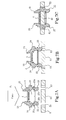
- Fig. 7 explicates the process of installing the electric connector to the printed circuit board, being a series of cross-sectional views along line VII - VII in Fig. 6
- Fig. 8 is a perspective view of the printed circuit board and electric connector midway through installation
- Fig. 9 explicates the process of removing the electric connector from the printed circuit board, being a series of cross-sectional views along line IX - IX in Fig. 8 .
- the electric connector 1 To install the electric connector 1 to the printed circuit board 5, first of all, the electric connector 1 is moved to above the printed circuit board 5 so as to position the pair of latching pieces 25, 25 over the latching apertures 53, 53 in the printed circuit board 5, as shown in Figs. 6 and 7 . With such state, the electric connector 1 is made to descend from above by application of a particular push force P1, so that the tips of the latching pieces 25, 25 are inserted into the latching apertures 53, 53 (see Fig. 7A ).
- the latching ledges 25a, 25a of the latching pieces 25, 25 are latched onto the reverse surface of the printed circuit board 5, whereupon installation of the electric connector 1 to the printed circuit board 5 is complete.
- the electric connector can be installed in a simple manner, just by being pushed onto the printed circuit board 5. Also, this will effect electrical connection between the contacting portions 33 of the contact terminals 3 and the contacts 54 on the printed circuit board 5. Such connection will be effected without using solder.
Landscapes
- Coupling Device And Connection With Printed Circuit (AREA)
- Details Of Connecting Devices For Male And Female Coupling (AREA)
Applications Claiming Priority (1)
| Application Number | Priority Date | Filing Date | Title |
|---|---|---|---|
| SG200708379-3A SG151115A1 (en) | 2007-09-21 | 2007-09-21 | Electric connector |
Publications (2)
| Publication Number | Publication Date |
|---|---|
| EP2040338A2 true EP2040338A2 (fr) | 2009-03-25 |
| EP2040338A3 EP2040338A3 (fr) | 2010-01-13 |
Family
ID=40191602
Family Applications (1)
| Application Number | Title | Priority Date | Filing Date |
|---|---|---|---|
| EP08253081A Withdrawn EP2040338A3 (fr) | 2007-09-21 | 2008-09-19 | Connecteur électrique |
Country Status (5)
| Country | Link |
|---|---|
| US (1) | US20090081900A1 (fr) |
| EP (1) | EP2040338A3 (fr) |
| JP (1) | JP2009076454A (fr) |
| CN (1) | CN101394048A (fr) |
| SG (1) | SG151115A1 (fr) |
Cited By (2)
| Publication number | Priority date | Publication date | Assignee | Title |
|---|---|---|---|---|
| CN105048202A (zh) * | 2015-08-07 | 2015-11-11 | 连展科技(深圳)有限公司 | 直立型插座电连接器 |
| CN106684593A (zh) * | 2017-01-18 | 2017-05-17 | 启东乾朔电子有限公司 | 插座连接器 |
Families Citing this family (7)
| Publication number | Priority date | Publication date | Assignee | Title |
|---|---|---|---|---|
| CN101924287B (zh) * | 2009-08-05 | 2014-03-12 | 安费诺东亚电子科技(深圳)有限公司 | 铡刀式连接器 |
| KR101569842B1 (ko) * | 2009-09-30 | 2015-11-17 | 삼성전자 주식회사 | 텔레비전용 전원공급유닛 및 이를 포함하는 텔레비전 |
| CN201656090U (zh) | 2010-03-29 | 2010-11-24 | 美国莫列斯股份有限公司 | 电连接器 |
| CN102280781A (zh) * | 2010-06-08 | 2011-12-14 | 祥峰实业股份有限公司 | 连接器结构 |
| TWM432999U (en) * | 2011-11-16 | 2012-07-01 | Innostor Tech Corporation | Circuit board and a storage device using the circuit board |
| JP7046453B2 (ja) * | 2018-12-27 | 2022-04-04 | 株式会社クボタ | 作業車 |
| CN110459889B (zh) * | 2019-08-14 | 2021-02-02 | 东莞市信为兴电子有限公司 | 一种type-c连接器 |
Citations (4)
| Publication number | Priority date | Publication date | Assignee | Title |
|---|---|---|---|---|
| JPH07245147A (ja) | 1994-03-02 | 1995-09-19 | Hosiden Corp | モジュラージャック |
| JPH11242971A (ja) | 1998-02-25 | 1999-09-07 | Iriso Denshi Kogyo Kk | 電気コネクタ及びその基板接続構造 |
| JPH11260489A (ja) | 1997-12-30 | 1999-09-24 | Whitaker Corp:The | Lan用電気コネクタ |
| JP2003347685A (ja) | 2002-05-24 | 2003-12-05 | Toshiba Corp | プリント配線板、回路モジュールおよびプリント配線板の製造方法 |
Family Cites Families (13)
| Publication number | Priority date | Publication date | Assignee | Title |
|---|---|---|---|---|
| US5310360A (en) * | 1993-05-18 | 1994-05-10 | Molex Incorporated | Circuit board mounted modular phone jack |
| US5690513A (en) * | 1995-11-17 | 1997-11-25 | General Motors Corporation | Header connector snap lock |
| US6165015A (en) * | 1997-07-17 | 2000-12-26 | Hon Hai Precision Ind. Co., Ltd. | Electrical connector |
| DE10037908B4 (de) * | 1999-08-05 | 2010-11-25 | The Whitaker Corp., Wilmington | Anordnung zum Verbinden eines Gehäuses mit einer Platte und Steckverbinder zur Montage auf einer Platte |
| US6371771B1 (en) * | 2000-12-28 | 2002-04-16 | Hon Hai Precision Ind. Co., Ltd. | Universal serial bus connector with power transmission function |
| JP4767450B2 (ja) * | 2001-08-09 | 2011-09-07 | ポリマテック株式会社 | コネクタおよびその製造方法 |
| JP4201505B2 (ja) * | 2001-12-28 | 2008-12-24 | 日本圧着端子製造株式会社 | パネル取付用係止部材を備えたコネクタ及びこのコネクタのパネルへの取付方法並びに他のコネクタへの結合方法 |
| US6767224B2 (en) * | 2002-08-08 | 2004-07-27 | Hon Hai Precision Ind. Co., Ltd. | Electrical connector with improved terminal retaining system |
| JP2005101088A (ja) * | 2003-09-22 | 2005-04-14 | Aisin Seiki Co Ltd | 固定部材 |
| TWM260892U (en) * | 2004-08-13 | 2005-04-01 | Advanced Connectek Inc | Electrical connector |
| TWM293569U (en) * | 2005-11-25 | 2006-07-01 | Advanced Connectek Inc | Universal serial connector |
| US7473132B2 (en) * | 2006-08-04 | 2009-01-06 | Advanced Connectek Inc. | IEEE 1394 electrical connector |
| US7465193B2 (en) * | 2007-04-05 | 2008-12-16 | Cheng Uei Precision Industry Co., Ltd. | Shielded surface mount connector |
-
2007
- 2007-09-21 SG SG200708379-3A patent/SG151115A1/en unknown
-
2008
- 2008-08-27 JP JP2008217908A patent/JP2009076454A/ja active Pending
- 2008-09-09 US US12/230,969 patent/US20090081900A1/en not_active Abandoned
- 2008-09-17 CN CNA2008101489306A patent/CN101394048A/zh active Pending
- 2008-09-19 EP EP08253081A patent/EP2040338A3/fr not_active Withdrawn
Patent Citations (4)
| Publication number | Priority date | Publication date | Assignee | Title |
|---|---|---|---|---|
| JPH07245147A (ja) | 1994-03-02 | 1995-09-19 | Hosiden Corp | モジュラージャック |
| JPH11260489A (ja) | 1997-12-30 | 1999-09-24 | Whitaker Corp:The | Lan用電気コネクタ |
| JPH11242971A (ja) | 1998-02-25 | 1999-09-07 | Iriso Denshi Kogyo Kk | 電気コネクタ及びその基板接続構造 |
| JP2003347685A (ja) | 2002-05-24 | 2003-12-05 | Toshiba Corp | プリント配線板、回路モジュールおよびプリント配線板の製造方法 |
Cited By (2)
| Publication number | Priority date | Publication date | Assignee | Title |
|---|---|---|---|---|
| CN105048202A (zh) * | 2015-08-07 | 2015-11-11 | 连展科技(深圳)有限公司 | 直立型插座电连接器 |
| CN106684593A (zh) * | 2017-01-18 | 2017-05-17 | 启东乾朔电子有限公司 | 插座连接器 |
Also Published As
| Publication number | Publication date |
|---|---|
| SG151115A1 (en) | 2009-04-30 |
| US20090081900A1 (en) | 2009-03-26 |
| CN101394048A (zh) | 2009-03-25 |
| EP2040338A3 (fr) | 2010-01-13 |
| JP2009076454A (ja) | 2009-04-09 |
Similar Documents
| Publication | Publication Date | Title |
|---|---|---|
| EP2040338A2 (fr) | Connecteur électrique | |
| US10756466B2 (en) | Connector | |
| KR101832599B1 (ko) | 커넥터 | |
| CN103311718B (zh) | 连接器 | |
| US8308492B2 (en) | Board-to-board connector | |
| US8113884B2 (en) | Connector | |
| JP7536724B2 (ja) | コネクタ及びコネクタ対 | |
| JP5197294B2 (ja) | 基板対基板コネクタ | |
| WO2005096456A1 (fr) | Connecteur | |
| CN1983737A (zh) | 插座型连接器和插头型连接器 | |
| US7097466B2 (en) | Electronic part-mounting socket | |
| US6599140B1 (en) | Electrical connector assembly having a placement member | |
| WO2008109044A2 (fr) | Ensemble de borne et connecteur de câbles plats | |
| US20060121782A1 (en) | Electrical connector having an improved grounding path | |
| KR101452626B1 (ko) | 회로기판 수직 접속용 커넥터 조립체 | |
| CN104253345A (zh) | 连接器以及在该连接器中使用的插头件及插口件 | |
| CN104979709A (zh) | 基板对基板用连接器 | |
| CN103403973A (zh) | 连接器端子及包含该连接器端子的卡缘型连接器 | |
| CN205178054U (zh) | 卡用连接器 | |
| JP2023001183A (ja) | 金具、金具付きコネクタ及びコネクタ組立体 | |
| KR101378702B1 (ko) | 전기 커넥터 | |
| JP2006012886A (ja) | シールド構造 | |
| WO2008047482A1 (fr) | Connecteur | |
| JP2023183819A (ja) | コネクタ及びコネクタ対 | |
| JP4498890B2 (ja) | 一対のヘッダーコンタクト及びこれを用いたヘッダーコネクタ |
Legal Events
| Date | Code | Title | Description |
|---|---|---|---|
| PUAI | Public reference made under article 153(3) epc to a published international application that has entered the european phase |
Free format text: ORIGINAL CODE: 0009012 |
|
| AK | Designated contracting states |
Kind code of ref document: A2 Designated state(s): AT BE BG CH CY CZ DE DK EE ES FI FR GB GR HR HU IE IS IT LI LT LU LV MC MT NL NO PL PT RO SE SI SK TR |
|
| AX | Request for extension of the european patent |
Extension state: AL BA MK RS |
|
| PUAL | Search report despatched |
Free format text: ORIGINAL CODE: 0009013 |
|
| AK | Designated contracting states |
Kind code of ref document: A3 Designated state(s): AT BE BG CH CY CZ DE DK EE ES FI FR GB GR HR HU IE IS IT LI LT LU LV MC MT NL NO PL PT RO SE SI SK TR |
|
| AX | Request for extension of the european patent |
Extension state: AL BA MK RS |
|
| AKY | No designation fees paid | ||
| REG | Reference to a national code |
Ref country code: DE Ref legal event code: 8566 |
|
| STAA | Information on the status of an ep patent application or granted ep patent |
Free format text: STATUS: THE APPLICATION IS DEEMED TO BE WITHDRAWN |
|
| 18D | Application deemed to be withdrawn |
Effective date: 20100714 |