EP2040344A2 - Dispositif de commutation destiné au fonctionnement d'une diode laser à impulsions et procédé de fonctionnement d'une diode laser à impulsions - Google Patents
Dispositif de commutation destiné au fonctionnement d'une diode laser à impulsions et procédé de fonctionnement d'une diode laser à impulsions Download PDFInfo
- Publication number
- EP2040344A2 EP2040344A2 EP08162321A EP08162321A EP2040344A2 EP 2040344 A2 EP2040344 A2 EP 2040344A2 EP 08162321 A EP08162321 A EP 08162321A EP 08162321 A EP08162321 A EP 08162321A EP 2040344 A2 EP2040344 A2 EP 2040344A2
- Authority
- EP
- European Patent Office
- Prior art keywords
- laser diode
- pulse laser
- current
- operating
- temperature
- Prior art date
- Legal status (The legal status is an assumption and is not a legal conclusion. Google has not performed a legal analysis and makes no representation as to the accuracy of the status listed.)
- Granted
Links
Images


Classifications
-
- H—ELECTRICITY
- H01—ELECTRIC ELEMENTS
- H01S—DEVICES USING THE PROCESS OF LIGHT AMPLIFICATION BY STIMULATED EMISSION OF RADIATION [LASER] TO AMPLIFY OR GENERATE LIGHT; DEVICES USING STIMULATED EMISSION OF ELECTROMAGNETIC RADIATION IN WAVE RANGES OTHER THAN OPTICAL
- H01S5/00—Semiconductor lasers
- H01S5/04—Processes or apparatus for excitation, e.g. pumping, e.g. by electron beams
- H01S5/042—Electrical excitation ; Circuits therefor
-
- H—ELECTRICITY
- H01—ELECTRIC ELEMENTS
- H01S—DEVICES USING THE PROCESS OF LIGHT AMPLIFICATION BY STIMULATED EMISSION OF RADIATION [LASER] TO AMPLIFY OR GENERATE LIGHT; DEVICES USING STIMULATED EMISSION OF ELECTROMAGNETIC RADIATION IN WAVE RANGES OTHER THAN OPTICAL
- H01S5/00—Semiconductor lasers
- H01S5/04—Processes or apparatus for excitation, e.g. pumping, e.g. by electron beams
- H01S5/042—Electrical excitation ; Circuits therefor
- H01S5/0428—Electrical excitation ; Circuits therefor for applying pulses to the laser
-
- H—ELECTRICITY
- H01—ELECTRIC ELEMENTS
- H01S—DEVICES USING THE PROCESS OF LIGHT AMPLIFICATION BY STIMULATED EMISSION OF RADIATION [LASER] TO AMPLIFY OR GENERATE LIGHT; DEVICES USING STIMULATED EMISSION OF ELECTROMAGNETIC RADIATION IN WAVE RANGES OTHER THAN OPTICAL
- H01S5/00—Semiconductor lasers
- H01S5/06—Arrangements for controlling the laser output parameters, e.g. by operating on the active medium
- H01S5/062—Arrangements for controlling the laser output parameters, e.g. by operating on the active medium by varying the potential of the electrodes
- H01S5/06209—Arrangements for controlling the laser output parameters, e.g. by operating on the active medium by varying the potential of the electrodes in single-section lasers
- H01S5/06216—Pulse modulation or generation
-
- H—ELECTRICITY
- H01—ELECTRIC ELEMENTS
- H01S—DEVICES USING THE PROCESS OF LIGHT AMPLIFICATION BY STIMULATED EMISSION OF RADIATION [LASER] TO AMPLIFY OR GENERATE LIGHT; DEVICES USING STIMULATED EMISSION OF ELECTROMAGNETIC RADIATION IN WAVE RANGES OTHER THAN OPTICAL
- H01S5/00—Semiconductor lasers
- H01S5/06—Arrangements for controlling the laser output parameters, e.g. by operating on the active medium
- H01S5/062—Arrangements for controlling the laser output parameters, e.g. by operating on the active medium by varying the potential of the electrodes
- H01S5/06209—Arrangements for controlling the laser output parameters, e.g. by operating on the active medium by varying the potential of the electrodes in single-section lasers
- H01S5/0622—Controlling the frequency of the radiation
-
- H—ELECTRICITY
- H01—ELECTRIC ELEMENTS
- H01S—DEVICES USING THE PROCESS OF LIGHT AMPLIFICATION BY STIMULATED EMISSION OF RADIATION [LASER] TO AMPLIFY OR GENERATE LIGHT; DEVICES USING STIMULATED EMISSION OF ELECTROMAGNETIC RADIATION IN WAVE RANGES OTHER THAN OPTICAL
- H01S5/00—Semiconductor lasers
- H01S5/06—Arrangements for controlling the laser output parameters, e.g. by operating on the active medium
- H01S5/068—Stabilisation of laser output parameters
- H01S5/0683—Stabilisation of laser output parameters by monitoring the optical output parameters
- H01S5/06837—Stabilising otherwise than by an applied electric field or current, e.g. by controlling the temperature
-
- H—ELECTRICITY
- H01—ELECTRIC ELEMENTS
- H01S—DEVICES USING THE PROCESS OF LIGHT AMPLIFICATION BY STIMULATED EMISSION OF RADIATION [LASER] TO AMPLIFY OR GENERATE LIGHT; DEVICES USING STIMULATED EMISSION OF ELECTROMAGNETIC RADIATION IN WAVE RANGES OTHER THAN OPTICAL
- H01S5/00—Semiconductor lasers
- H01S5/06—Arrangements for controlling the laser output parameters, e.g. by operating on the active medium
- H01S5/068—Stabilisation of laser output parameters
- H01S5/0683—Stabilisation of laser output parameters by monitoring the optical output parameters
- H01S5/0687—Stabilising the frequency of the laser
Definitions
- the invention relates to a circuit arrangement for operating a pulse laser diode, wherein the pulse laser diode is supplied with power. Moreover, the invention also relates to a method for operating the pulse laser diode.
- a device having a radiation-emitting semiconductor component, wherein the semiconductor component is assigned at least one electrical heating element, is known from the document DE 10 2005 004 145 A1 known.
- An object to be solved is to provide a circuit arrangement for operating a pulse laser diode, by means of which a pulse laser diode can be operated as stable as possible.
- the invention relates to a circuit arrangement for operating a pulse laser diode, which comprises a pulse laser diode.
- a current source is provided which is suitable for feeding a direct current into the pulse laser diode.
- the temperature of the chip of the laser diode can be influenced. This allows the temperature to be controlled within certain limits.
- a means which serves to limit the current fed into the pulse laser diode.
- the current is limited to a value which is smaller than the laser threshold of the pulse laser diode.
- the influence on the temperature of the pulse laser diode has the advantage that the temperature can be kept within certain limits using suitable further means which are described below. As a result, an uncontrolled and unintentional drifting of the temperature of the pulse laser diode can be prevented. It can thus be achieved that the pulse wave length at which the pulse laser diode emits its radiation can be kept stable within certain limits.
- pulsed laser diodes are preferably used in the circuit arrangement whose peak wavelength of the emitted radiation is dependent on the temperature of the chip of the pulse laser diode.
- pulse laser diodes can be used whose emission wavelength or pulse wavelength per Kelvin temperature difference changes by +0.3 nm.
- the pulse laser diode This allows the use of the pulse laser diode, especially in automotive applications, where they are used in sensors for distance measurement.
- the receiver of the light emitted by the pulse laser diode can always operate in a good or even always at the optimum operating point.
- pulse laser diode described here together with the associated circuitry allows the use of narrow-band filters in front of the receiver or detector, which environmental or disturbance light can be suppressed very well and thus at the same time the ratio of signal-to-noise high can be held.
- the current source is suitable for feeding a current into the diode which is sufficient to increase the temperature in the chip of the diode by at least 10 K.
- a measuring device is included in the circuit arrangement which is used to determine the temperature of the pulse laser diode is provided.
- the temperature of the pulse laser diode can be controlled with the suitable choice of a current source, which can be used, for example, to keep the temperature of the pulsed laser diode and thus the peak wavelength of the light emitted by the pulse laser diode as constant as possible.
- the measuring device is coupled to the current source, wherein the current fed into the pulse laser diode current can be controlled by an electrical signal.
- the control of the current fed into the pulse laser diode is effected by a signal which depends on the measured temperature of the pulse laser diode.
- a method for operating a pulse laser diode wherein a direct current is fed into the pulse laser diode to adjust its temperature to a predetermined value.
- Such a method can be carried out, for example, by means of the circuit arrangement described here.
- the temperature of the pulse laser diode is kept constant by means of a suitable control device.
- pulse wave length of the pulse laser diode is controlled by the injection of a direct current into the pulse laser diode.
- the temperature of the pulse laser diode can be adjusted by the level of the direct current, since the temperature of the pulsed laser diode also increases with the current fed in.
- the current fed in is kept constant in order to heat the pulse laser diode and keep it at a constant temperature, regardless of how the external temperature develops in the environment.
- FIG. 1 shows a circuit arrangement for operating a pulse laser diode, wherein a pulse laser diode 1 is provided. To operate the pulse laser diode, a pulser circuit 5 is used. In the in FIG. 1 In the embodiment shown, the pulse laser diode is the model SPL PL90.
- the pulser circuit is designed so that it can feed a current of 30 A into the pulse laser diode 1.
- the current pulses have a pulse duration of 100 ns and are fed into the pulse laser diode 1 at a frequency of 1 kHz.
- a DC power source 2 which feeds a direct current into the pulse laser diode 1.
- the direct current preferably flows through a current limiting means 3, which may be, for example, an ohmic resistor.
- a resistance of 100 ⁇ In the example of FIG. 1 is used as current limit 3, a resistance of 100 ⁇ .
- the current source in the example of FIG. 1 delivers one Supply voltage between 0 V and 16.5 V, resulting in a resistance of 100 ⁇ to a DC current of between 0 and 150 mA, which flows via the current source 2, the current limit 3, the laser diode 1 finally to the ground terminal 6.
- a temperature measuring device 4 is provided, which may be coupled to the power source, for example by means of an electrical line.
- the measured values relating to the temperature of the pulse laser diode 1 supplied by the temperature measuring device 4 can be used to control the current source 2.
- FIG. 2 shows the in an arrangement after FIG. 1 measured optical intensity of the pulse laser diode as a function of the wavelength ⁇ of the light emitted by the laser diode for different direct currents, which are fed into the pulse laser diode.
- the curve 10 shows the optical intensity I as a function of the wavelength ⁇ for a direct current of 0 mA.
- the curve 11 shows the intensity for a direct current of 30 mA.
- the curve 12 shows the intensity for a direct current of 60 mA.
- the curve 13 shows the intensity for a direct current of 90 mA.
- Curve 14 shows the intensity for a direct current of 120 mA.
- the curve 15 shows the intensity for a direct current of 150 mA.
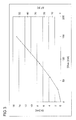
- FIG. 3 shows the change of the pulse wave length, as in FIG. 2 is shown, depending on the injected DC.
- FIG. 3 shows FIG. 3 the change in the temperature ⁇ T as a function of the injected direct current IBIAS.
- FIG. 3 It can be seen that at least from an injected current of about 50 mA, a nearly proportional relationship between the injected DC and the wavelength change ⁇ on the one hand and the injected DC IBIAS and the temperature change .DELTA.T on the other hand prevails. This shows that the control of the wavelength of the emitted light and the control of the temperature of the pulsed laser diode is very easy and possible without much circuit or computational effort.
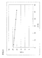
- FIG. 4 shows the dependence of the optical power P of the pulse laser diode in response to the temperature increase .DELTA.T the pulse laser diode.
- results in a linear relationship with a rise of -0.08 W / K, a very low dependence of the optical power of the temperature increase is detected. This shows that the operation of a pulse laser diode at elevated temperature is very stable and without major losses in terms of optical power P is possible.
Landscapes
- Physics & Mathematics (AREA)
- Condensed Matter Physics & Semiconductors (AREA)
- General Physics & Mathematics (AREA)
- Electromagnetism (AREA)
- Optics & Photonics (AREA)
- Semiconductor Lasers (AREA)
Applications Claiming Priority (1)
| Application Number | Priority Date | Filing Date | Title |
|---|---|---|---|
| DE102007044438A DE102007044438A1 (de) | 2007-09-18 | 2007-09-18 | Schaltungsanordnung zum Betrieb einer Pulslaserdiode und Verfahren zum Betrieb einer Pulslaserdiode |
Publications (3)
| Publication Number | Publication Date |
|---|---|
| EP2040344A2 true EP2040344A2 (fr) | 2009-03-25 |
| EP2040344A3 EP2040344A3 (fr) | 2010-12-29 |
| EP2040344B1 EP2040344B1 (fr) | 2015-05-20 |
Family
ID=39769605
Family Applications (1)
| Application Number | Title | Priority Date | Filing Date |
|---|---|---|---|
| EP20080162321 Active EP2040344B1 (fr) | 2007-09-18 | 2008-08-13 | Dispositif de commutation destiné au fonctionnement d'une diode laser à impulsions et procédé de fonctionnement d'une diode laser à impulsions |
Country Status (4)
| Country | Link |
|---|---|
| US (1) | US8094694B2 (fr) |
| EP (1) | EP2040344B1 (fr) |
| JP (1) | JP2009076913A (fr) |
| DE (1) | DE102007044438A1 (fr) |
Cited By (1)
| Publication number | Priority date | Publication date | Assignee | Title |
|---|---|---|---|---|
| CN102570306A (zh) * | 2011-12-31 | 2012-07-11 | 聚光科技(杭州)股份有限公司 | 连续激光器的驱动装置及方法 |
Families Citing this family (1)
| Publication number | Priority date | Publication date | Assignee | Title |
|---|---|---|---|---|
| US20120250707A1 (en) * | 2011-03-31 | 2012-10-04 | Electro Scientific Industries, Inc. | Stabilization of pulsed mode seed lasers |
Citations (9)
| Publication number | Priority date | Publication date | Assignee | Title |
|---|---|---|---|---|
| DE3005645A1 (de) | 1980-02-15 | 1981-08-20 | Licentia Patent-Verwaltungs-Gmbh, 6000 Frankfurt | Verfahren zur modulation eines halbleiterlasers |
| GB2224374A (en) | 1988-08-24 | 1990-05-02 | Plessey Co Plc | Temperature control of light-emitting devices |
| WO1993018563A1 (fr) | 1992-03-02 | 1993-09-16 | Ecrm Trust | Procede et appareil de stabilisation de l'emission d'energie d'une diode laser |
| US5400351A (en) | 1994-05-09 | 1995-03-21 | Lumonics Inc. | Control of a pumping diode laser |
| EP0957596A1 (fr) | 1994-06-30 | 1999-11-17 | AT&T Corp. | Générateur d'impulsions optiques à données codées |
| JP3283585B2 (ja) | 1992-09-07 | 2002-05-20 | 株式会社ソキア | Gps受信機 |
| US20050117616A1 (en) | 2001-11-28 | 2005-06-02 | Yukio Yamasaki | Nitride semiconductor laser device and semiconductor optical device |
| US20050199890A1 (en) | 2004-02-25 | 2005-09-15 | Osram Opto Semiconductors Gmbh | Device with a radiation-emitting semiconductor component and procedure for the temperature stabilization of a radiation-emitting semiconductor component |
| DE102005004145A1 (de) | 2004-02-25 | 2005-09-15 | Osram Opto Semiconductors Gmbh | Vorrichtung mit einem strahlungsemittierenden Halbleiterbauelement und Verfahren zur Temperaturstabilisierung eines strahlungsemittierenden Halbleiterbauelements |
Family Cites Families (4)
| Publication number | Priority date | Publication date | Assignee | Title |
|---|---|---|---|---|
| DE2542174C3 (de) * | 1974-09-21 | 1980-02-14 | Nippon Electric Co., Ltd., Tokio | Halbleiterlaservorrichtung |
| JPH03283585A (ja) * | 1990-03-30 | 1991-12-13 | Nec Corp | 光発振装置 |
| JP3628128B2 (ja) * | 1996-11-01 | 2005-03-09 | 富士写真フイルム株式会社 | 半導体発光素子の光量制御方法および装置 |
| JP2006066586A (ja) * | 2004-08-26 | 2006-03-09 | Oki Electric Ind Co Ltd | モード同期半導体レーザ装置及びモード同期半導体レーザ装置の波長制御方法 |
-
2007
- 2007-09-18 DE DE102007044438A patent/DE102007044438A1/de not_active Withdrawn
-
2008
- 2008-08-13 EP EP20080162321 patent/EP2040344B1/fr active Active
- 2008-09-17 US US12/211,939 patent/US8094694B2/en active Active
- 2008-09-18 JP JP2008240046A patent/JP2009076913A/ja active Pending
Patent Citations (9)
| Publication number | Priority date | Publication date | Assignee | Title |
|---|---|---|---|---|
| DE3005645A1 (de) | 1980-02-15 | 1981-08-20 | Licentia Patent-Verwaltungs-Gmbh, 6000 Frankfurt | Verfahren zur modulation eines halbleiterlasers |
| GB2224374A (en) | 1988-08-24 | 1990-05-02 | Plessey Co Plc | Temperature control of light-emitting devices |
| WO1993018563A1 (fr) | 1992-03-02 | 1993-09-16 | Ecrm Trust | Procede et appareil de stabilisation de l'emission d'energie d'une diode laser |
| JP3283585B2 (ja) | 1992-09-07 | 2002-05-20 | 株式会社ソキア | Gps受信機 |
| US5400351A (en) | 1994-05-09 | 1995-03-21 | Lumonics Inc. | Control of a pumping diode laser |
| EP0957596A1 (fr) | 1994-06-30 | 1999-11-17 | AT&T Corp. | Générateur d'impulsions optiques à données codées |
| US20050117616A1 (en) | 2001-11-28 | 2005-06-02 | Yukio Yamasaki | Nitride semiconductor laser device and semiconductor optical device |
| US20050199890A1 (en) | 2004-02-25 | 2005-09-15 | Osram Opto Semiconductors Gmbh | Device with a radiation-emitting semiconductor component and procedure for the temperature stabilization of a radiation-emitting semiconductor component |
| DE102005004145A1 (de) | 2004-02-25 | 2005-09-15 | Osram Opto Semiconductors Gmbh | Vorrichtung mit einem strahlungsemittierenden Halbleiterbauelement und Verfahren zur Temperaturstabilisierung eines strahlungsemittierenden Halbleiterbauelements |
Cited By (2)
| Publication number | Priority date | Publication date | Assignee | Title |
|---|---|---|---|---|
| CN102570306A (zh) * | 2011-12-31 | 2012-07-11 | 聚光科技(杭州)股份有限公司 | 连续激光器的驱动装置及方法 |
| CN102570306B (zh) * | 2011-12-31 | 2015-09-02 | 聚光科技(杭州)股份有限公司 | 连续激光器的驱动装置及方法 |
Also Published As
| Publication number | Publication date |
|---|---|
| JP2009076913A (ja) | 2009-04-09 |
| US8094694B2 (en) | 2012-01-10 |
| US20090074021A1 (en) | 2009-03-19 |
| EP2040344B1 (fr) | 2015-05-20 |
| DE102007044438A1 (de) | 2009-03-19 |
| EP2040344A3 (fr) | 2010-12-29 |
Similar Documents
| Publication | Publication Date | Title |
|---|---|---|
| DE3038538C2 (de) | Batterieladevorrichtung | |
| EP2123130B1 (fr) | Module d'activation et procédé de fonctionnement d'au moins un circuit de diodes électroluminescentes en série | |
| DE69618713T2 (de) | Schaltungsanordnung zur Ansteuerung von Laserdioden | |
| EP1936400B1 (fr) | Lecteur laser | |
| DE3331132C1 (de) | Schutzschaltung fuer einen Halbleiterlaser | |
| DE3210237A1 (de) | Laser-entfernungsmesser | |
| DE2847182B2 (de) | Verfahren zur Modulationsstromregelung von Laserdioden | |
| WO2020127013A1 (fr) | Dispositif pour faire fonctionner une source lumineuse servant à la mesure optique de temps de propagation | |
| EP2040344B1 (fr) | Dispositif de commutation destiné au fonctionnement d'une diode laser à impulsions et procédé de fonctionnement d'une diode laser à impulsions | |
| DE102015109373A1 (de) | Laufzeitverzögerungskompensation für einen floatenden abwärtswandler-leuchtdioden-(led)-treiber | |
| DE102017009551A1 (de) | Laserbearbeitungsvorrichtung | |
| EP2203977B1 (fr) | Circuit de protection d'un élément de commutation avec détection de surintensité de courant et d'élévation de température | |
| EP3159982A1 (fr) | Génération de impulsions laser avec forme stable | |
| DE102004006901B4 (de) | Näherungsschalter | |
| WO2009024504A1 (fr) | Source de lumière laser avec au moins deux lasers individuels | |
| DE102012022053B4 (de) | Schaltungsanordnung zum Betreiben einer Laserdiode | |
| DD243147A5 (de) | Verfahren und schaltungsanordnung zur bestimmung und regelung der temperatur von laserdioden | |
| EP4012460B1 (fr) | Procédé de fonctionnement d'un détecteur de rayonnement ainsi que détecteur de rayonnement | |
| DE102016007752B4 (de) | Schutzschaltung, Beleuchtungsanordnung und Betriebsverfahren | |
| AT503819A4 (de) | Verfahren und anordnung zur regelung der laser-pulsenergie | |
| DE102005028211B4 (de) | Schaltungsanordnung zum Verbinden eines ersten Schaltungsknotens mit einem zweiten Schaltungsknoten und zum Schutz des ersten Schaltungsknotens vor einer Überspannung | |
| EP3492951B1 (fr) | Dispositif optoélectronique | |
| EP3361282B1 (fr) | Capteur optique avec circuit limiteur | |
| DE102024110514B4 (de) | Pulserzeugungsvorrichtung, Treiberschaltung und Pulserzeugungsverfahren | |
| DE4323197A1 (de) | Verfahren und Anordnung zur Regelung von diodengepumpten Festkörperlasern |
Legal Events
| Date | Code | Title | Description |
|---|---|---|---|
| PUAI | Public reference made under article 153(3) epc to a published international application that has entered the european phase |
Free format text: ORIGINAL CODE: 0009012 |
|
| AK | Designated contracting states |
Kind code of ref document: A2 Designated state(s): AT BE BG CH CY CZ DE DK EE ES FI FR GB GR HR HU IE IS IT LI LT LU LV MC MT NL NO PL PT RO SE SI SK TR |
|
| AX | Request for extension of the european patent |
Extension state: AL BA MK RS |
|
| PUAL | Search report despatched |
Free format text: ORIGINAL CODE: 0009013 |
|
| AK | Designated contracting states |
Kind code of ref document: A3 Designated state(s): AT BE BG CH CY CZ DE DK EE ES FI FR GB GR HR HU IE IS IT LI LT LU LV MC MT NL NO PL PT RO SE SI SK TR |
|
| AX | Request for extension of the european patent |
Extension state: AL BA MK RS |
|
| 17P | Request for examination filed |
Effective date: 20110531 |
|
| AKX | Designation fees paid |
Designated state(s): DE FR GB |
|
| GRAP | Despatch of communication of intention to grant a patent |
Free format text: ORIGINAL CODE: EPIDOSNIGR1 |
|
| INTG | Intention to grant announced |
Effective date: 20150109 |
|
| GRAS | Grant fee paid |
Free format text: ORIGINAL CODE: EPIDOSNIGR3 |
|
| GRAA | (expected) grant |
Free format text: ORIGINAL CODE: 0009210 |
|
| AK | Designated contracting states |
Kind code of ref document: B1 Designated state(s): DE FR GB |
|
| REG | Reference to a national code |
Ref country code: GB Ref legal event code: FG4D Free format text: NOT ENGLISH |
|
| REG | Reference to a national code |
Ref country code: DE Ref legal event code: R096 Ref document number: 502008012995 Country of ref document: DE |
|
| REG | Reference to a national code |
Ref country code: DE Ref legal event code: R097 Ref document number: 502008012995 Country of ref document: DE |
|
| PLBE | No opposition filed within time limit |
Free format text: ORIGINAL CODE: 0009261 |
|
| STAA | Information on the status of an ep patent application or granted ep patent |
Free format text: STATUS: NO OPPOSITION FILED WITHIN TIME LIMIT |
|
| 26N | No opposition filed |
Effective date: 20160223 |
|
| GBPC | Gb: european patent ceased through non-payment of renewal fee |
Effective date: 20150820 |
|
| REG | Reference to a national code |
Ref country code: FR Ref legal event code: ST Effective date: 20160429 |
|
| PG25 | Lapsed in a contracting state [announced via postgrant information from national office to epo] |
Ref country code: GB Free format text: LAPSE BECAUSE OF NON-PAYMENT OF DUE FEES Effective date: 20150820 |
|
| PG25 | Lapsed in a contracting state [announced via postgrant information from national office to epo] |
Ref country code: FR Free format text: LAPSE BECAUSE OF NON-PAYMENT OF DUE FEES Effective date: 20150831 |
|
| P01 | Opt-out of the competence of the unified patent court (upc) registered |
Effective date: 20230825 |
|
| PGFP | Annual fee paid to national office [announced via postgrant information from national office to epo] |
Ref country code: DE Payment date: 20250820 Year of fee payment: 18 |